
 Open Access Article
 This Open Access Article is licensed under a
 Creative Commons Attribution 3.0 Unported Licence
Tuning of fluorine content in graphene: towards large-scale production of stoichiometric fluorographene†
Vlastimil
Mazánek
a,
Ondřej
Jankovský
a,
Jan
Luxa
a,
David
Sedmidubský
a,
Zbyněk
Janoušek
b,
Filip
Šembera
b,
Martin
Mikulics
c and
Zdeněk
Sofer
*a
aDepartment of Inorganic Chemistry, University of Chemistry and Technology Prague, Technická 5, 166 28 Prague 6, Czech Republic. E-mail: zdenek.sofer@vscht.cz
bInstitute of Organic Chemistry and Biochemistry AS CR, v.v.i., Flemingovo nam. 2., 166 10 Prague 6, Czech Republic
cPeter Grünberg Institute (PGI-9), Forschungszentrum Jülich, 52425 Jülich, Germany
First published on 9th July 2015
Abstract
The availability of well-defined modified graphene derivatives such as fluorographene, graphane, thiographene or hydroxygraphene is of pivotal importance for tuning the resulting material properties in numerous potential applications. A series of fluorinated graphene with various contents of fluorine was synthesized by a simple fluorination procedure in an autoclave with a nitrogen/fluorine atmosphere at different exposure times and temperatures. To investigate the composition, structure and properties all samples were characterized in detail by a number of analytical techniques such as SEM, XRD, EDS, AFM, STEM, combustible elemental analysis, STA, XPS, Raman spectroscopy, UV-VIS spectroscopy and cyclic voltammetry. The fully fluorinated graphene with the overall stoichiometry C1F1.05 had a bright white color indicating a significant change of band-gap. In comparison to other samples such a high concentration of fluorine led to the occurrence of exotic thermal behavior, strong luminescence in the visible spectral region and also the unique super-hydrophobic behavior observed on the material surface. The described tunable fluorination should pave the way to fluorographene based devices with tailored properties.
Introduction
Graphene and graphene derivatives have become some of the most intensively studied materials.1,2 This interest originates from several unique properties such as extremely high electrical and thermal conductivity and high optical transmittance and mechanical strength.1 The pure graphene is a zero band-gap semiconductor, which implies relatively high charge carrier density at ambient and higher temperatures. This can limit several possible applications in the field of optics, optoelectronics and microelectronics. The electrical parameters such as the type of conductivity and the band-gap width can be broadly tuned by chemical modifications with heteroatoms like boron,3 nitrogen,4 phosphorus,5 sulphur6 and halogens.7,8 Also the formation of graphene based composites9 or hybrids can significantly improve graphene properties.10 The above mentioned modifications of graphene 2D structures widely open the application possibilities e.g. as catalysts,11,12 for energy storage,13 as transistors14 or for the fabrication of bullet proof materials.15For applications in electronics and optoelectronics fields, the possibility of fine band-gap tuning in a wide range of energies offers significant advantages. This issue is generally solved using hydrogen atoms covalently bonded to the graphene skeleton.16 Highly hydrogenated graphenes with composition C1H1 are referred to as graphane while fully fluorinated graphenes C1F1 are called fluorographene.17,18 The band-gap of fluorographene can be continuously tuned in the range of 0 eV for pure graphene up to 3.4 eV for stoichiometric fluorographene.17 A high-quality insulator with a high Young's modulus8 can be obtained by graphene fluorination. Halogenated graphenes, with highly polar bonds, demonstrate excellent oxidative and thermal stability, so they can also be used as flame retardants.19,20
The preparation of fully fluorinated graphene was first reported in 2010 using mechanical exfoliation of graphite fluoride.8 In recent years various methods for the preparation of fluorinated graphene have been reported. Most of these methods are based on exfoliation of graphite fluoride or the reaction of graphene with various fluorinating agents such as XeF2, SF6 or elemental fluorine at high temperatures or in combination with high pressure.21,22 Other methods are based on electrochemical intercalation or treatment with HF at elevated temperatures.23
We report on a very simple and scalable method based on direct fluorination of thermally reduced graphene prepared by microwave assisted exfoliation using hydrogen plasma.24 A high degree of starting material exfoliation ensures high reactivity and easier and controllable fluorination of graphene. The degree of fluorination can be controlled by pressure, time and temperature leading to the formation of partially fluorinated graphene or fully fluorinated graphene, fluorographene. The fully fluorinated graphene exhibits exceptional properties.
Experimental
Materials
High purity microcrystalline graphite (2–15 μm, 99.9995%) was obtained from Alfa Aesar, Germany. Sulfuric acid (98 wt%), nitric acid (68 wt%), potassium chlorate (>99%), hydrochloric acid (37%), methanol (>99.9%), isopropanol (99.9%) and N,N-dimethylformamide (DMF) were obtained from Penta (Czech Republic). Potassium hydrogen phosphate and potassium dihydrogenphosphate were delivered by Lach-Ner (Czech Republic).Fluorine (20 vol% in N2) was supplied by Solvay, Belgium. Argon (99.996%), hydrogen (99.9999%) and nitrogen (99.9999%) were obtained from SIAD (Czech Republic). Deionized water (16.8 Mohm) was used for buffer preparation.
Synthesis procedure
The graphite oxide prepared by the Hofmann method was termed ‘HO-GO’.25,26 Concentrated sulfuric acid (87.5 mL) and nitric acid (27 mL) were added to a reaction flask containing a magnetic stir bar. The mixture was then cooled to 0 °C, and graphite (5 g) was added. The mixture was vigorously stirred to avoid agglomeration and to obtain a homogeneous dispersion. While keeping the reaction flask at 0 °C, potassium chlorate (55 g) was slowly added to the mixture in order to avoid a sudden increase in temperature and the consequent formation of explosive chlorine dioxide gas. Upon the complete dissolution of the potassium chlorate, the reaction flask was then loosely capped to allow the escape of the evolved gas and the mixture was continuously vigorously stirred for 96 h at room temperature before being poured into deionized water (3 L) and decanted. The graphite oxide was first redispersed in HCl (5%) solutions to remove sulphate ions and then repeatedly centrifuged and redispersed in deionized water until all chloride and sulphate ions were removed. The graphite oxide slurry was then dried in a vacuum oven at 50 °C for 48 h before use.Further, 1 g of HO GO was placed in a quartz glass microwave reactor. The reactor was repeatedly evacuated and purged with high purity nitrogen. The exfoliation was performed using 2.45 GHz/1 kW power for 3 minutes under a hydrogen atmosphere (50 mL min−1) under reduced pressure (10 mbar). During the exfoliation a hydrogen plasma was formed which further accelerated the exfoliation and reduction of graphite oxide. The reduced graphite oxide (denoted as TRG hereinafter) was further used for fluorination.
The fluorination was performed in a Teflon lined Monel autoclave using a nitrogen–fluorine mixture (20 vol% F2) from a dedicated fluorine line.27 An amount of 0.5 g of graphene was placed in the Teflon liner, and the autoclave was evacuated and filled with a N2/F2 mixture under 3 bar pressure. Various times and temperatures of fluorination were applied to carefully control the degree of fluorination yielding fluorinated graphene at 20 °C for 72 hour (termed as FG1), at 180 °C for 24 hours (termed as FG2) and at 180 °C for 72 hours (termed as FG3).
Analytical techniques
Combustible elemental analysis (CHNS-O) was performed with a PE 2400 Series II CHNS/O Analyzer (PerkinElmer, USA). In CHN operating mode (the most robust and interference free mode), the instrument employs a classical combustion principle to convert the sample elements to simple gases (CO2, H2O and N2). The PE 2400 analyzer performs automatically combustion and reduction, homogenization of product gases, separation and detection. A microbalance MX5 (Mettler Toledo) was used for precise weighing of samples (1.5–2.5 mg per single sample analysis). The accuracy of CHN determination is better than 0.30% abs. Internal calibration is performed using N-fenyl urea.For the measurement of fluorine concentration the samples were decomposed for analysis according to the Schöniger method. The exact amount of the sample (about 2 mg) was wrapped in ash free paper, burned under a pure oxygen atmosphere and leached out with deionized water, and total ionic strength adjustment buffer (TISAB) was added. The concentration of fluorine was determined by potentiometric measurement with an ion-selective electrode (ISE).
X-ray powder diffraction data were collected at room temperature with an X'Pert PRO θ–θ powder diffractometer with parafocusing Bragg–Brentano geometry using Cu Kα radiation (λ = 0.15418 nm, U = 40 kV, I = 30 mA). Data were scanned with an ultrafast detector X'Celerator over the angular range 5–80° (2θ) with a step size of 0.0167° (2θ) and a counting time of 20.32 s per step. Data evaluation was performed using the software package HighScore Plus.
Thermal behavior was analyzed by simultaneous thermal analysis (STA). The DTA and TG curves were recorded simultaneously on a Linseis STA PT1600 apparatus at a heating rate of 10 °C min−1 from ambient temperature to 800 °C under a dynamic synthetic air atmosphere (50 mL min−1).
The sample morphology was examined using a scanning electron microscope (SEM) equipped with a FEG source of electrons (Tescan Lyra dual beam microscope). The composition of the samples was determined using an energy dispersive spectroscopy (EDS) analyzer (X-MaxN) with a 20 mm2 SDD detector (Oxford Instruments). Data were evaluated using AZtecEnergy software. Before the measurement, samples were placed onto conductive carbon tape. All the measurements were carried out with 20 kV acceleration voltage. A STEM detector was used to obtain transmission electron microscopy images. The samples were prepared for measurement by drop-casting an isopropanol suspension (1 mg mL−1) on 200 mesh Cu/formvar TEM grids.
High resolution X-ray photoelectron spectroscopy (XPS) was performed with an ESCAProbeP (Omicron Nanotechnology Ltd, Germany) spectrometer using a monochromatic aluminium X-ray radiation source (1486.7 eV). A wide-scan survey of all elements was performed, with subsequent high-resolution scans of the C 1s core level spectra and F 1s. Relative sensitivity factors were used in the evaluation of the carbon-to-oxygen (C/O) ratios from the survey spectra. Samples were applied onto conductive carbon tape. The electron gun was used to eliminate sample charging during measurement (1–5 V).
The FT-IR measurements were performed on an FTIR spectrometer NICOLET 6700 (Thermo Scientific, USA). A diamond ATR crystal and a DTGS detector were used for the measurements in the range of 4000–400 cm−1.
Characterization by Atomic Force Microscopy (AFM) was performed on an NT-MDT Ntegra Spectra from NT-MDT in tapping mode. Before the measurements, samples were diluted in isopropyl alcohol (0.1 mg mL−1), sonicated for 2 minutes and then dropped onto a freshly cleaved mica substrate.
An inVia Raman microscope (Renishaw, England) was used for Raman spectroscopy measurements. The spectroscope operates in backscattering geometry with a CCD detector. An Nd-YAG laser (532 nm, 50 mW) was used with 50× magnification objective. Instrument calibration was achieved with a silicon reference which yields a peak position at 520 cm−1. To avoid sample damage, no more than 5% of the total 50 mW laser power was used. UV photoluminescence and Raman spectra were acquired using a He–Cd laser (325 nm, 22 mW) and 20× magnification UV objective and laser power up to 2.2 mW. Samples were drop-casted on silicon wafer from an isopropanol suspension (1 mg mL−1) for the measurements.
UV-Vis spectroscopy was performed with a Cary 50 spectrometer (Agilent, USA) using dispersion in acetonitrile (1 mg mL−1) and a quartz-glass cuvette.
The electrochemical characterization was performed by cyclic voltammetry using a potentiostat Interface 1000 (Gamry, USA) with a three electrode set-up. A glassy carbon working electrode (GC), a platinum auxiliary electrode (Pt) and a saturated Ag/AgCl reference electrode were obtained from Gamry. For the voltammetric measurements fluorinated graphite oxide was dispersed in DMF (1 mg mL−1) and 1 μL was evaporated on a glass carbon working electrode. The GC electrode surfaces were renewed by polishing with 0.05 µm alumina particles on a polishing pad and thoroughly washed with deionized water prior to measurements. All the given potentials are referred to a saturated Ag/AgCl reference electrode. Electrochemical experiments were performed in a 50 mM phosphate buffer solution (PBS, pH 7.0) as the supporting electrolyte for the 10 mM ferro/ferricyanide redox probe. Cyclic voltammetry experiments were performed at a fixed scan rate of 100 mV s−1. The k0obs values were determined using the method developed by Nicholson28 which relates ΔEp to a dimensionless parameter, ψ, and consequently to k0obs. The diffusion coefficient D = 7.26 × 10⁻⁶ cm2 s−1 for [Fe(CN)6]3−/4− was used in our calculations.29
The surface area was measured by a sorption analyzer Coulter SA 3100 (Beckman Coulter). The samples were outgassed for 4 hours at 95 °C under high vacuum (VALUE) prior to the sorption experiments. The reason for such a low temperature is to avoid degradation and further decomposition of oxygen functionalities, present mainly in TRG, on graphene. A TCD nitrogen cooled (77 K) detector was used for the evaluation of the results using a BET and Kelvin equations.
Results and discussion
Fluorination under different conditions resulted in significantly different fluorination efficiencies and fluorine contents in the prepared fluorographenes. This method can be easily scaled up and used for the large-scale production of fluorinated graphene with exactly controlled degree of fluorination. The concentration of fluorine had a significant effect on the colour of fluorinated graphene. The material with concentration below 20 wt% F had a black colour, while increasing the fluorine concentration led to brown colour and eventually to white colour for fully fluorinated graphene. The fluorinated graphenes and the starting material (TRG) are shown in Fig. 1. The colour of fluorinated graphene is highly sensitive to fluorine content, which is clearly visible in the colour of FG2 and FG3 samples (Fig. 1). Only a small decrease of fluorine concentration compared to fully fluorinated graphene led to a change from white to brown colour. Fluorinated graphene is highly hydrophobic; however, it can form highly stable suspensions in non-aqueous solvents such as acetonitrile or hydrocarbons. Fully fluorinated graphene forms colourless transparent suspensions. Graphene with lower fluorine concentration forms brown to black suspensions depending on the fluorine concentration. The suspension in acetonitrile is shown in Fig. 1. White colour also demonstrates successful synthesis of fully fluorinated graphene. The presence of a colourless dispersion of the FG3 sample in acetonitrile is documented by laser light scattering in Fig. 1. | ||
| Fig. 1 Images of reduced HO-GO (TRG) and samples with various fluorine concentrations (FG1, FG2 and FG3) as prepared and in a dispersion in acetonitrile. The light scattering in a clear suspension of the FG3 sample using a green laser pointer (532 nm) is shown. | ||
Firstly the morphology was observed by scanning electron microscopy (SEM) at various magnifications. The results are shown in Fig. 2. All the fluorinated samples show platelet structure, which is typical for graphene based materials. The typical “worm like” lamellar structure indicates a high degree of exfoliation. With increasing the fluorine concentration the defects within fluorographene sheets start to become visible.
 | ||
| Fig. 2 SEM images of fluorinated graphenes. | ||
Furthermore the element distribution and concentration was measured by EDS. The results for element distribution are shown in Fig. SI1† and the concentrations are summarized in Table 1. A homogeneous distribution of fluorine was observed in all the fluorinated samples. It can be clearly seen that the fluorine amount rises with more harsh conditions of fluorination. The composition of the fully fluorinated sample FG3 is very close to C1F1. From Table 1 it is clearly visible that increasing the content of fluorine is connected to the suppression of oxygen content. This indicates that fluorine preferentially substitutes the remaining oxygen functionalities. Differences in element concentration obtained by EDS and other methods like elemental combustion analysis originate from the lower accuracy of EDS on non-planar samples.
| Sample | wt% C | wt% F | wt% O |
|---|---|---|---|
| FG1 | 75.05 | 12.27 | 12.68 |
| FG2 | 53.23 | 42.34 | 4.43 |
| FG3 | 52.13 | 47.35 | 0.52 |
The fluorinated samples were subsequently investigated using scanning transmission electron microscopy (STEM). The STEM images are shown in Fig. 3. Single and a few layer graphene sheets can be found in all samples. The increasing content of fluorine is accompanied by a reduction of fluorographene sheet size and introduction of defects in the form of holes into the graphene sheets. This was also clearly visible on AFM images, which will be discussed later. The formation of defects is related to more harsh conditions necessary for the introduction of higher concentration of fluorine. The etching of graphene sheets and reduction of its size have also been observed for the fluorination procedure using HF.30
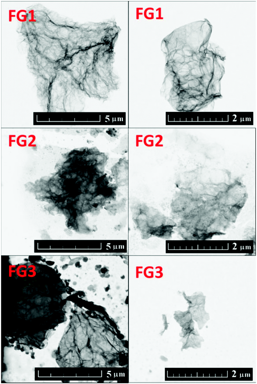 | ||
| Fig. 3 STEM images of fluorinated graphenes with various fluorine concentrations. | ||
The morphology was further investigated by atomic force microscopy (AFM). The images and the corresponding height profiles are shown in Fig. 4. All samples showed platelet structure with layer thickness ≤1 nm. A decreasing trend (down to 0.8 nm) in thickness with increasing the amount of fluorine was observed. The thickness of graphene monolayer is typically around 0.7–1.6 nm.31 The thickness of fluorographenes was determined to be around 0.6 nm by theoretical calculations.31 The measured data are in good agreement with those reported in the literature. These observations proved a successful synthesis of single layer fluorographene. The AFM images demonstrate that graphene sheets are etched not only on the sides, but some defects are also formed inside the layer planes. Most probably the etching starts at the places with highest energy such as defects and also on oxygen functionalities.
 | ||
| Fig. 4 AFM images of fluorinated graphenes with the corresponding height profiles. | ||
The formation of large defects and fragmentation of graphene sheets during the fluorination procedure are also documented by a significant increase of surface area measured by the BET method. For the first two samples a relatively small surface area is observed, 6.6 m2 g−1 and 5.4 m2 g−1 for FG1 and FG2, respectively. The full fluorination led to a significant increase of surface area to 320.4 m2 g−1. Such a large increase of surface area can be associated with defect formation and a reduction in size of large sheets.
The elemental composition was further measured using elemental combustion analysis (CHN-O). The results are summarized in Table 2. A systematic increase of fluorine concentration with increasing reaction time, pressure and temperature was observed. Simultaneously, the concentration of oxygen and hydrogen was lowered accordingly. This indicates that the remaining oxygen functional groups such as hydroxyls were substituted with fluorine. Similar results were obtained by EDS and XPS. The composition of the FG3 sample indicates a full fluorination and corresponds to white colour typical for wide band-gap materials like fluorographene – the fully fluorinated counterpart of graphene. Unusually a high concentration of nitrogen was also observed in FG3. This likely originated from the fluorine/nitrogen mixture used during the fluorination procedure. Reactive nitrogen compounds such as NF3 or NOF3 can be formed under reaction conditions and they can be introduced into the structure of fluorinated graphene.
| Sample | at% N | at% C | at% H | at% F | at% O |
|---|---|---|---|---|---|
| FG1 | 0.13 | 58.70 | 5.93 | 22.17 | 13.07 |
| FG2 | 0.11 | 41.68 | 0.55 | 42.62 | 15.04 |
| FG3 | 4.90 | 36.39 | 2.88 | 50.66 | 5.17 |
High resolution XPS was used to determine the chemical composition of fluorinated graphenes. The XPS survey spectra are presented in Fig. 5, where F 1s, C 1s and O 1s peaks are clearly visible. The F 1s peak was found at ∼687 eV, the C 1s peak at ∼284.5 eV and the O 1s peak at ∼533 eV. The composition of all fluorinated samples was calculated based on C 1s, O 1s and F 1s peak areas and the results are summarized in Table 3. Also the calculated C/F ratio is shown in Table 3. It can be clearly seen that the content of fluorine rises with more violent conditions. The C/F ratio varies between 0.95 and 2.72. The highest content of fluorine was found in FG3 and corresponds to the composition (C1F1.05)n. These results are in good agreement with the chemical analysis results discussed earlier.
 | ||
| Fig. 5 XPS survey spectra of fluorinated graphenes and deconvolution of the corresponding C 1s peaks. | ||
| at% | C/F | |||
|---|---|---|---|---|
| C | O | F | ||
| FG1 | 65.69 | 10.20 | 24.11 | 2.72 |
| FG2 | 53.00 | 9.24 | 37.76 | 1.40 |
| FG3 | 49.09 | 5.24 | 51.66 | 0.95 |
Further, detailed high resolution XPS spectra of the C 1s core level are shown in Fig. 5, while F 1s and O 1s details are presented in Fig. SI2.† The C 1s peaks with an asymmetrical tail at higher energies of fluorinated graphenes were fitted to quantitatively differentiate between nine different states of carbon bonding: C![[double bond, length as m-dash]](https://www.rsc.org/images/entities/char_e001.gif) C, C–C/C–H, C–O, CO, C–F, O–CO, π–π*, CF2 and CF3. The fitting was performed using energies 284.5 eV for CC; 285.5 eV for C–C/C–H; 286.7 eV for C–O; 288.2 eV for CO; 288.5 eV of C–F, 289.5 eV for O–CO; 290.8 eV for π–π* interaction; 291.0 eV for CF2 and 292.4 eV for CF3.32 The population of these bonds is summarized in Table SI1.† The highest amount of CF2 and CF3 bonds was found in FG3, which is in good agreement with all previously mentioned analyses.
C, C–C/C–H, C–O, CO, C–F, O–CO, π–π*, CF2 and CF3. The fitting was performed using energies 284.5 eV for CC; 285.5 eV for C–C/C–H; 286.7 eV for C–O; 288.2 eV for CO; 288.5 eV of C–F, 289.5 eV for O–CO; 290.8 eV for π–π* interaction; 291.0 eV for CF2 and 292.4 eV for CF3.32 The population of these bonds is summarized in Table SI1.† The highest amount of CF2 and CF3 bonds was found in FG3, which is in good agreement with all previously mentioned analyses.
FT-IR analysis in reflectance mode was used for the investigation of specific bond types in the prepared samples (Fig. 6). A wide band with a maximum ranging from 1000 to 1200 cm−1 can be seen in this figure. This band is characteristic for the C–F covalent bond. With increasing the amount of fluorine a shift of the C–F vibration band towards higher wavenumbers was observed. The band shifted from 1100 cm−1 for FG1 to 1135 cm−1 for FG2 and finally to 1200 cm−1 for FG3. Such a peak shift is related to a change of the C–F bond nature from “semi-ionic” to covalent type. The vibration band corresponding to CC bonds at 1590 cm−1 can be detected only in the FG1 sample with the lowest concentration of fluorine. The vibration band located at 1780 cm−1 and usually associated with CO vibration was observed only for the samples with lower fluorine content (FG1 and FG2).
 | ||
| Fig. 6 FT-IR spectra of fluorinated graphenes. | ||
In the next step, we performed the Raman spectroscopy using a 532 nm laser. Samples FG2 and FG3 exhibit very intense luminescence which led to the suppression of D and G band intensities. Since the exact values of intensity could not be obtained, the results of Raman spectroscopy are presented only graphically in Fig. 7. To reduce the problem with background luminescence the Raman spectroscopy was also performed using a UV laser with the wavelength of 325 nm (Fig. 7). The unusual shape of Raman spectra obtained using a UV laser has been reported previously and originates from different sensitivity towards sp2 and sp3 hybridized carbon atoms compared to excitation in the visible region of spectra.2 In Raman spectra two major peaks were detected. The first band, D-band, at 1430 cm−1, corresponds to sp3 hybridized carbon atoms and it is associated with defects in graphene structure and covalently bonded remaining oxygen functionalities. The second band, G-band, located at 1620 cm−1 corresponds to sp2 hybridized carbon atoms in graphene layers. The unusual shift towards higher wavenumber can be associated with covalently bonded fluorine to the graphene skeleton (usually the D-band is located at 1350 cm−1 and the G-band at 1580 cm−1).33 The D/G ratio obtained using a UV laser was 0.62 for FG1, 0.54 for FG2 and 0.43 for FG3. The Raman spectra of graphene used for fluorination are shown in the ESI (Fig. SI3†).
 | ||
| Fig. 7 Raman spectra of fluorinated graphenes recorded with a 325 nm laser (upper image) and a 532 nm laser (lower image). | ||
The structure of fluorinated graphenes was further investigated by X-ray diffraction (Fig. 8). The peak corresponding to the (001) reflection was found at 2θ = 14.4° for FG1, 2θ = 12.6° for FG2 and 2θ = 12.1° for FG3. This clearly indicates the increasing interlayer distance, which is typically 0.338 nm for pure graphite. Introduction of fluorine led to a significant increase of interlayer distance to 0.610 nm for FG1, 0.720 nm for FG2 and 0.731 nm for FG3.34 The increase of interlayer distance is associated with an increase of fluorine concentration. The broad diffraction peak associated with the (001) reflection also indicates a high degree of exfoliation. In addition the (101) reflection can be observed at 2θ = 44.46° and the (100) reflection at 2θ = 42.89°. In the case of the FG3 sample we can also observe a large broadening of the (101) and (100) reflection associated with the disorder induced by the fluorination procedure in fully fluorinated graphene.
 | ||
| Fig. 8 X-ray diffraction patterns of fluorinated graphenes. | ||
In the next step, thermal stability towards oxidation/combustion was tested using STA (Fig. 9) under a dynamic air atmosphere. The beginning of the oxidation started at 462 °C for FG1. Quite a surprising thermal behaviour was found for both the remaining highly-fluorinated samples FG2 and FG3. Higher content of fluorine led to a decrease in temperature of oxidation, which was 421 °C for FG2 and only 278 °C for FG3. All exothermal effects are accompanied by adequate weight losses. Let us note that an opposite trend was found for brominated graphenes and iodinated graphenes.19,20 This indicates that thermal stability of fluorinated graphene is closely related to not only the fluorine content, but also the degree of exfoliation and particle size. This is documented by BET surface area measurements where the sample FG3 has a significantly higher surface area compared to FG1 and FG2 samples.
 | ||
| Fig. 9 Thermal analysis of fluorinated graphenes. | ||
The photoluminescence spectroscopy confirms the assumptions of Raman spectra measurements, where a strong luminescence background significantly influenced the measurements (Fig. 10). While FG1 revealed only a weak luminescence, the luminescence of the FG3 sample was more than one order of magnitude higher. Undoubtedly, the increasing content of C–F bonds is responsible for higher photoluminescence. A blue shift of visible luminescence with increasing the fluorine concentration was observed. While the luminescence maximum of FG2 is located at 610 nm, it is shifted to 540 nm for the FG3 sample. The luminescence in the UV region was also detected; however, its intensity is significantly lower compared to the luminescence in the visible region (Fig. 10). Two maxima at 340 nm and 350 nm are clearly visible in the UV region. These wavelengths correspond to energies of 3.65 eV and 3.56 eV. This is rather close to the band-gap energy of 4.40 eV predicted theoretically for fluorographene.35 It is quite surprising that almost a similar spectrum in the UV region was observed for FG1 and FG2. This can be explained by the presence of highly fluorinated regions where electron–hole recombinations take place.
 | ||
| Fig. 10 The photoluminescence spectra of fluorinated graphene in the UV (left) and visible regions (right). | ||
In addition, the UV-VIS spectroscopy was performed on suspension in acetonitrile (Fig. SI4†). The highest absorbance, which is almost wavelength independent, was observed for the sample with lowest fluorine concentration (FG1). The absorbance of FG2 sample continuously increased to 320 nm, while in the FG3 sample a strong absorption starting at 320 nm and reaching the maximum at 270 nm was detected. This shows that fully fluorinated graphene can be used for surface coating with high transmittance in the NUV-VIS region.
The inherent electrochemistry was measured in the range of +0.5 V to −1.8 V. While the fully fluorinated graphene (FG3) showed none or only minimal reducible functional groups, both FG1 and FG2 revealed a clear reduction of the remaining oxygen functional groups starting at −0.3 V and reaching maxima at −0.95 V and −0.80 V for FG1 and FG2, respectively.36 The results of inherent electrochemistry measurements using 0.05 M PBS (pH = 7.0) as a supporting electrolyte are shown in the ESI (Fig. SI5†).
The heterogeneous electron transfer (HET) rate was measured using a [Fe(CN)6]3−/4− redox probe with 0.05 M PBS as a supporting electrolyte with pH = 7.0 (Fig. 12). The peak-to-peak separation was strongly dependent on the concentration of fluorine. The peak-to-peak (ΔEp–p) separation of FG1 and FG2 was 202 mV and 208 mV, while the fully fluorinated graphene FG3 exhibited a significantly larger (ΔEp–p) (369 mV) and thus slower HET which is comparable to the bare GC electrode (371 mV). Such a significant reduction of HET rate is related to low conductivity of fully fluorinated graphene.
In order to demonstrate the hydrophobic properties of fluorinated graphenes, we performed contact angle measurements on a silicon wafer coated with the tested material (Fig. 11). The results showed significant dependence of the contact angle on the fluorine concentration. The contact angle increased from 43.9° for FG1 to 86.8° for FG2 and finally to 142.2° for FG3. For comparison the contact angle measurement for the starting graphene is shown in the ESI (Fig. SI6†) documenting a substantially more hydrophilic behaviour with the contact angle of only 40.2°. Our results show that fully fluorinated graphene can be used for the preparation of super-hydrophobic surfaces.
 | ||
| Fig. 11 The contact angle of silicon wafer coated with fluorinated graphenes. | ||
 | ||
| Fig. 12 The HET rate of fluorinated graphenes using 0.01 M K4[Fe(CN)6] in 0.05 M PBS as a supporting electrolyte (pH = 7.0). | ||
Conclusions
Fluorinated graphenes were prepared by direct fluorination of thermally reduced graphenes obtained by microwave plasma assisted exfoliation of graphite oxide. The fluorine content in graphene was dependent on the reaction conditions. The developed method can be used for the synthesis of fluorinated graphene with a tunable concentration of fluorine up to fully fluorinated graphene – fluorographene with the overall composition of C1F1.05. Moreover the method can be easily scaled for mass production. Fluorographene can form a stable dispersion in non-aqueous solvent which is transparent in the NUV-VIS region. The synthesized materials were characterized in detail and etching of graphene during the fluorination procedure was analyzed by microscopic techniques. The studied materials exhibited a strong luminescence in the visible region of spectra whose maximum can be tuned by fluorine concentration. Fluorinated graphene can be applied for surface modification in order to prepare a surface coating with tunable hydrophobic properties. The fully fluorinated graphene can be used for the preparation of super-hydrophobic surfaces with great application potential.Acknowledgements
This project was supported by Czech Science Foundation (GACR no. 15-09001S) and by Specific University Research (MSMT no. 20/2015). Z. J. and F. Š. acknowledge support from the Institute of Organic Chemistry and Biochemistry, Academy of Science of the Czech Republic (Project no. RVO61388963).Notes and references
- A. K. Geim and K. S. Novoselov, Nat. Mater., 2007, 6, 183–191 CrossRef CAS PubMed.
- C. K. Chua, Z. Sofer, P. Šimek, O. Jankovský, K. Klímová, S. Bakardjieva, Š. Hrdličková Kučková and M. Pumera, ACS Nano, 2015, 9, 2548–2555 CrossRef CAS PubMed.
- L. Panchakarla, K. Subrahmanyam, S. Saha, A. Govindaraj, H. Krishnamurthy, U. Waghmare and C. Rao, Adv. Mater., 2009, 21, 4726–4730 CAS.
- L. Qu, Y. Liu, J.-B. Baek and L. Dai, ACS Nano, 2010, 4, 1321–1326 CrossRef CAS PubMed.
- C. Zhang, N. Mahmood, H. Yin, F. Liu and Y. Hou, Adv. Mater., 2013, 25, 4932–4937 CrossRef CAS PubMed.
- Z. Yang, Z. Yao, G. Li, G. Fang, H. Nie, Z. Liu, X. Zhou, X. a. Chen and S. Huang, ACS Nano, 2011, 6, 205–211 CrossRef CAS.
- O. Jankovský, P. Šimek, D. Sedmidubský, S. Matějková, Z. Janoušek, F. Šembera, M. Pumera and Z. Sofer, RSC Adv., 2013, 4, 1378–1387 RSC.
- R. R. Nair, W. Ren, R. Jalil, I. Riaz, V. G. Kravets, L. Britnell, P. Blake, F. Schedin, A. S. Mayorov and S. Yuan, Small, 2010, 6, 2877–2884 CrossRef CAS PubMed.
- O. Jankovský, P. Šimek, D. Sedmidubský, Š. Huber, M. Pumera and Z. Sofer, RSC Adv., 2014, 4, 7418–7424 RSC.
- O. Jankovský, P. Šimek, K. Klímová, D. Sedmidubský, M. Pumera and Z. Sofer, Carbon, 2015, 89, 121–129 CrossRef PubMed.
- Z. k. Sofer, O. e. Jankovský, P. Simek, K. i. Klímová, A. Macková and M. Pumera, ACS Nano, 2014, 8, 7106–7114 CrossRef CAS PubMed.
- M. Pumera, Chem. Soc. Rev., 2010, 39, 4146–4157 RSC.
- Z.-S. Wu, G. Zhou, L.-C. Yin, W. Ren, F. Li and H.-M. Cheng, Nano Energy, 2012, 1, 107–131 CrossRef CAS PubMed.
- L. Britnell, R. Gorbachev, R. Jalil, B. Belle, F. Schedin, A. Mishchenko, T. Georgiou, M. Katsnelson, L. Eaves and S. Morozov, Science, 2012, 335, 947–950 CrossRef CAS PubMed.
- M. S. Lavine, Science, 2014, 346, 1074–1074 Search PubMed.
- J. O. Sofo, A. S. Chaudhari and G. D. Barber, Phys. Rev. B: Condens. Matter, 2007, 75, 153401 CrossRef.
- K.-J. Jeon, Z. Lee, E. Pollak, L. Moreschini, A. Bostwick, C.-M. Park, R. Mendelsberg, V. Radmilovic, R. Kostecki, T. J. Richardson and E. Rotenberg, ACS Nano, 2011, 5, 1042–1046 CrossRef CAS PubMed.
- D. K. Samarakoon, Z. Chen, C. Nicolas and X. Q. Wang, Small, 2011, 7, 965–969 CrossRef CAS PubMed.
- P. Šimek, K. Klímová, D. Sedmidubský, O. Jankovský, M. Pumera and Z. Sofer, Nanoscale, 2015, 7, 261–270 RSC.
- O. Jankovský, P. Šimek, K. Klimová, D. Sedmidubský, S. Matějková, M. Pumera and Z. Sofer, Nanoscale, 2014, 6, 6065–6074 RSC.
- F. Withers, M. Dubois and A. K. Savchenko, Phys. Rev. B: Condens. Matter, 2010, 82, 073403 CrossRef.
- M. Chen, C. Qiu, H. Zhou, H. Yang, F. Yu and L. Sun, J. Nanosci. Nanotechnol., 2013, 13, 1331–1334 CrossRef CAS PubMed.
- T. Nakajima, V. Gupta, Y. Ohzawa, H. Groult, Z. Mazej and B. Žemva, J. Power Sources, 2004, 137, 80–87 CrossRef CAS PubMed.
- A. Y. S. Eng, Z. Sofer, P. Šimek, J. Kosina and M. Pumera, Chem. – Eur. J., 2013, 19, 15583–15592 CrossRef CAS PubMed.
- U. Hofmann and A. Frenzel, Kolloidn. Zh., 1934, 68, 149–151 CAS.
- C. H. A. Wong, O. Jankovský, Z. Sofer and M. Pumera, Carbon, 2014, 77, 508–517 CrossRef CAS PubMed.
- M. Valasek, F. Sembera, M. J. Hughes, I. Stibor, Z. Janousek and J. Michl, in Efficient Preparations of Fluorine Compounds, ed. H. W. Roesky, John Wiley & Sons, Inc., 2012, pp. 22–25 Search PubMed.
- R. S. Nicholson, Anal. Chem., 1965, 37, 1351–1355 CrossRef CAS.
- S. J. Konopka and B. McDuffie, Anal. Chem., 1970, 42, 1741–1746 CrossRef CAS.
- N. A. Nebogatikova, I. V. Antonova, V. Y. Prinz, I. I. Kurkina, V. I. Vdovin, G. N. Aleksandrov, V. B. Timofeev, S. A. Smagulova, E. R. Zakirov and V. G. Kesler, Phys. Chem. Chem. Phys., 2015, 17, 13257–13266 RSC.
- L. Pu, Y. Ma, W. Zhang, H. Hu, Y. Zhou, Q. Wang and C. Pei, RSC Adv., 2013, 3, 3881–3884 RSC.
- X. Wang, Y. Dai, J. Gao, J. Huang, B. Li, C. Fan, J. Yang and X. Liu, ACS Appl. Mater. Interfaces, 2013, 5, 8294–8299 CAS.
- O. Jankovsky, S. Hrdlickova Kuckova, M. Pumera, P. Simek, D. Sedmidubsky and Z. Sofer, New J. Chem., 2014, 38, 5700–5705 RSC.
- Z. Sofer, P. Simek, O. Jankovsky, D. Sedmidubsky, P. Beran and M. Pumera, Nanoscale, 2014, 6, 13082–13089 RSC.
- F. Karlický and M. Otyepka, J. Chem. Theory Comput., 2013, 9, 4155–4164 CrossRef.
- E. L. K. Chng and M. Pumera, Chem. – Asian J., 2011, 6, 2899–2901 CrossRef CAS PubMed.
Footnote |
| † Electronic supplementary information (ESI) available. See DOI: 10.1039/c5nr03243a |
| This journal is © The Royal Society of Chemistry 2015 |