
 Open Access Article
 This Open Access Article is licensed under a
 Creative Commons Attribution 3.0 Unported Licence
Nanostructured cavity devices for extracellular stimulation of HL-1 cells†
Anna
Czeschik
a,
Philipp
Rinklin
a,
Ulrike
Derra
a,
Sabrina
Ullmann
a,
Peter
Holik
b,
Siegfried
Steltenkamp
b,
Andreas
Offenhäusser
 ac and
Bernhard
Wolfrum
*ac
ac and
Bernhard
Wolfrum
*ac
aInstitute of Bioelectronics (PGI-8/ICS-8), Forschungszentrum Jülich and JARA – Fundamentals of Future Information Technologies, 52425 Jülich, Germany. E-mail: b.wolfrum@fz-juelich.de
bMicro Systems Technology (MST), Center of Advanced European Studies and Research (caesar), 53175 Bonn, Germany
cIV. Institute of Physics, RWTH Aachen University, 52074 Aachen, Germany
First published on 24th April 2015
Abstract
Microelectrode arrays (MEAs) are state-of-the-art devices for extracellular recording and stimulation on biological tissue. Furthermore, they are a relevant tool for the development of biomedical applications like retina, cochlear and motor prostheses, cardiac pacemakers and drug screening. Hence, research on functional cell-sensor interfaces, as well as the development of new surface structures and modifications for improved electrode characteristics, is a vivid and well established field. However, combining single-cell resolution with sufficient signal coupling remains challenging due to poor cell-electrode sealing. Furthermore, electrodes with diameters below 20 µm often suffer from a high electrical impedance affecting the noise during voltage recordings. In this study, we report on a nanocavity sensor array for voltage-controlled stimulation and extracellular action potential recordings on cellular networks. Nanocavity devices combine the advantages of low-impedance electrodes with small cell-chip interfaces, preserving a high spatial resolution for recording and stimulation. A reservoir between opening aperture and electrode is provided, allowing the cell to access the structure for a tight cell-sensor sealing. We present the well-controlled fabrication process and the effect of cavity formation and electrode patterning on the sensor's impedance. Further, we demonstrate reliable voltage-controlled stimulation using nanostructured cavity devices by capturing the pacemaker of an HL-1 cell network.
Introduction
Merging biological tissue and electronics provides versatile opportunities for research in biomedical and life sciences. On-chip technologies are used for pharmacological studies and drug screening,1,2 retina and cochlear investigations,3,4 amperometric neurotransmitter detection5,6 and voltammetric applications like action potential recordings and stimulation of single cells and networks.7–11 Electrode impedance, sealing resistance between cell and sensor, electrode size, and density are the most important parameters for on-chip electrophysiology since they correlate with the signal-to-noise ratio and spatial resolution.12 A high electrode density is given by microelectrode arrays (MEAs), which are the tools of choice in many extracellular in vitro and in vivo investigations.13 The use of MEAs facilitates non-invasive, highly parallelized electrophysiological recordings14,15 and neuroelectrochemical measurements.16,17 Hence, they provide an interesting alternative to probe-based techniques that are currently the gold standard for this type of measurements. For instance, MEAs can be used for the detection of neurotransmitter release on the network level as opposed to carbon fiber electrodes.6,18 In general, cells can be cultured on chip-based sensors up to several weeks or months enabling long-term experiments. MEAs are fabricated with arbitrary electrode sizes on silicon- or glass-based substrates with CMOS or CMOS-independent processes.11,19,20 The optimal electrode size for a certain application is usually selected by weighing spatial resolution and the performance of stimulation and recording capabilities as the determining factors. While small electrode sizes (typically below 100 µm2) are beneficial for low-noise amperometric recordings, dense electrode packaging, and full coverage by the cell, bigger electrodes provide a larger cell-electrode interface and better noise characteristics for voltage recordings.Optimizing the physical interface properties remains a major task in bioelectronics.12,21 Various attempts in material research and design of sensor surfaces aim for a functional cell-sensor interface and an efficient signal transmission. Different layouts have been realized to support cell guidance,22 adherence,21 and sealing23 for electrical and chemical recording. Approaches for improving the cell-sensor interface include: surface modifications by nanopores, -pillars,24,25 -spines26,27 and -wires,28,29 as well as neurocages,30 graphene31 and carbon nanotubes32–35 or interdigitated geometries.36 For voltage recordings, low-impedance electrodes support a high signal-to-noise ratio. At the same time, a low impedance improves the charge transfer capabilities for cell stimulation. Furthermore, a high sealing resistance is required for obtaining low leakage currents and a strong signal transfer.37 The electrode impedance is determined by the sensor's interface capacitance as well as possible faradaic contributions. Therefore, a large electrode-electrolyte interface lowers the electrode impedance and is hence favorable for signal transduction. Nanocavity arrays have been presented as a method to efficiently combine the need for a large electrode area with a high spatial resolution.38–40 This sensor type consists of a well-defined cavity between electrode and passivation layer and a small opening aperture that connects the cavity to the cell. Consequently, similar to the planar patch clamp method,41,42 a low sensor impedance is combined with a high spatial resolution at the single-cell level. The advantage of the nanocavity approach lies in the possibility to integrate many devices at a high density to record from or stimulate multiple cells within a single network.
Previously, we have presented planar nanocavity sensors based on sacrificial layer etching, which exhibited low electrical impedance combined with good recording capabilities of action potentials.38,40
In this study, we introduce a new cavity device with a nanostructured electrode interface. We investigate electrical impedance and cell-sensor coupling for stimulation applications. To this end, we demonstrate voltage-controlled stimulation of HL-1 cells using nanocavity arrays and analyze the modulated pacing of a cardiac network.
Methods
Device fabrication
The fabrication of nanocavity sensors was adapted from previously described methods.38,40 Microelectrode arrays were produced by standard optical lithography in a cleanroom environment (ISO 4). 64 Ti/Au/Cr feedlines were fabricated using optical lithography and passivated by PECVD, with a stack of alternating SiO2 and Si3N4 layers at 300 °C. The electrodes were opened by reactive ion etching. Chromium etch solution (Chrome Etch No. 1, MicroChemicals) containing ceric ammonium nitrate and perchloric acid was used to generate nanocavites with adjustable length.Cell culture
The cardiomyocyte-like cell line HL-1 was cultured in Claycomb medium with 10% FBS, 100 µg ml−1 penicillin-streptomycin, 0.1 mM norepinephrine and 2 mM L-glutamine in a humidified atmosphere at 37 °C and 5% CO2. The cells were split after reaching confluency two times per week by applying 0.05% Trypsin/EDTA.43 After splitting, cells were plated on fibronectin/gelatin coated chips and grown until confluency was reached.Impedance spectroscopy
Impedance measurements were performed during the etching process at four electrodes simultaneously, using a multichannel potentiostat (VSP300, Biologic), an Ag/AgCl quasi-reference electrode, and a gold wire as counter electrode. 17 measurement loops were performed in a frequency range of 1 Hz–10 kHz with a voltage amplitude of 0.2 V versus Ag/AgCl. The waiting time between every loop was set to 10 s. The overall measurement time was around 800 s.Calcium imaging and extracellular electrophysiology
For optical control of electrical activity, HL-1 samples were stained with a calcium-sensitive dye (Fluo-4, AM). While performing recording or stimulating experiments, calcium fluorescence signals were observed via a high speed, low light EMCCD camera (Hamamatsu C9100-13). Action potential recordings were acquired with a custom-made combination of a 64-channel amplifier and pre-amplifier headstage, which provide an overall gain of 1000. Cells growing on the nanocavity arrays were stimulated with trains of biphasic square pulses with a voltage amplitude of 0.9 V and a frequency of 250 Hz. For the experiments, an Ag/AgCl quasi-reference electrode was used.FIB sample preparation
Cells on chips were washed two times with pre-warmed PBS and fixed with a solution of 3% glutaraldehyde in PBS for 20 min at room temperature. Afterwards, glutaraldehyde was removed and samples were washed with PBS four times, before dehydration by placing the samples for 5 min at a time in a concentration cascade of ethanol (10%–100%). Samples were prepared for imaging by critical point drying and sputtered with iridium before being inserted in a Helios Nanolab Dualbeam (FEI, Hillsboro, USA) FIB/SEM system.Results and discussion
Nanocavity MEAs for on-chip electrophysiology were fabricated using standard clean room technology (see Experimental section). Gold microelectrode arrays with an electrode opening of 12 or 24 µm were chosen for the fabrication of nanocavity sensors for voltammetric applications. After cleanroom fabrication of the MEAs, the chromium adhesion layer (thickness in the range of 100 nm) was chemically removed along the feedlines by chromium etch solution. The microscopic control of this process revealed an etching of approx. 48 µm in 5 min to produce cavities between the metal layer and the SiO2/Si3N4 passivation (Fig. 1a). Images showing the progression of the etching front at different time stamps are shown in the inset of the figure. The formation of nanocavities is a well-controlled process, which can be tuned to the desired length of the nanocavity by exchanging the etching solution with water at an appropriate time. For long time-scales, the etching progress of the chromium sacrificial layer approaches a square-root dependence of time (x ∼ sqrt(t)) as expected for a diffusion limited process. The electrode impedance is inversely proportional to the electrode area. Thus, a large electrode/electrolyte interface is highly beneficial for on-chip electrophysiology and – combined with a high junction resistance between cell and sensor – of paramount importance for a good signal-to-noise ratio. We evaluated the effect of cavity etching on the impedance of the device by performing impedance spectroscopy during the etching process. In Fig. 1b, the absolute impedance values are shown in dependence of the etching time. At the end of an 800 s etching process, a decrease in impedance of about one order of magnitude can be observed. At the beginning of the etching process, when the cavity formation is initiated, the impedance is in the order of 4.3 × 10⁶ Ω and 6 × 10⁵ Ω for 1 kHz and 10 kHz, respectively. The specific capacitance lies in the range of 27 µF cm−2. From the microscopic time lapse images in Fig. 1a, we can see the progression of the cavity etching over time. During the etching process, a continuous decrease in impedance is observed until the cavity length reaches approx. 80 µm (corresponding to ∼600 s etching time) (Fig. 1b). At this point, effects of a larger electrode-electrolyte interface are masked by the ohmic resistance of the narrow cavity. Hence, the limiting factor for impedance improvement for long cavities is the ohmic drop inside the nanochannel. The back-etched electrodes show a relatively high specific capacitance in the range of 300 µF cm−2. This is approximately one order of magnitude higher than the usually observed value for planar gold surfaces.44 An increased specific electrode capacitance is generally caused by a high surface roughness of the interface. In fact, several approaches aim at increasing the capacitance of the electrodes by introducing nanopatterned interfaces. Here, we ascribe this effect to interdiffusion phenomena at the Au/Cr interface, caused by the high temperatures used in our fabrication process (300 °C). | ||
| Fig. 1 Nanocavity length, measured from the aperture's edge in feedline direction, over etching time (a). This well-controlled process allows for an easy tuning of the nanocavity length. Inset: etching progress at different time stamps. The etch front, progressing from right to left along the feed line, is indicated by the sharp transition from white to grey. Impedance data (mean ± standard deviation, (N = 4)) as a function of etching time for probing frequencies of 1 kHz and 10 kHz at different points during the etching process (b). The impedance decreases with increasing etching time until at 600 s (∼80 µm cavity size) the ohmic resistance of the narrow cavity starts to mask the effect of a larger electrode-electrolyte interface. | ||
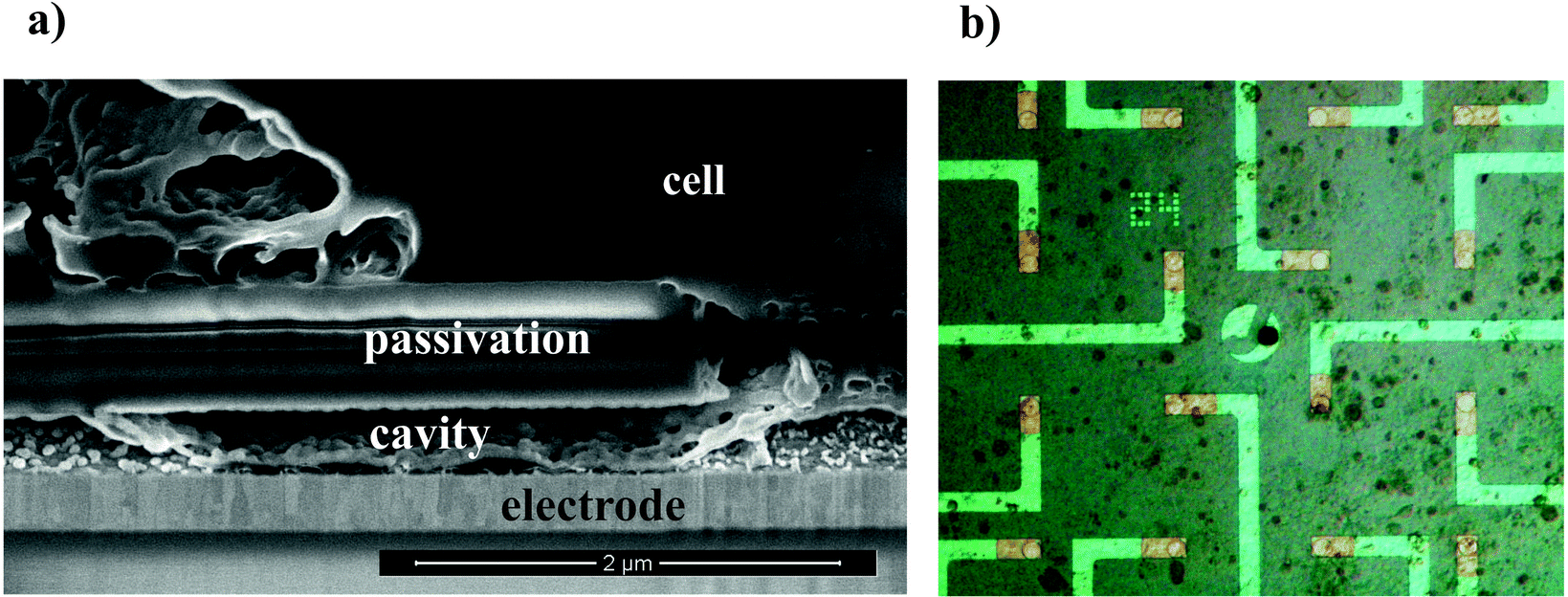
Paired with the subsequent removal of the chromium, this process introduces a rough gold surface,45,46 which can be observed by scanning electron microscopy (SEM) at the cavity-electrode interface (Fig. 2a). Apart from affecting the electrical properties of the interface, a rough electrode surface can be advantageous with regard to cell coupling as it supports cell and protein adhesion.47,48 A crucial factor, which influences the sensing and stimulation performance of a functional device, is the cell-substrate interface. A low resistance of this junction alters signal transmission between cell membrane and sensor and reduces the signal transfer significantly. It has been shown that the seal resistance for nanocavity devices can lie in the range of several tens of MΩs, an order of magnitude higher compared to standard plain MEAs.39 Here, we evaluated the cell-sensor-interface by SEM in combination with focused ion beam (FIB) sectioning, as shown in Fig. 2a. The cell tightly covers the sensor, while the cleft between cell and electrode is small. Remarkably, parts of the cell seem to grow inside the channel covering the nanostructured electrode. The ability of cells to penetrate into microstructures49 is well known and utilized in applications like spatial separation,50 cell trapping30 or guided growth.51 Here, we demonstrate that HL-1 cells are also capable of penetrating much smaller channel-like structures, which exhibit a height of only around 180 nm, providing a tight cell-device sealing.
 | ||
| Fig. 2 Focused ion beam (FIB) cross section of an HL-1 cell on a nanocavity sensor (a). In-between passivation and electrode, cellular protrusion into the cavity can be observed. The cleft between cell and electrode is small, allowing for a tight sensor-cell sealing and therefore a good signal transduction. Nanocavity chip with electrode openings of 24 µm (b). HL-1 cells have been cultured on chip for several days. Back-etched cavities can be seen as rectangular structures along the feedlines. | ||
The stability of the devices under cell culture conditions was tested by culturing cardiomyocyte-like cells (HL-1) on the chip for several days (see Fig. 2b). We evaluated the electrical functionality of the arrays by recording action potentials from HL-1 cells at multiple channels simultaneously. When confluent, HL-1 cells start contracting and firing action potentials spontaneously. Therefore, they represent an optimal model system for electrophysiological measurements. Fig. 3 displays exemplary voltage traces of 3 channels showing action potential recordings from HL-1 cells. To remove artifacts, which originate from the camera trigger, AP recordings have been smoothed by a Savitzky–Golay filter (window size of 51, 3rd order polynomial, unfiltered data shown in Fig. S1, see ESI†). The action potentials have a peak-to-peak amplitude in the range of 1 mV and a signal-to-noise ratio of about 50 (peak-to-peak signal versus peak-to-peak noise). The propagation of the electrical signals through the cell layer and the spatial resolution of the device are illustrated by the temporal difference of signals recorded with channels, located at different positions on the chip. Calculated from the three exemplary traces, the propagation velocity of the action potential wave is approx. 11 mm s−1.
 | ||
| Fig. 3 Action potential recordings performed with nanocavity arrays. Shown are three channels, the traces are smoothed by a Savitzky–Golay-filter. The beating behavior over a time span of ∼30 s is shown in (a). (b) Shows single beating events of the same traces at a higher time resolution. The temporal shift of the three spikes becomes evident indicating the propagation of the action potential across the cell layer. | ||
In this study, we focused on the evaluation of localized voltage-controlled stimulation using nanocavity devices. To evaluate the cell activity independent of electrical measurements, we performed simultaneous optical recordings. By using a calcium-sensitive fluorescent dye (Fluo-4, AM) it is possible to visualize intracellular calcium concentrations correlated with the occurrence of action potentials.52 The graph in Fig. S2 (see ESI†) shows electrical signals captured from five channels (blue) and the correlated optical fluorescence signal, extracted from areas of interest above the corresponding electrodes (red overlay). Although the calcium signal is significantly slower than the electrical action potentials, the correlation is clearly visible. The staining of the confluent cell layer on the chip leads to the observation of a fluorescent propagating calcium wave through the confluent cell layer. This can be utilized for the optical evaluation of stimulation experiments52 without electrical recordings, which are often distorted during the stimulation process via crosstalk.53
For the stimulation experiments, we applied biphasic square wave pulses with a duty cycle of 30, a frequency of 250 Hz and amplitudes between 600 mV and 900 mV. 30 pulses were repeated within a 60 s time frame generating a stimulation pattern of approximately 0.5 Hz. The calcium fluorescence intensities at the 16 electrodes within the sample image were extracted and plotted over time (Fig. 4). The upper graph shows a rather irregular behavior of the unstimulated HL-1 layer (Fig. 4a). The lower graph displays the cell network's response to the stimulation in terms of a higher beating frequency and an increased regularity (Fig. 4b). The data unequivocally shows that the signal, which is applied via the nanocavities, forces the beating pattern of the HL-1 network to fall in line with the stimulation frequency. This circumstance gets even more explicit by calculating the mean spike frequencies for the stimulated and unstimulated network as shown in Fig. 5. We see that the beating pattern of the stimulated network is increased to the stimulation frequency. At the same time, the variations in the beating pattern (standard deviation) is significantly reduced, highlighting the reliability of the stimulation process.
 | ||
| Fig. 4 Calcium fluorescence signals from 16 regions of interests without (a) and with (b) stimulation. The spontaneous beating activity (no stimulation, a) is rather irregular. When applying voltage pulses, the optical signal follows the regular stimulation pattern (b). The signal applied via the nanocavities thus clearly forces the beating pattern of the HL-1 network to fall in line with the stimulation frequency. | ||
 | ||
| Fig. 5 Mean spike frequencies, calculated on basis of the cross-correlation analysis of calcium imaging videos. In the stimulated case, the frequency is increased to the stimulation frequency while the variation in the beating pattern is significantly reduced as compared to the spontaneous activity. | ||
To further analyze the network response to prolonged stimulation, calcium imaging videos of spontaneous as well as stimulated beating activity were recorded and subsequently analyzed by a Matlab script to perform a cross-correlation analysis of the local fluorescence intensity. The propagation plots can be seen in Fig. 6. In this experiment, one minute videos with alternating applied and non-applied stimulation protocols were recorded and used for data analysis. While the spontaneous calcium wave starts at the bottom of the image and propagates to the top, the onset of four electrode stimulation in the center of the sample triggers the calcium wave to originate in the center before propagating to the outer periphery. This “high-jacking” effect on the cells pacemaker can be repeated several times. In Fig. 6 a cycle of three stimulation onsets is shown. After each stimulation period, the cells return to their intrinsic beating behavior. This influence on the signal conduction could be used in future applications for investigation of cardiac arrhythmia by creating activity pattern connected to fibrillation. After the second stimulation period (Fig. 6d) a shift of the wave front to a more horizontal orientation was observed (Fig. 6e). Similar effects have been observed during cardiac conduction blocking with high-frequency signals as shown in the work of Dura et al.54 Also it has been reported, that rapid stimulation can cause electrical remodeling of cardiac cells, which might lead to increased vulnerability to atrial fibrillation.55 We assume that the change in action potential direction is a pre-stage to stimulation induced occurrence of fibrillation phenomena on a cellular level.56
 | ||
| Fig. 6 Cross-correlation analysis of calcium imaging videos. The time delay of the propagating action potential front is color coded, referring to the color scale in (a) x- and y-axis give the dimensions of the observed sample section. A voltage-controlled stimulation protocol has been applied in every second measurement (b, d, f) to high-jack the cell's pacemaker and change the network's beating behavior. Spontaneous activity can be seen in (a), (c) and (e). Every image represents the same position on the same sample. | ||
Conclusions
The presented approach for MEA modification by introducing nanocavities is a simple, easily realizable and well controlled way to improve electrode characteristics. The process significantly lowers the electrode impedance and promotes cell-sensor sealing by allowing cells to protrude into the cavity. This represents a novel concept for directed growth into the nanostructure, which could be utilized for cell guidance. Nanocavity arrays show great potential for on chip electrophysiology, as was demonstrated by action potential recordings and voltage-controlled stimulation experiments on cardiomyocyte-like HL-1 cells at multiple channels simultaneously. The presented device further provides possibilities for investigation of intercellular communication as well as cardiac phenomena like stimulation-induced arrhythmia and pacing. We see future applications in the combination of nanocavity devices and guided cell growth. Guided neurites growing into a functionalized cavity could improve cell-chip coupling for localized neurotransmitter recording and investigations on cellular communication.Acknowledgements
We thank Marko Banzet for clean-room processing and Francesca Santoro and Elke Brauweiler-Reuters for help with FIB-sample preparation and FIB cuts. Additionally, we thank Norbert Wolters for building the amplifier system and Dieter Lomparski and Fabian Brings for software development and support in signal analysis. We gratefully acknowledge funding by the Helmholtz Young Investigators program.Notes and references
- H.-F. Cui, J.-S. Ye, Y. Chen, S.-C. Chong and F.-S. Sheu, Anal. Chem., 2006, 78, 6347–6355 CrossRef CAS PubMed.
- G. Xiang, L. Pan, L. Huang, Z. Yu, X. Song, J. Cheng, W. Xing and Y. Zhou, Biosens. Bioelectron., 2007, 22, 2478–2484 CrossRef CAS PubMed.
- A. E. Grumet, J. L. Wyatt and J. F. Rizzo, J. Neurosci. Methods, 2000, 101, 31–42 CrossRef CAS.
- M. S. Humayun, E. de Juan, J. D. Weiland, G. Dagnelie, S. Katona, R. Greenberg and S. Suzuki, Vision Res., 1999, 39, 2569–2576 CrossRef CAS.
- I. Hafez, K. Kisler, K. Berberian, G. Dernick, V. Valero, M. G. Yong, H. G. Craighead and M. Lindau, Proc. Natl. Acad. Sci. U. S. A., 2005, 102, 13879–13884 CrossRef CAS PubMed.
- A. Yakushenko, E. Kätelhön and B. Wolfrum, Anal. Chem., 2013, 85, 5483–5490 CrossRef CAS PubMed.
- J. Pine, J. Neurosci. Methods, 1980, 2, 19–31 CrossRef CAS.
- L. Berdondini, P. D. van der Wal, O. Guenat, N. F. de Rooij, M. Koudelka-Hep, P. Seitz, R. Kaufmann, P. Metzler, N. Blanc and S. Rohr, Biosens. Bioelectron., 2005, 21, 167–174 CrossRef CAS PubMed.
- G. T. Kovacs, C. W. Storment and J. M. Rosen, IEEE Trans. Biomed. Eng., 1992, 39, 893–902 CrossRef CAS PubMed.
- C. A. Thomas, P. A. Springer, G. E. Loeb, Y. Berwald-Netter and L. M. Okun, Exp. Cell Res., 1972, 74, 61–66 CrossRef.
- W. L. C. Rutten, Annu. Rev. Biomed. Eng., 2002, 4, 407–452 CrossRef CAS PubMed.
- A. Blau, C. Ziegler, M. Heyer, F. Endres, G. Schwitzgebel, T. Matthies, T. Stieglitz, J. U. Meyer and W. Göpel, Biosens. Bioelectron., 1997, 12, 883–892 CrossRef CAS.
- A. Stett, U. Egert, E. Guenther, F. Hofmann, T. Meyer, W. Nisch and H. Haemmerle, Anal. Bioanal. Chem., 2003, 377, 486–495 CrossRef CAS PubMed.
- S. Stoelzle, A. Obergrussberger, A. Brüggemann, C. Haarmann, M. George, R. Kettenhofen and N. Fertig, Front. Pharmacol., 2011, 2, 76 CAS.
- O. P. Hamill, A. Marty, E. Neher, B. Sakmann and F. J. Sigworth, Pfluegers Arch., 1981, 391, 85–100 CrossRef CAS.
- R. H. Chow, L. von Rüden and E. Neher, Nature, 1992, 356, 60–63 CrossRef CAS PubMed.
- L. J. Breckenridge, R. J. Wilson, P. Connolly, A. S. G. Curtis, J. A. T. Dow, S. E. Blackshaw and C. D. Wilkinson, J. Neurosci. Res., 1995, 42, 266–276 CrossRef CAS PubMed.
- J. Wang, R. Trouillon, Y. Lin, M. I. Svensson and A. G. Ewing, Anal. Chem., 2013, 85, 5600–5608 CrossRef CAS PubMed.
- A. Hierlemann, U. Frey, S. Hafizovic and F. Heer, Proc. IEEE, 2011, 99, 252–284 CrossRef CAS.
- F. Heer, W. Franks, A. Blau, S. Taschini, C. Ziegler, A. Hierlemann and H. Baltes, Biosens. Bioelectron., 2004, 20, 358–366 CrossRef CAS PubMed.
- A. Blau, Curr. Opin. Colloid Interface Sci., 2013, 18, 481–492 CrossRef CAS PubMed.
- L. Griscom, P. Degenaar, B. Lepiou, E. Tamiya and H. Fujita, Sens. Actuators, 2002, 83, 15–21 CrossRef CAS.
- M. E. Spira and A. Hai, Nat. Nanotechnol., 2013, 8, 83–94 CrossRef CAS PubMed.
- M. Wesche, M. Hüske, A. Yakushenko, D. Brüggemann, D. Mayer, A. Offenhäusser and B. Wolfrum, Nanotechnology, 2012, 23, 495303 CrossRef PubMed.
- D. Brüggemann, B. Wolfrum, V. Maybeck, Y. Mourzina, M. Jansen and A. Offenhäusser, Nanotechnology, 2011, 22, 265104 CrossRef PubMed.
- A. Hai, J. Shappir and M. E. Spira, Nat. Methods, 2010, 7, 200–202 CrossRef CAS PubMed.
- F. Santoro, J. Schnitker, G. Panaitov and A. Offenhäusser, Nano Lett., 2013, 13, 5379–5384 CrossRef CAS PubMed.
- T. Cohen-Karni, B. P. Timko, L. E. Weiss and C. M. Lieber, Proc. Natl. Acad. Sci. U. S. A., 2009, 106, 7309–7313 CrossRef CAS PubMed.
- R. A. Beckman, E. Johnston-Halperin, N. A. Melosh, Y. Luo, J. E. Green and J. R. Heath, J. Appl. Phys., 2004, 96, 5921 CrossRef CAS PubMed.
- E. Meng and J. O. N. Erickson, IEEE Eng. Med. Biol. Mag., 2005, 30–33 Search PubMed.
- M. Dankerl, M. V. Hauf, A. Lippert, L. H. Hess, S. Birner, I. D. Sharp, A. Mahmood, P. Mallet, J.-Y. Veuillen, M. Stutzmann and J. A. Garrido, Adv. Funct. Mater., 2010, 20, 3117–3124 CrossRef CAS PubMed.
- K. Wang, H. A. Fishman, H. Dai and J. S. Harris, Nano Lett., 2006, 6, 2043–2048 CrossRef CAS PubMed.
- X. Luo, C. L. Weaver, D. D. Zhou, R. Greenberg and X. T. Cui, Biomaterials, 2011, 32, 5551–5557 CrossRef CAS PubMed.
- L. Bareket-Keren and Y. Hanein, Front. Neural Circuits, 2012, 6, 122 Search PubMed.
- M. David-Pur, L. Bareket-Keren, G. Beit-Yaakov, D. Raz-Prag and Y. Hanein, Biomed. Microdevices, 2014, 16, 43–53 CrossRef CAS PubMed.
- M.-C. Chuang, H.-Y. Lai, J.-A. Annie Ho and Y.-Y. Chen, Biosens. Bioelectron., 2013, 41, 602–607 CrossRef CAS PubMed.
- W. L. C. Rutten, Annu. Rev. Biomed. Eng., 2002, 4, 407–452 CrossRef CAS PubMed.
- B. Hofmann, E. Kätelhön, M. Schottdorf, A. Offenhäusser and B. Wolfrum, Lab Chip, 2011, 11, 1054–1058 RSC.
- M. Schottdorf, B. Hofmann, E. Kätelhön, A. Offenhäusser and B. Wolfrum, Phys. Rev. E: Stat. Phys., Plasmas, Fluids, Relat. Interdiscip. Top., 2012, 85, 031917 CrossRef.
- A. Czeschik, A. Offenhäusser and B. Wolfrum, Phys. Status Solidi, 2014, 211, 1462–1466 CrossRef CAS PubMed.
- N. Fertig, R. H. Blick and J. C. Behrends, Biophys. J., 2002, 82, 3056–3062 CrossRef CAS.
- X. Li, K. G. Klemic, M. A. Reed and F. J. Sigworth, Nano Lett., 2006, 6(4), 815–819 CrossRef CAS PubMed.
- W. C. Claycomb, N. A. Lanson, B. S. Stallworth, D. B. Egeland, J. B. Delcarpio, A. Bahinski and N. J. Izzo, Proc. Natl. Acad. Sci. U. S. A., 1998, 95, 2979–2984 CrossRef CAS.
- S. E. Moulton, J. N. Barisci, A. Bath, R. Stella and G. G. Wallace, Electrochim. Acta, 2004, 49, 4223–4230 CrossRef CAS PubMed.
- G. Majni, G. Ottaviani and M. Prudenziati, Thin Solid Films, 1976, 38, 15–19 CrossRef CAS.
- R. A. Sigsbee, Metall. Trans., 1971, 2, 719–722 CrossRef.
- A. F. von Recum, C. E. Shannon, C. E. Cannon, K. J. Long, T. G. van Kooten and J. Meyle, Tissue Eng., 1996, 2, 241–253 CrossRef PubMed.
- N. J. Hallab, K. J. Bundy, K. O'Connor, R. L. Moses and J. J. Jacobs, Tissue Eng., 2001, 7, 55–71 CrossRef CAS PubMed.
- J.-M. Peyrin, B. Deleglise, L. Saias, M. Vignes, P. Gougis, S. Magnifico, S. Betuing, M. Pietri, J. Caboche, P. Vanhoutte, J.-L. Viovy and B. Brugg, Lab Chip, 2011, 11, 3663–3673 RSC.
- A. Leclerc, D. Tremblay, S. Hadjiantoniou, N. V. Bukoreshtliev, J. L. Rogowski, M. Godin and A. E. Pelling, Biomaterials, 2013, 34, 8097–8104 CrossRef CAS PubMed.
- M. J. Mahoney, R. R. Chen, J. Tan and W. M. Saltzman, Biomaterials, 2005, 26, 771–778 CrossRef CAS PubMed.
- N. Herzog, M. Shein-Idelson and Y. Hanein, J. Neural Eng., 2011, 8, 056008 CrossRef PubMed.
- R. H. Olsson, D. L. Buhl, A. M. Sirota, G. Buzsaki and K. D. Wise, IEEE Trans. Biomed. Eng., 2005, 52, 1303–1311 CrossRef PubMed.
- B. Dura, G. T. A. Kovacs and L. Giovangrandi, PLoS One, 2012, 7, e36217 CAS.
- Z. Yang, W. Shen, J. N. Rottman, J. P. Wikswo and K. T. Murray, J. Mol. Cell. Cardiol., 2005, 38, 299–308 CrossRef CAS PubMed.
- S. Jacquir, S. Binczak, D. Vandroux, G. Laurent, P. Athias and J. M. Bilbault, Comput. Cardiol., 2008, 625–628 Search PubMed.
Footnote |
| † Electronic supplementary information (ESI) available: Comparison of non-filtered and Savitzky–Golay filtered action potential recordings, electrical signals and corresponding optical signals. See DOI: 10.1039/c5nr01690h |
| This journal is © The Royal Society of Chemistry 2015 |