
Three-dimensional scanning near field optical microscopy (3D-SNOM) imaging of random arrays of copper nanoparticles: implications for plasmonic solar cell enhancement†
Sabastine
Ezugwu
a,
Hanyang
Ye
a and
Giovanni
Fanchini
*ab
aDepartment of Physics and Astronomy, University of Western Ontario, London, Ontario N6A 3K7, Canada. E-mail: gfanchin@uwo.ca; Fax: +1-519-661-2033; Tel: +1-519-661-2111 ext. 86238
bDepartment of Chemistry, University of Western Ontario, 1151 Richmond St., London, Ontario N6A 5B7, Canada
First published on 13th October 2014
Abstract
In order to investigate the suitability of random arrays of nanoparticles for plasmonic enhancement in the visible-near infrared range, we introduced three-dimensional scanning near-field optical microscopy (3D-SNOM) imaging as a useful technique to probe the intensity of near-field radiation scattered by random systems of nanoparticles at heights up to several hundred nm from their surface. We demonstrated our technique using random arrays of copper nanoparticles (Cu-NPs) at different particle diameter and concentration. Bright regions in the 3D-SNOM images, corresponding to constructive interference of forward-scattered plasmonic waves, were obtained at heights Δz ≥ 220 nm from the surface for random arrays of Cu-NPs of ∼60–100 nm in diameter. These heights are too large to use Cu-NPs in contact of the active layer for light harvesting in thin organic solar cells, which are typically no thicker than 200 nm. Using a 200 nm transparent spacer between the system of Cu-NPs and the solar cell active layer, we demonstrate that forward-scattered light can be conveyed in 200 nm thin film solar cells. This architecture increases the solar cell photoconversion efficiency by a factor of 3. Our 3D-SNOM technique is general enough to be suitable for a large number of other applications in nanoplasmonics.
1. Introduction
Plasmon resonance can be used to increase the optical response of thin film solar cells and other optoelectronic devices in spectral regions in which semiconductors are poorly absorbing. The essential properties of metallic nanoparticles that are required for such applications are field amplification and strong light scattering associated with the excitation at their plasmon frequencies.1–3 Very strong plasmonic field enhancements may be achieved if they are generated in the proximity of small metallic particles of appropriate shape and size and may be of near-field in nature.4,5 When nanoparticles scatter light in a solar cell, this effect may result in strong absorption of light in the photoactive region and the generation of electron–hole pairs in the device is subsequently enhanced. For solar cells and other optoelectronic devices to take advantage of the beneficial effects of these enhancements, it is essential to correlate the intensity of the scattered electric field, described in terms of a series of electrical multipoles,6–8 with the size9 and concentration10 of the metallic nanoparticles, as well as their position in relation to the photoactive semiconducting layer of the device.11In relation to the dielectric function of a metal, it is shown that the electric field localized in the proximity of metallic nanoparticles induces charge polarization of free electrons, leading to their coherent excitation.5 In the far field, such coherent oscillations are highly screened if their frequency is lower than the plasmon frequency and the metal is highly reflective.12 The plasmon frequency thus provides a framework for describing the effectiveness of a plasmonic enhancement layer. Due to its relatively low plasmon frequency, copper has been considered for plasmonic photovoltaic enhancement layers at infrared frequencies, for which it is highly reflective in the far field, but seldom for visible light, because it exhibits strong optical absorption and poor reflectivity in the far field in that range.13 However, strong Mie scattering and forward-scattering in the near field at frequencies above the plasmon resonance of copper nanoparticles can also be useful to enhance light collection in thin film devices, if light is appropriately conveyed in their active region.6 Plasmon resonance effects have equally triggered considerable research interest for their applications in other areas. For instance, an increase in electroluminescence of about 12 orders of magnitude in light emitting diodes (LEDs) has been reported,14,15 in which metal nanoparticles were used to increase the external quantum efficiency of thin silicon-on-insulator LEDs. More recently, it has been shown that magneto-optical effects can be remarkably increased if implemented with nanostructured plasmonic crystals.16–18 In these reports, multilayered films covered with silver-capped nanospheres enhanced light transmission due to the enhanced interaction of light with surface plasmons. However, for these and other applications, copper is preferable over other metals commonly used for plasmonic enhancement in the visible region, including silver and gold, because of its cost-effectiveness.
In the specific case of copper,19 that can be easily oxidized,20,21 it is extremely important to grow the nanoparticles using physical deposition techniques that present significant advantages over wet chemistry methods that predispose the fabricated NPs to contamination and oxidation by the precursor residual materials, their by-products and the immediate environment. In physical deposition techniques, particle growth takes place in ultra-high vacuum (UHV), thereby minimizing the problems of contamination and oxidation. These techniques, including sputtering, thermal and ion-beam evaporation and pulsed laser deposition, can be used to deposit a variety of thin films and nanoparticles and are easily adaptable to large scale and industrial processes.22
In order to explore the suitability of Cu-NPs grown by direct-current biased, radio-frequency (RF) magnetron sputtering for plasmonic applications in thin film solar cells, we are here introducing three-dimensional (3D) scanning near-field optical microscopy (3D-SNOM) at 532 nm wavelength as a useful tool to directly image the amount of light that is forward-scattered in the near field from layers of metallic nanoparticles. 532 nm wavelength has been specifically chosen because it is situated in the proximity of the maximum of the AM 1.5 solar spectrum and is customarily used to design photovoltaics and other solar devices.23 SNOM is a nano-optical imaging technique that exploits light–matter interaction for the purpose of extracting relevant information about nanoscale objects.24 Aperture-type SNOM involves the electromagnetic interaction of two distinct nano-objects for which the principle of linear superposition can be invoked: a ‘probe’ nano-hole and a ‘sample’ nano-object (that in our case will be a Cu-NP in our sample). In the past, ‘nano-hole’ probes were typically tapered optical fibres. In our state-of-the art equipment, the nano-hole is a nanometric aperture machined at the end of an atomic force microscope cantilever. The 3D-SNOM method that we have developed for the present study is depicted in panel (a) of Fig. 1. With this method, the sample is illuminated with a 532 nm laser using an inverted microscope underneath the sample and an aperture-type SNOM probe attached to an atomic force microscope is utilized to collect light in the near field at variable distances z over the sample surface, controlled using a piezoelectric scanner, while maintaining the usual raster scan of the optical probe constant along the x- or y-axis (see panel (b)). At each point (x, y, z), the amount of light collected from the aperture of the SNOM probe is proportional to the light forward-scattered by the sample and is received by an upright confocal optical microscope focused on the tip hole and the intensity of radiation scattered in the near field is measured using a photomultiplier. This configuration allows us to map the forward-scattered waves of electric field arising from Mie scattering from various centers in our random arrays of Cu-NPs. The usefulness of our method for designing Cu-NP layers for plasmonic photovoltaic applications will be demonstrated.
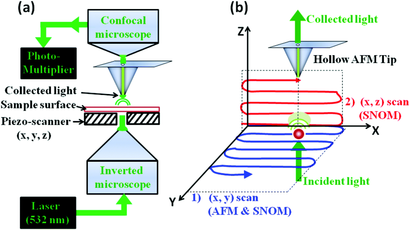 | ||
| Fig. 1 (a) Schematic of collection mode operation of the Witec Alpha 300S system we used for the 3D-SNOM study of Cu-NPs. The piezo-scanner can be manipulated to move in any of the three x, y, z directions. (b) Schematic diagram of the 3D SNOM configuration for measurements of topography and light scattering from Cu-NPs. Collection-mode and topography images are simultaneously obtained from an (x, y) AFM/SNOM scan at z = 0 while an (x, z) SNOM cross-section scan at y = const. is used to obtain the position of light scattered by the nanoparticles at different heights from the sample surface. | ||
2. Results and discussion
2.1 Samples used in this study
A distinct advantage of our method for growing Cu-NPs is that the direct-current biased, RF magnetron sputtering system in which our random arrays of Cu-NPs have been deposited and annealed (see the Experimental section for details) is directly attached to an inert-atmosphere glove box in which the samples can be analyzed and encapsulated with minimal oxygen exposure. Organic solar cell fabrication was also carried out in the same glove box, which is equipped with a built-in spin coater and an AM 1.5 solar simulator for device testing. The aperture-type scanning near-field optical microscope used for 3D-SNOM characterization is also located inside a sealed enclosure that can be filled with an inert gas, and in which samples can be transferred from the glove box in sealed bags. In order to demonstrate the importance of minimizing oxygen contamination of our Cu-NP samples, we investigated the degree of oxidation of Cu-NPs when annealed in air as well as in our nitrogen-filled glove box. The energy dispersive X-ray (EDX) spectra of two Cu-NP samples, annealed at 300 °C in air and in the glove box, as well as the reference as-deposited sample are displayed in Fig. 2, panels (a), (b) and (c), respectively. This sample was sputtered on the Si substrate for 3 minutes at 75 W RF power, 0 V dc bias and 9 Pa Ar pressure and divided into two parts that were annealed separately. | ||
| Fig. 2 EDX spectra showing the composition of Cu-NPs annealed at 300 °C for 1 h (a) in the glove box, and (b) in air. (c) EDX of reference as-grown Cu-NPs. (d) Comparison of the elemental composition from panels (a), (b) and (c). (e) Transmittance of Cu-NPs, as grown and annealed under different environmental conditions. | ||
The ratio of atomic contents of O and Cu (Fig. 2, panel d) shows that annealing in air led to severe oxidation of the Cu-NPs, while the O level was below the detection threshold (<1 at%) for the sample that was entirely annealed and treated inside the glove box. Fig. 2, panel (e), shows the optical transmission spectra of these samples. A dip centered at λp = 552 ± 5 nm, that can be assigned to resonant plasmon excitation,25,26 is evident in the transmission spectrum of the sample annealed and treated in the glove box, while it is undetectable in the air-annealed sample as a result of surface oxidation.27 On the other hand, the transmittance of the reference as-deposited Cu-NPs shows an enhancement (i.e. a peak in transmittance)28which is opposite to plasmonic enhancement (i.e. a dip in transmittance, corresponding to a peak in reflectance). The transmittance enhancement corresponds to metallic behavior of this sample; the morphology of the Cu-NPs presented in the following paragraph shows that the nanoparticles are highly inter-connected.
Fig. 3 shows the atomic force microscopy (AFM) images of the samples previously discussed in Fig. 2. Panel (a) shows the morphology of the sample prior to annealing, with a fine distribution of interconnected Cu-NPs that gave rise to a transmittance peak, as shown in Fig. 2e. Annealing in air (Fig. 3b) did not significantly alter the morphology of the sample. Although the Cu-NP diameter grows from 54 ± 5 nm to 61 ± 5 nm due to nucleation effects, particles are still interconnected and no plasmon-related feature was noticed in the optical transmission spectrum in Fig. 2e due to significant oxidation. Conversely, a more significant nucleation occurs upon annealing the sample in the glove box (Fig. 3c), with well separated and oxygen-free nanoparticles of 73 ± 2 nm in diameter. This demonstrates that, by growing our samples in an UHV deposition system attached to a glove box, we are able to completely overcome the effects of oxidation and to produce random arrays of Cu-NPs of suitable quality for nanoplasmonics. More experimental evidence on the nucleation of these particles, including the scanning electron microscopy images and particle distributions under different experimental conditions, can be found in the ESI.†
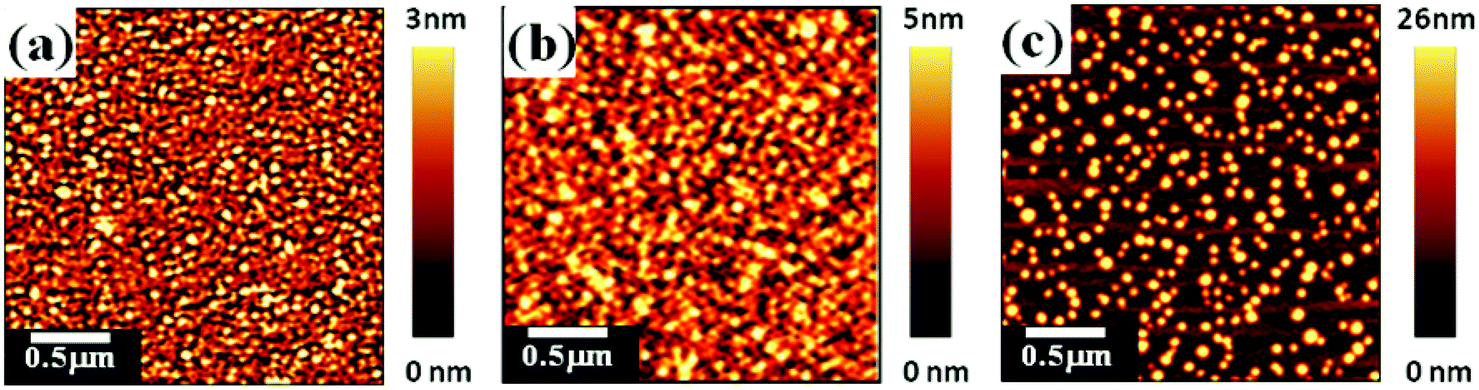 | ||
| Fig. 3 AFM topography images of (a) as-deposited, (b) air-annealed and (c) glove box annealed Cu-NPs. Thermal annealing was at 300 °C for 1 hour. | ||
In addition to thermal annealing of interconnected Cu-NPs, it was also possible to initiate further nucleation by island formation during sputtering, also known as Volmer–Weber growth29 without any post-annealing process. In order to identify the optimal growth conditions for random arrays of Cu-NPs for plasmonic photovoltaic applications, we varied the Ar partial pressure in the chamber from 9 Pa to 23 Pa and sputtered a set of samples at −400 V dc negative bias voltage. External negative bias of the sample is essential to decrease the deposition rate and favor the process of nucleation during the sputtering deposition, thus promoting Volmer–Weber growth of individual Cu-NPs rather than interconnected particles.29 The average particle diameter increased from 58 ± 10 nm to 95 ± 10 nm with increasing chamber pressure. A complete characterization of this set of samples including AFM images, optical transmission spectra, collection-mode SNOM images and 3D-SNOM profiles of forward-scattered light is reported in the ESI.†
2.2 3D-SNOM Imaging
Fig. 4 shows a typical example of one of the 3D-SNOM images obtained from the setup reported in Fig. 1, which shows the random system of Cu-NP grown at 12 Pa Ar pressure. The AFM image in panel (a) corresponds to the collection-mode SNOM image shown in panel (b), in which yellow pixels indicate regions from which a larger intensity of light is forward-scattered and collected from the tip aperture and black pixels indicate no light being collected. From Fig. 4b, it can be observed that at z ≈ 0, in the proximity of the sample surface, the intensity of light forward-scattered by the bare glass substrate is significantly lower than the intensity of light scattered by the Cu-NPs. As can be observed from Fig. 4a and 4b, the Cu-NP size cannot be considered to be much smaller than the illumination wavelength, λ. Therefore, when light interacts with these particles, the scattered electric field is not purely dipolar in nature, but is formed by an infinite superposition of multipoles.6 | ||
| Fig. 4 (a) Topographic and (b) optical images obtained simultaneously from SNOM measurements on Cu-NPs sputtered at 12 Pa chamber pressure. (c) Typical (x, z) SNOM intensity mapping performed along the A–A′ cross-section shown in panel (b) and (d) the intensity profile showing the positions of constructive (maxima) and destructive (minima) interference of light scattered from Cu-NPs. | ||
According to Mie theory, the multipolar nature of the scattered field is expected to manifest itself with the fact that the field intensity undergoes a number of oscillations, with maxima and minima at specific distances z, from the surface of the particles.30–33 Experimentally, these oscillations are clearly visible in Fig. 4c that represents a (x, z) SNOM scan of the line at y = const. indicated by letters A and A′ in Fig. 4b. No oscillations are visible if a bare glass substrate is scanned, which confirms that the forward-scattered near field that produces them must be attributed to the Cu-NPs. From Fig. 4c, it can also be noted that the light intensity is relatively uniform along the x-axis, with a relatively lower intensity for the corresponding largest particles. This is a consequence of the fact that even in this sample, in which the Cu-NPs are relatively sparse, the inter-particle distances are not significantly larger than a wavelength and, therefore, the Cu-NPs cannot be considered to be isolated. Fig. 4d shows the integrated intensity of forward-scattered light along the A–A′ cross-section. Maxima corresponding to constructive interference and minima corresponding to destructive interference are clearly visible. It can be seen that for this specific sample, the first maximum of forward-scattered light intensity was observed at Δz = 1200 nm above the glass surface, while the absolute maximum occurs at about Δz = 4400 nm, after which the intensity of scattered light drops to very low values as can be expected from the poor green light transmittance of Cu-NPs in the far field.13
Using this very same procedure, we performed 3D-SNOM scans on random arrays of Cu-NPs of different diameters, obtained from a set of samples deposited at increasing Ar pressures from 9 to 23 Pa (see the ESI† for detailed characterization). In Fig. 5 we show the variation of the first maximum of forward-scattered light intensity as a function of the average particle diameter and we observe that the light scattered from Cu-NPs with a larger diameter is more closely coupled to the surface of the sample than in smaller Cu-NPs. For instance, Cu-NPs with 95 ± 10 nm diameter shows scattered wave peaks at Δz1-max = 220 ± 50 nm, compared to Δz1-max = 1400 ± 100 nm for the particles with 58 ± 10 nm diameter. This can be attributed to the dependence on the particle size of the cross-sections for near-field optical absorption and scattering of light.5–7 The scattering cross-section is proportional to the square of the nanoparticle volume34 and, subsequently, for sufficiently large nanoparticles it can be considered to be much greater than the cross-section for optical absorption. Therefore, for Cu-NPs with a diameter greater than 80 nm, multipolar effects due to Mie scattering manifest themselves as strong coupling of the scattered waves in the vicinity of the NP surface.
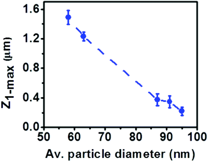 | ||
| Fig. 5 Variation of the scattered wave peak position with Cu-NP diameters. Z1-max represents the first significant peak intensity position of the scattered light obtained from (x, z) SNOM intensity profiles. The error bar corresponds to the standard deviation of 6 different intensity plots obtained from the SNOM map. | ||
For any particle diameters, the values of Δz1-max measured by us are too large to use the radiation that is forward scattered by Cu-NPs in the near-field for harvesting light in organic thin film solar cells if the active layer is immediately overlaid in contact with the nanoparticle array. Typically, organic solar devices are no thicker than 200 nm to minimize recombination of charges due to the high resistivity in the active layers.35,36 Decreasing the device thickness to a few hundred nanometers or less is also required to overcome recombination due to the short diffusion length of excitons generated within the active layer of the cell. As such, light absorption is generally limited by the thickness of the active layer. In order to use Cu-NPs for increasing the organic solar cell performance, it is essential to position the active layer at a distance Δzi-max at which the maximum intensity of light is forward-scattered, for efficient concentration of light into the device. These considerations mean that it would be beneficial to employ dielectric materials for which the desired scattering effects are still present but for which surface plasmon resonances do not occur.
We explored the prospects of this concept by developing a more structured plasmonic architecture in which a SiO2 thin film, sputtered in the same chamber used to prepare our Cu-NPs, functions as a spacer (see the ESI† for the detailed sputtering operation of the glass target). The AFM images, x–y SNOM images and 3D-SNOM images obtained with 100 nm diameter Cu-NPs with a 200 nm SiO2 spacer and without a spacer are reported in Fig. 6a–c and 6d–f, respectively. On the one hand, from the AFM image in panel (a), it can be observed that the surface of the sample is entirely flat after sputtering the SiO2 spacer and the Cu-NPs are entirely embedded in SiO2; on the other hand, the x–y transmission SNOM image in panel (b) clearly reveals the presence of Cu-NPs below the sample surface in this case. Conversely, in the absence of the spacer, Cu-NPs are visible at the very same locations in the AFM (panel d) and the x–y transmission SNOM image (panel d) in Fig. 6.
 | ||
| Fig. 6 (a) Topography, (b) the corresponding optical image and (c) SNOM (x, z) intensity mapping along the A–A′ cross-section for the Cu-NP/SiO2 spacer. The flatness of the topographic image is an indication that Cu-NPs are completely embedded in the 200 nm SiO2 spacer. Also shown are (d) topography, (e) the corresponding optical image and (f) SNOM (x, z) intensity map for the reference bare Cu-NPs on the glass substrate. | ||
More interesting results arise from the comparison of the 3D-SNOM images with and without a spacer, which are presented in panels (c) and (f), respectively. In the presence of the spacer, we observe a broad region of constructive interference of forward-scattered light, from zero to approximately 550 nm in the vicinity of the SiO2 surface. This broad enhancement region may be assigned to coupling of plane waves normally incident to the SiO2 surface with laterally propagating waves parallel to the SiO2 surface, which results in the introduction of a lateral wave vector component.37 Superposition of the lateral and normal components of the wave vector may also lead to the increased intensity of the scattered light in addition to constructive interference in the normally incident wave. These results indicate that this architecture is extremely promising for building a near-field plasmon-enhanced solar cell on top of its surface. Conversely, in the absence of the spacer, a destructive interference peak is located at approximately 160 ± 30 nm from the sample surface, which results from considerable near-field depletion in the region at which the active layer of a solar cell would be placed in this case. Fig. 7a shows the intensity profile of light scattered in the near-field along the z-axis, extracted from the 3D-SNOM images in Fig. 6c and f. It can be observed that, in addition to a broader constructive interference peak, the structure with the spacer produces a significantly higher intensity of forward-scattered light.
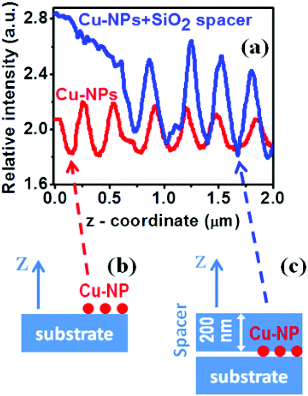 | ||
| Fig. 7 (a) The intensity profiles showing the positions of the scattered wave enhancements from Cu-NP/SiO2 and the reference bare Cu-NPs measured by our (x, z) SNOM technique. A schematic diagram showing samples of Cu-NPs (b) without and (c) with a 200 nm SiO2 spacer, with arrows pointing to the corresponding intensity profiles. | ||
2.3 Solar cell fabrication and testing
In order to demonstrate the critical importance of our 3D-SNOM method in designing nanostructures for plasmonic enhancement, we have built and tested two identical bulk heterojunction (BHJ) organic solar cells on top of our plasmonic architectures presented in Fig. 7b and c, with and without a 200 nm SiO2 spacer on top of Cu-NPs. Solar cell fabrication was carried out in the glove box that was directly attached to the sputtering system used to deposit the Cu-NPs and the SiO2 spacer, without direct exposure of the sample to air. A 100 nm indium-tin oxide (ITO) thin film was spun directly on top of the two surfaces, with and without the spacer, from a colloidal suspension of ITO in isopropanol. The as-spun samples were subsequently annealed at 400 °C, a temperature that does not affect the morphology of Cu-NPs. This thermal treatment is essential for the colloidal ITO to coalesce and form a continuous ITO thin film of 150 Ω sq−1 sheet resistance. Anhydrous PEDOT:PSS in isopropanol was spun on the top of ITO to form a 30 nm hole transport layer. The solar cell active layer consisted of a 120 nm mixture of regioregular poly(3-hexylthiophene-2,5-diyl) (P3HT) and [6,6]-phenyl-C61-butyric acid methyl ester (PCBM) spun from chlorobenzene.Bilayer metallic contacts of calcium (20 nm) and aluminum (100 nm) were fabricated in a thermal evaporator that was also installed in the same chamber housing the sputtering system, which resulted in four complete solar cells assembled on top of each of our four plasmonic architectures. The schematic of these devices is shown in Fig. 8a and b, respectively.
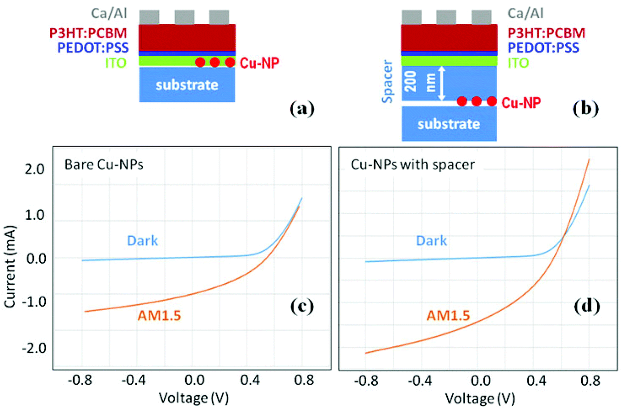 | ||
| Fig. 8 The scheme of (a) the reference solar cell of bare Cu-NPs without a spacer and (b) the solar cell architecture designed with the aid of our 3D-SNOM results that includes a 200 nm SiO2 spacer. I–V characteristics of the solar cells with a Cu-NP plasmonic layer (c) without and (d) with a spacer between Cu-NPs and the ITO-P3HT/PCBM organic active layer. | ||
Device testing was also carried out in the glove box and the current–voltage (I–V) curves produced are shown in Fig. 8c and d, respectively. It can be observed that, although the dark characteristics of the two devices are basically the same, a significantly larger photocurrent could be extracted from the devices built on the architecture with the spacer, which produced an average short-circuit current Isc = 1.44 mA, more than twice the value (Isc = 0.67 mA) obtained in the absence of the spacer. Conversely, the open circuit voltage (Voc ≈ 0.56 ± 0.02 V) and fill factor (52 ± 2%) of the two types of devices did not show any noticeable differences. These results are a strong indication of the fact that the resulting increase in AM 1.5 photoconversion efficiency (η = 3.08% on average in the presence of the spacer vs. η = 1.38% in the absence of the spacer) is a consequence of the enhancement of light conveyed within the active layer of the device due to near-field radiation forward-scattered by Cu-NPs. In order to further substantiate these findings an identical control cell was also fabricated without any underlying array of Cu-NPs, which resulted in an efficiency (η = 2.45%) that was intermediate between the two cases, further corroborating the usefulness of our 3D-SNOM method for effectively identifying specific conditions for plasmonic solar cell enhancement.
3. Conclusion
Copper nanoparticles were deposited using a radio frequency (RF) sputtering system for use as a plasmonic enhancement layer in thin film organic solar cells. Our deposition system, which comprises a coupled sputtering chamber, thermal evaporator and glove box, was specifically set up to achieve the deposition of contaminant-free NPs in the high vacuum environment, while the storage and manipulation are carried out under an inert atmosphere in the glove box. Cu-NPs of different diameters were obtained by varying the deposition chamber pressure and were used to study the scattering phenomenon arising from the light interaction with the nanoparticles.By introducing a novel 3D scanning near-field optical microscope technique, we obtained the various positions of constructive interference peaks of plasmonic waves arising from multipolar contributions to the scattering cross-section by Cu-NP ensembles. The best coupling of the scattered light to the sample surface was achieved by incorporating a 200 nm SiO2 spacer between the Cu-NPs and the sample surface. With this configuration, the scattered light waves extended up to 500 nm from the Cu-NP/SiO2 surface. The observed improvement in the scattering enhancement from Cu-NP/SiO2 surfaces is ideal for the improved performance in plasmonic devices such as thin film solar cells that are normally no more than 200 nm in thickness.
4. Experimental details
The Cu-NPs we studied were deposited by Radio Frequency (RF) magnetron sputtering of a copper target with argon ions in a vacuum chamber. The deposition chamber is attached to a nitrogen-filled glove box through a gate valve interconnect that allows for easy access to the chamber (see the ESI† for detailed description of our deposition system). Cu-NPs of different sizes were deposited on microscope glasses with a RF power of 75 W for 3 minutes at increasing chamber pressures from 9 Pa to 23 Pa.In order to verify the effect of oxidation on thermally treated Cu-NPs, we performed energy dispersive X-ray spectroscopy (EDX) analysis of the samples deposited under the same conditions but annealed in a different environment using a LEO (Zeiss) 1540 field emission scanning electron microscope (SEM). This sample was sputtered on the Si substrate for 3 minutes at 75 W RF power, 0 V dc bias voltage and 9 Pa Ar pressure and divided into two parts that were annealed separately at 300 °C for 1 hour. The glove-box annealed sample was taken out immediately before being measured with a dwell time no more than 10 minutes before being admitted to the SEM/EDX chamber. The UV-VIS transmittance of the NPs was measured at normal incidence in the range of wavelengths between 350 nm and 800 nm using a Varian DMS80 spectrophotometer. The transmittance data were obtained at a step scan rate of 10 nm per second.
Near field optical study and morphological mapping on the nanoscale were performed using a Witec Alpha 300S atomic force microscope. The Witec Alfa 300S, an aperture-type, AFM-integrated SNOM instrument can be used to record SNOM images and, simultaneously, AFM topographic images of a sample. The system can record SNOM images in ‘transmission mode’ or in ‘collection mode’ that differ in the way the sample is illuminated and the scattered light is collected. In the collection mode operation described schematically in Fig. 1a, light from a 532 nm green laser operated up to 50 mW (Excelsior, Spectra Physics Inc., serial no. 10398) is directed, by a system of optical fibers, into an inverted microscope, and the optical response of the sample is collected by the nanohole (d ≈ 80 nm) located at the end of an AFM hollow tip, mounted below a high-resolution confocal microscope. The collected light is subsequently launched via the confocal microscope into an optical fiber that is connected to a photomultiplier tube (U-68000, Hamamatsu) operating in photon-counting mode. The sample is positioned on a 100 × 100 μm piezo-scanner that has a maximum excursion of 10 μm in the z-direction. In addition, the mechanical arm on which the confocal microscope is mounted can also be moved in the z-direction for optimizing the focal plane at the level of the AFM tip. If the hollow tip is sufficiently close to the sample surface, only the near-field optical response from the sample surface will be collected. However, if the hollow tip is lifted up at a controlled distance z from a nanoparticle that is located at the sample surface, all of the other normal modes representing the propagating component of the scattered waves can be detected.
In our SNOM collection mode operation, the sample surface was scanned along the (x, y) plane at z = 0, or in the (x, z) direction at y = constant, in order to obtain relevant information about the amount of light scattered by the particle at a nonzero distance from its surface, as demonstrated in Fig. 1b. With this three-dimensional optical imaging procedure, specifically designed for this study, the collection mode SNOM analysis was carried out first to obtain the (x, y) nano-optical and topographic (contact-mode AFM) images of Cu-NPs, which were recorded simultaneously. We then chose a line at y = const. from the (x, y) images and changed the distance z from the tip to the sample surface. This can be done reproducibly because the piezo-scanner stage on which the sample is mounted allows us to control the sample–tip distance with ±1 nm reproducibility.
The preparation of two identical organic solar cells with and without a 200 nm SiO2 spacer on top of Cu-NPs was carried out following the same procedure that was reported previously.38 Both the fabrication and device testing were performed in the glove-box, loaded with high-purity nitrogen, with oxygen and moisture levels less than 5 ppm. A 100 nm indium-tin oxide (ITO) thin film was spun directly on top of the two surfaces, with and without the spacer, from a colloidal suspension of ITO in isopropanol. The samples were then fast-annealed at 400 °C for 5 min. An anhydrous Poly(3,4-Ethylene Di-Oxy-Thiophene):Poly-Styrene Sulfonate thin film (PEDOT:PSS, Aldrich cat. no. 483095) in isopropanol was spun at 3000 rpm on the top of ITO to form a 30 nm hole transport layer, and then baked on a hot plate at 140 °C for 30 min. The solar cell active layers were assembled by spinning on the top of PEDOT:PSS a mixture (15![[thin space (1/6-em)]](https://www.rsc.org/images/entities/char_2009.gif) :15 mg) of regioregular poly(3-hexylthiophene-2,5-diyl) (P3HT) and [6,6]-phenyl-C61-butyric acid methyl ester (PCBM) (Aldrich, cat no. 698989 and 684430, respectively) in chlorobenzene, followed by thermal annealing at 120 °C for 15 min.
:15 mg) of regioregular poly(3-hexylthiophene-2,5-diyl) (P3HT) and [6,6]-phenyl-C61-butyric acid methyl ester (PCBM) (Aldrich, cat no. 698989 and 684430, respectively) in chlorobenzene, followed by thermal annealing at 120 °C for 15 min.
The solar cells were then transferred into the deposition chamber for thermal evaporation of Ca/Al bilayer backing electrodes. The metallic contacts (20 nm Ca thickness and 100 nm Al thickness, measured using a Sycom STM-2 thickness monitor) were evaporated on each solar cell using a patterned shadow mask,38 resulting in a device area of 0.245 cm2 each. The solar cell I–V characteristics were measured directly in the glove box using a Newport 9600 AM 1.5 solar simulator at 1 sun. The solar simulator was calibrated using a Sciencetech SC-LT standard cell with certification accredited by the National Institute of Standards and Technology (ISO-17025).
Acknowledgements
This work was supported through the Natural Sciences and Engineering Research Council of Canada Discovery Grant program. GF acknowledges a Canada Research Chair in Carbon-based nanomaterials and Nanooptoelectronics and financial support from the Canada Foundation for Innovation (CFI). HY acknowledges a MITACS Globalink summer award.Notes and references
- K. R. Catchpole and A. Polman, Opt. Express, 2008, 16, 21793 CrossRef CAS.
- X. Gu, T. Qiu, W. Zhang and P. K. Chu, Nanoscale Res. Lett., 2011, 6, 199 CrossRef PubMed.
- E. E. Bedford, J. Spadavecchia, C. M. Pradier and F. X. Gu, Macromol. Biosci., 2012, 12, 724 CrossRef CAS PubMed.
- D. Courjon and C. Bainier, Rep. Prog. Phys., 1994, 57, 989 CrossRef.
- M. A. Garcia, J. Phys. D: Appl. Phys., 2011, 44, 283001 CrossRef.
- C. F. Bohren and D. R. Huffman, Absorption and Scattering of Light by Small Particles, Wiley, New York, 1983 Search PubMed.
- U. Kreibig and M. Vollmer, Optical Properties of Metal Clusters, Springer Series in Material Science, 25, Springer, Berlin, 1995 Search PubMed.
- G. Mie, Ann. Phys., 1908, 25, 377 CrossRef CAS.
- U. Kreibig, B. Schmitz, H. D. Breuer and H. D. Breuer, Phys. Rev. B: Condens. Matter, 1987, 36, 5027 CrossRef.
- M. A. Garcia, S. Paje and J. Llopis, Chem. Phys. Lett., 1999, 315, 313 CrossRef CAS.
- K. R. Catchpole and A. Polman, Appl. Phys. Lett., 2008, 93, 191113 CrossRef PubMed.
- H. Raether, Tracts in Modern Physics, Springer, 1980, 88,4 Search PubMed.
- H. Ehrenreich and H. Philipp, Phys. Rev., 1962, 128, 1622 CrossRef CAS.
- S. Pillai, K. R. Catchpole, T. Trupke and M. A. Green, J. Appl. Phys., 2007, 101, 093105 CrossRef PubMed.
- S. Pillai, K. R. Catchpole, T. Trupke, G. Zhang, J. Zhao and M. A. Green, Appl. Phys. Lett., 2006, 88, 161102 CrossRef PubMed.
- V. I. Belotelov, L. E. Kreilkamp, I. A. Akimov, A. N. Kalish, D. A. Bykov, S. Kasture, V. J. Yallapragada, A. V. Gopal, A. M. Grishin, S. I. Khartsev, M. Nur-E-Alam, M. Vasiliev, L. L. Doskolovich, D. R. Yakovlev, K. Alameh, A. K. Zvezdin and M. Bayer, Nat. Commun., 2013, 4, 2128 CAS.
- Y. Song, W. Yin, Y. H. Wang, J. P. Zhang, Y. Wang, R. Wang, J. Han, W. Wang, S. V. Nair and H. E. Ruda, Sci. Rep., 2014, 4, 4991 Search PubMed.
- Y. Song, Y. Wang, B. B. Li, C. Fernandes and H. E. Ruda, Nanoscale, 2013, 5, 6779 RSC.
- Y. Song, R. Li, Q. Sun and P. Jin, Chem. Eng. J., 2011, 168, 477 CrossRef CAS PubMed.
- I. Lisiecki, F. Billoudet and M. P. Pileni, J. Phys. Chem., 1996, 100, 4160 CrossRef CAS.
- R. V. Kumar, Y. Mastai, Y. Diamant and A. Gedanken, J. Mater. Chem., 2001, 11, 1209 RSC.
- S. Schiller, K. Goedicke and J. Reschke, Surf. Coat. Technol., 1993, 61, 331 CrossRef CAS.
- L. Antonio and H. Steven, Handbook of Photovoltaic Science and Engineering, John Wiley & Sons, United Kingdom, 2nd edn, 2011 Search PubMed.
- B. Hecht, B. Sick, U. P. Wild, V. Deckert, R. Zenobi, O. J. F. Martin and D. W. Pohl, J. Chem. Phys., 2000, 112(18), 7761 CrossRef CAS PubMed.
- V. Halte and J. Y. Bigot, http://www-ipcms.u-strasbg.fr/spip.php?rubrique311.
- E. D. Mozrzymas and P. Bieganski, Appl. Opt., 1993, 32(13), 2345 CrossRef PubMed.
- G. H. Chan, J. Zhao, E. M. Hicks, G. C. Schatz and R. P. V. Duyne, Nano Lett., 2007, 7(7), 1947 CrossRef CAS.
- N. Bonod, S. Enoch, L. Li, E. Popov and M. Neviere, Opt. Express., 2003, 11(5), 482 CrossRef CAS.
- G. Cao and Y. Wang, Nanostructures and Nanomaterials, World Scientific, 2011, pp. 230–231 Search PubMed.
- B. Hecht, H. Bielefeldt, L. Novotny, Y. Inouye and D. W. Pohl, Phys. Rev. Lett., 1996, 77(9), 1889 CrossRef CAS.
- S. I. Bozhevolnyi, B. Vohnsen, I. Smolyaninov and A. V. Zayats, Opt. Commun., 1995, 117, 417 CrossRef CAS.
- D. Pohl, W. Denk and M. Lanz, Appl. Phys. Lett., 1984, 44, 651 CrossRef PubMed.
- O. Muskens, D. Christofilos, N. D. Fatti and F. Vallee, J. Opt. A: Pure Appl. Opt., 2006, 8, S264 CrossRef.
- O. Stenzel, A. Stendal, K. Voigtsberger and C. V. Borczyskowski, Sol. Energy Mater. Sol. Cells, 1995, 37, 337 CrossRef CAS.
- W. Westphalen, U. Kreibig, J. Rostalski, H. Luth and D. Meissner, Sol. Energy Mater. Sol. Cells, 2000, 61, 97 CrossRef.
- E. T. Yu, D. Derkacs, S. H. Lim, P. Matheu and D. M. Schaadt, Proc. SPIE, 2008, 7033, 70331 CrossRef PubMed.
- H. R. Stuart and D. G. Hall, Appl. Phys. Lett., 1996, 69(16), 2327 CrossRef CAS PubMed.
- R. Bauld, M. Hesari, M. S. Workentin and G. Fanchini, Nanoscale, 2014, 6, 7570 RSC.
Footnote |
| † Electronic supplementary information (ESI) available: Detailed description of the deposition system and a complete characterization of the set of samples deposited at different chamber pressures, including AFM images, optical transmission spectra, collection-mode SNOM images and 3D-SNOM profiles of forward-scattered light. See DOI: 10.1039/c4nr05094k |
| This journal is © The Royal Society of Chemistry 2015 |