Scale-up of oCVD: large-area conductive polymer thin films for next-generation electronics
Peter
Kovacik
,
Gabriella del
Hierro
,
William
Livernois
and
Karen K.
Gleason
*
Department of Chemical Engineering, Massachusetts Institute of Technology, Cambridge, Massachusetts 02139, USA. E-mail: kkg@mit.edu
First published on 2nd January 2015
Abstract
Scale up of oxidative chemical vapor deposition (oCVD) is demonstrated. Transparent conductive poly(3,4-ethylenedioxythiophene) (PEDOT) films were deposited with excellent thickness and compositional uniformity across large areas (exceeding 20 × 30 cm) for the first time. The optical and electronic properties of PEDOT achieved in small scale reactors were also achieved in this large format, as desired for enabling large-scale application of oCVD PEDOT in organic solar cells or organic light-emitting displays at commercially feasible cost. Moreover, conformal and substrate-independent character of oCVD was utilized to fabricate conductive textiles via patterned deposition on t-shirts. The conductivities of the textile up to 32 S cm−1 are among the highest reported for a vapor- or solution-based PEDOT coating, while at the same time exhibiting excellent mechanical durability demonstrated through extensive twisting, stretching, and washing in H2O. Such functionality combined with deposition versatility opens up novel opportunities for integration of organic electronics into everyday life.
Conceptual insightsThis work demonstrates scalability of oxidative chemical vapor deposition (oCVD) as a method for fabrication of conductive and semiconductive polymer thin films. oCVD is a solvent-free method which yields high-quality conformal films applicable to any substrate. Excellent functionality of the films combined with the low deposition temperature (<200 °C) and mild vacuum requirements (>10 Pa) make this technique economically feasible and suitable for various applications, extending its versatility beyond standard vapor- and solution-based deposition techniques. For example, film conformality allows deposition on rough and fibrous materials such as paper, textiles, or wood. Transfer of functional nanoscale coatings to ‘scientifically’ unconventional materials and objects, as demonstrated in this work, is an important step towards integration of organic electronics into everyday life. |
Introduction
Integration of organic electronics into everyday life relies on innovative technologies and their scalable fabrication. A necessary balance is required between performance and cost of the technology, as well as its applicability to novel and unconventional device architectures. Polymeric conductors, especially poly(3,4-ethylenedioxythiophene) (PEDOT), have been critical in demonstrating a myriad of application avenues otherwise inaccessible using inorganic nanostructured materials.1 Commonly used soluble PEDOT:poly(styrenesulfonate) (PSS) provides good electrical and mechanical properties for a relatively low cost.2 However, many drawbacks hinder its further applications, such as acidity, hygroscopic character, poor stability,3,4 and processing limitations restricting its deposition only to a limited type of surfaces.5 Some of the issues can be addressed by removal of PSS from the deposited film.6 Coating of micro- or nano-textured substrates by PEDOT solutions nevertheless remains a substantial challenge due to de-wetting, liquid thinning, and surface tension effects. Large-scale deposition can be achieved by various methods, such as spray7 or slot-die8 coating, but the solution processing inherently requires modification of the PEDOT:PSS viscosity and surface tension for each specific deposition technique.9 This often results in compromise in other properties, particularly conductivity.Oxidative chemical vapor deposition (oCVD) has emerged as an effective technique for simultaneous synthesis and deposition of conjugated polymers.10 The deposited films are conformal and applicable to any type of substrate. Highly conductive oCVD PEDOT films have been successfully integrated in many advanced device architectures.11,12 These include transparent electrodes for organic solar cells deposited on light-trapping surfaces or a standard office paper.13,14 The conformality, substrate independence, and good control over the film parameters have all proven essential for complex nanoscale interfaces required for the next-generation electronics.
Different CVD methods have not only illustrated superior performance and versatility, but also cost-effectiveness and scalability.15 CVD techniques with various degrees of complexity are routinely used in industry, ranging from fabrication of microchip technology to low-cost barrier coating of plastic bottles. Initiated chemical vapor deposition (iCVD), a method closely related to oCVD, has been scaled up in batch16 as well as roll-to-roll mode,17 and has already provided multiple commercial solutions.18 In this study we demonstrate successful scale up of oCVD method via batch processing of large-area samples. We fabricate transparent and conductive PEDOT films with high uniformity across an area covering size of A4 sheet or 15.4′′ display. We combine large-scale deposition with the method's conformality and substrate-independence to produce patterned conductive textiles with excellent endurance properties. Overall, this study illustrates potential of oCVD as a scalable and commercially feasible method with unique deposition capabilities.
Results & discussion
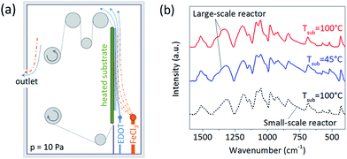
Oxidative CVD polymerization results from surface reaction of the monomer and oxidant flows,19–21 here 3,4-ethylenedioxythiophene (EDOT) and iron chloride (FeCl3), respectively. Manifold sources were therefore employed for both monomer and oxidant. Their adjacent placement allowed sufficient mixing of the precursors and formation of a reaction zone along the substrate, as pre-modeled by computational fluid dynamics calculations. Uniform upward direction of the flows was aided by blocking the gaps on side and bottom of the heating plate. The oCVD reactor was designed for roll-to-roll (R2R) operation with a roll width of 12′′ (∼30 cm). As a first step, the goal of this work was to achieve the desired uniformity on stationary substrates positioned in the active zone where deposition would occur in R2R operation. Particular consideration was given to lateral uniformity of the batch deposition, since R2R mode would induce spatial averaging in the orthogonal direction due to movement of the substrate. The simplified reactor layout is depicted in Fig. 1a. The film deposition was conducted under fully controlled parameters, such as the chamber pressure (10 Pa), flow of the precursors (25 ± 5 sccm), and temperature of the substrate (45 and 100 °C).Conductivity of PEDOT exhibits a strong dependence on the substrate temperature.19,20 As shown previously, increasing temperature leads to improved conjugation, crystallinity, and doping concentrations in the films. Hence, we studied deposition of PEDOT at two different substrate temperatures, 45 °C and 100 °C. Fig. 1b compares FTIR spectra of the films to a PEDOT sample deposited in the small-scale reactor at the temperature of 100 °C. The spectral analysis revealed similarity of all PEDOT samples, confirming successful synthesis and deposition of the polymer in the large-scale reactor. This includes characteristic broad peaks20 between 700 and 1450 cm−1 and strong presence of C![[double bond, length as m-dash]](https://www.rsc.org/images/entities/char_e001.gif) C double bond at 1520 cm−1. However, the FTIR spectra do not resolve any significant difference between the low- and high-temperature films. The range of conductivities of PEDOT was 0.2–15 S cm−1 for films deposited at 45 °C, and 50–180 S cm−1 for 100 °C (the ranges include variation in sample locations as well as different depositions). These values are similar to those of the films fabricated in the small-scale reactor under comparable deposition conditions.20 As expected, the conductivity was significantly improved with elevated temperature. This suggests that further enhancements can be made using even higher substrate temperatures.
C double bond at 1520 cm−1. However, the FTIR spectra do not resolve any significant difference between the low- and high-temperature films. The range of conductivities of PEDOT was 0.2–15 S cm−1 for films deposited at 45 °C, and 50–180 S cm−1 for 100 °C (the ranges include variation in sample locations as well as different depositions). These values are similar to those of the films fabricated in the small-scale reactor under comparable deposition conditions.20 As expected, the conductivity was significantly improved with elevated temperature. This suggests that further enhancements can be made using even higher substrate temperatures.
Transparency of a PEDOT film is important for application as a transparent conductive electrode in optoelectronics.22 Transmittance spectra of large-area PEDOT films were thus measured, with selected samples of different film thickness shown in Fig. 2a. The films show high transparency in the visible-light region and suitability for applications, such as organic photovoltaics (OPV) or organic light-emitting diode (OLED) devices. Since the transmittance is inversely proportional to the sheet resistance (Rs) of the material, a balance is required between these two to optimize the overall electrode performance. Their relation can be quantified as a figure of merit, defined by the ratio of the dc to optical conductivity. Fig. 2b plots transmittance vs. Rs of PEDOT for both substrate temperatures. The calculated dc/optical conductivity ratios are 0.3 for 45 °C and 1.6 for 100 °C. The ratio of 12 has been achieved for oCVD PEDOT using elevated substrate temperature and dopant exchange through rinsing in HBr.23 For example, FeCl3 residues play a role in the film crystallization process and lead to creation of negative charges that decrease the hole carrier density and conductivity.24 Efforts are hence under way to increase the figure of merit via further improvements in crystallinity and doping.
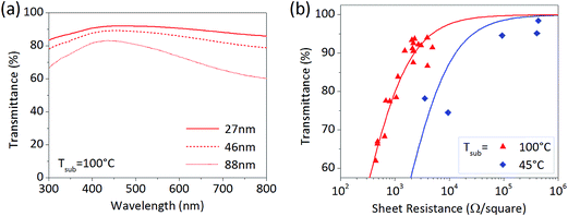 | ||
| Fig. 2 (a) Transmittance spectra of PEDOT films with different thickness deposited at substrate temperature Tsub = 100 °C in the large-scale reactor. (b) Transmittance T as a function of the sheet resistance Rs for PEDOT films at the substrate temperature of 45 °C (blue diamond) and 100 °C (red triangle). The data points are fitted using T vs. Rs theoretical dependence22 (red and blue lines). | ||
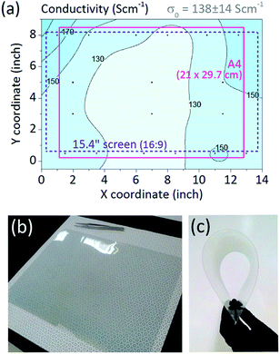
Scale-up of a deposition technique requires not only retention of the material's functional properties, but also their consistent transfer to a large scale. Uniformity of the oCVD PEDOT films was thus studied across an area of approximately 8.5 × 13′′ (∼21.5 × 33 cm), and at the temperature of 100 °C. The resulting 2D profile of conductivity is plotted in Fig. 3a. The average conductivity of PEDOT was 138 S cm−1 with deviation of only 10%, illustrating excellent material uniformity of the deposited polymer. The area can accommodate substrates for large-scale commercial devices, for example an A4-sized solar cell or a 15.4′′ widescreen laptop display. As a demonstration, flexible A4 Melinex PET sheet was coated by a transparent conductive layer of oCVD PEDOT, as shown in Fig. 3b and c. To note, the vertically oriented architecture of the reaction zone results in a slight vertical thickness gradient in the film. However, this occurs only for the batch deposition as the R2R mode would integrate the vertical axis through the movement of the substrate. In fact, the vertical thickness integration of the deposition zone revealed overall lateral deviation to be only 5.5% across 13′′ width. This satisfies uniformity requirements for 12′′ roll processed in R2R operation. Further improvements in lateral uniformity can be done through adjustment of the manifold nozzles for either of the sources.
Commercial viability of PEDOT films produced by R2R oCVD processing was estimated using an economic model from CVD manufacturer Aixtron.25 Cost of the deposited material was identified as one of the key factors influencing the price of the transparent conductive film. This is in accordance with the previous economic studies evaluating different thin-film technologies as alternatives to indium tin oxide (ITO).2,26–28 Since oCVD allows simultaneous synthesis and deposition of the polymer, multiple synthetic/processing steps can be avoided which are required for other materials systems. We estimate the price of the PEDOT films deposited in our reactor to be 0.2–1.0 $ per m2. The price range is comparable to PEDOT:PSS,2,28 and it is significantly lower than other systems, including ITO, carbon nanotubes, Ag grids, or Ag nanowires. Bulk cost of EDOT as well as improvement in deposition efficiency (>2%) would lead to further cost reductions (note, that the price does not include capital costs, cost of the substrate, or cost of energy required for processing).
For organic electronics to become ubiquitous it needs to be integrated into everyday materials and objects, and as a consequence allow novel technologies and open up new markets.29 Firstly, this involves a transfer of a technology from laboratory-favored substrates, such as glass or silicon, not only to smooth foils but also to rough paper, textiles, or potentially 3D objects. Secondly, this transfer should lead to a fully compatible system that preserves the original purpose or functionality of the object, for example an inexpensive technology on inexpensive paper, or a mechanically robust technology on strain-enduring clothing. oCVD has demonstrated functional films on paper10,19 and electrospun fibers,30 and in this work we extend the range of suitable substrates to textiles.
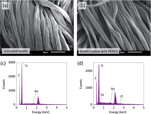
Smart textiles and wearable electronics are an area with enormous potential in human wellbeing.31 Different methods have been developed to produce electronic fabrics.32–35 These fall mainly in two categories – fabrication of individual functional fibers for textile weaving, and coating of functional materials on common pre-woven textiles. Although there are advantages to each method, the former group of techniques often requires more expensive and lower-throughput processing with a lack of patterning capabilities, while the latter group often suffers from mediocre performance and functionality as well as poor mechanical endurance. We show that oCVD coating of textiles allows achieving good performance together with mechanical endurance and pattern ability. Conductive PEDOT films were deposited on standard cotton/spandex textiles to demonstrate functional conformal coatings over large areas. Fig. 4a and b show SEM images of the fibers before and after the PEDOT deposition. Similarity of the textiles illustrates excellent conformal coverage of the fibers with thin film of the polymer. Presence of PEDOT was not only apparent from non-zero conductivity of the textile but also from energy-dispersive X-ray spectroscopy (EDS) analysis shown in Fig. 4c and d. The EDS spectra of coated fibers show elemental peaks of iron (Fe) at ∼0.7 keV and chloride (Cl) at ∼2.6 keV, both unreacted residues from oCVD polymerization. Sulfur (S) signal at ∼2.3 keV from PEDOT was unfortunately overlaid by that of gold (Au), which was used for coating of the samples to prevent beam-induced charging.
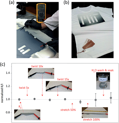
Coating quality shown in Fig. 4b is unparalleled to many other industrially scalable methods.36 For example, physical vapor deposition (PVD) results in a line-of-sight layer of the conductive material which is poorly connected and prone to delamination.37,38 Solution printing leads to an uneven coverage of the fibers due to wetting issues,39 moreover, by clogging the voids between the fibers40 it can compromise original functionality of the textile. Both techniques yield films with poor mechanical endurance. On the other hand, conformal character of oCVD PEDOT utilizes the film connectivity, does not alter functional properties of the textile, and allows robust response to mechanical stress. We found the sheet resistance of the fabricated PEDOT textile to be as low as 370 Ω per square, with the lower estimate for conductivity being >32 S cm−1 (the thickness of PEDOT on the fibers could not be accurately measured, but due to the film formation across the full depth of the fabric the coating thickness was likely lower than that on the reference flat substrate). To our best knowledge, this is the highest reported conductivity for a vapor- or solution-imprinted conductive textile based on PEDOT,41–46 comparable even to PEDOT fibers fabricated by wet-spinning.47–49 Since a conformal polymer thin film has a strong ability to absorb strain,45 the conductive PEDOT textile also exhibited excellent durability even under strenuous mechanical testing. As shown in Fig. 5c, resistance of the textile stayed almost unchanged despite the fabric being twisted to its limits (15 × 360°), stretched by as much as 100%, or washed and soaked in water for 5 min. Such mechanical durability is essential for application in smart clothing50 (to note, standardized washing tests are planned to ensure compliance with the industrial requirements).
Finally, patterning and customization of imprints is often desired to interconnect different functional devices/modules across the textile or to modify functionality (e.g. resistance) of the imprinted areas. This was demonstrated by depositing a masked MIT logo on a standard t-shirt, as shown in Fig. 5a and b. Modification of the imprint coverage was achieved via adjustment of the oxidant-manifold nozzles, while the patterning was done simply by taping off the letters. Increased patterning resolution could be achieved for instance by using localized physical compression.51 Analogous result for woven conductive fabrics would require cutting of different functional areas and sewing them on the t-shirt. We thus show that oCVD combines multiple benefits, allowing single-step fabrication of conductive and robust conductive films with simultaneous patterning and modification capabilities.
Conclusion
Oxidative CVD polymerization was scaled up and successfully applied to large-area flexible substrates. Custom-built roll-to-roll reactor was used to deposit conductive polymer PEDOT with conductivities comparable to those yielded by a small-scale reactor. The polymer retained the same chemical structure as on a small scale, as shown by FTIR, and excellent material's uniformity across an area of 8.5 × 13′′ (∼21.5 × 33 cm), as shown by conductivity measurements. Conductivity deviation of only 10% was achieved for stationary substrates with the lateral deviation of only 5.5%, rendering the technique suitable for R2R operation. Deposition in a continuous R2R mode is currently under investigation.Transparent conductive PEDOT coating was deposited on an A4-size plastic foil which demonstrates potential in organic optoelectronic devices, such as OLEDs and solar cells. The inherent conformality and substrate-independence of the method was further utilized to fabricate large-area patterned conductive textiles with outstanding mechanical endurance properties. This versatility extends the applicability of oCVD beyond standard vapor- and solution-based deposition techniques, and thus makes it a commercially attractive solution for various organic electronics applications.
Commercial viability was assessed using industrial CVD models, leading to $ per m2 cost of the PEDOT films that compares favorably to ITO, carbon nanotubes, Ag grids, or Ag nanowires, and similarly to PEDOT:PSS. As regards the commercial application, similar batch processing CVD methods have been successfully applied in other parts of industry.15 For example, plasma-impulse CVD produces extremely low-cost barrier coatings of plastic bottles at the speed of 40![[thin space (1/6-em)]](https://www.rsc.org/images/entities/char_2009.gif) 000 bottles per hour.52 This should encourage further interest in scale up of novel processing methods, such as oCVD, which can provide excellent coating capabilities at economically feasible cost.
000 bottles per hour.52 This should encourage further interest in scale up of novel processing methods, such as oCVD, which can provide excellent coating capabilities at economically feasible cost.
Experimental methods
The reactor used in the experiments is a custom modified R2R PECVD system from PLASMATech (model V-160GK-RT, volume 0.16 m3, maximum roll width ∼30 cm, and diameter ∼16 cm). A vertical stainless steel heating plate (45.7 cm tall × 43.2 cm wide × 0.6 cm thick) was heated by three horizontally-oriented strip heaters from Omega Engineering attached to the back side. Simplified side profile of the reactor is shown in Fig. 1a. Gaps at the side and bottom of the heating plate were blocked in order to direct the flow upwards along the substrate. Lateral uniformity was achieved using linear manifold sources. The monomer source was fabricated in-house, with 8 nozzles of variable diameter and the length of 16′′, equivalent to ∼40 cm. The oxidant source was custom-produced by SVT Associates, with 9 nozzles of variable diameter and the length of 15′′, equivalent to ∼36 cm. Both manifolds as well as the monomer delivery line were heated above the vaporization temperatures of the respective materials. The chamber was heated to approximately 60 °C.The polymer was synthesized using oxidative chemical vapor deposition19 during which the substrate was simultaneously exposed to vapors of 3,4-ethylenedioxythiophene (EDOT) monomer (TCI Chemicals, >98.0%) and FeCl3 oxidant (Sigma Aldrich, 99.99%). The evaporated monomer was delivered using the heated monomer manifold at the rate of 25 ± 5 sccm. The oxidant was evaporated from a resistively heated crucible at 160–200 °C and distributed by the oxidant manifold heated separately at 200–300 °C. The substrate was heated at 45 °C and 100 °C. The chamber pressure during the deposition was kept constant at 10 Pa. Deposition time was varied to achieve different film thicknesses. The PEDOT films for uniformity measurements were deposited on pre-cleaned glass slides (VWR) distributed across the heating plate. Following the deposition, the PEDOT films were rinsed in methanol (BDH, ACS grade) for 10 min and subsequently dried in air. This includes films deposited on silicon for FTIR characterization, and film deposited on high-temperature resistant PET foil (A4 Melinex ST506, supplied by DuPont). PEDOT films deposited on textiles (David Archy t-shirts, 96% cotton/4% spandex) were not rinsed.
FTIR spectra were obtained using a Thermo Nicolet Nexus 870 spectrometer operated in transmission mode with a deuterated triglycine sulfate KBr detector. Optical transmittance measurements were measured using a Varian Cary 6000i UV-vis-NIR dual-beam spectrophotometer. Film sheet resistance was measured using four-point probe Jandel Engineering MWP-6. Averages were calculated over ∼10 point measurements. Resistance of the textile during mechanical endurance testing was measured by Fluke 87 V multimeter. Film thicknesses were measured using a Dektak profilometer. Images of the textiles as well as their EDS spectra were taken on JEOL JSM- 6060 scanning electron microscope.
Acknowledgements
Financial support from Eni S.p.A. under the Eni-MIT Alliance Solar Frontiers Program is gratefully acknowledged. We thank Dr Rachel M. Howden, Mr James Peerless, Dr Nan Chen, and Dr David Borelli for extremely useful technical discussions during the design and construction of the reactor. We are also thankful to Dr Martin Klein from Mapek Engineering LLC for his help with the CFD calculations and invaluable comments on the reactor design.References
- A. Elschner, S. Kirchmeyer, W. Lovenich, U. Merker and K. Reuter, PEDOT: Principles and Applications of an Intrinsically Conductive PolymerCRC Press, 2010 Search PubMed.
- C. J. M. Emmott, A. Urbina and J. Nelson, Sol. Energy Mater. Sol. Cells, 2012, 97, 14–21 CrossRef CAS PubMed.
- M. Jorgensen, K. Norrman, S. A. Gevorgyan, T. Tromholt, B. Andreasen and F. C. Krebs, Adv. Mater., 2012, 24, 580–612 CrossRef PubMed.
- Y. H. Meng, Z. H. Hu, N. Ai, Z. X. Jiang, J. Wang, J. B. Peng and Y. Cao, ACS Appl. Mater. Interfaces, 2014, 6, 5122–5129 CAS.
- L. Wengeler, K. Peters, M. Schmitt, T. Wenz, P. Scharfer and W. Schabel, J. Coat. Technol. Res., 2014, 11, 65–73 CrossRef CAS PubMed.
- C. M. Palumbiny, C. Heller, C. J. Schaffer, V. Körstgens, G. Santoro, S. V. Roth and P. Müller-Buschbaum, J. Phys. Chem. C, 2014, 118, 13598–13606 CAS.
- C. Girotto, D. Moia, B. P. Rand and P. Heremans, Adv. Funct. Mater., 2011, 21, 64–72 CrossRef CAS.
- B. Zimmermann, H. F. Schleiermacher, M. Niggemann and U. Wurfel, Sol. Energy Mater. Sol. Cells, 2011, 95, 1587–1589 CrossRef CAS PubMed.
- F. C. Krebs, Sol. Energy Mater. Sol. Cells, 2009, 93, 394–412 CrossRef CAS PubMed.
- D. Bhattacharyya, R. M. Howden, D. C. Borrelli and K. K. Gleason, J. Polym. Sci., Part B: Polym. Phys., 2012, 50, 1329–1351 CrossRef CAS.
- A. M. Coclite, R. M. Howden, D. C. Borrelli, C. D. Petruczok, R. Yang, J. L. Yague, A. Ugur, N. Chen, S. Lee, W. J. Jo, A. D. Liu, X. X. Wang and K. K. Gleason, Adv. Mater., 2013, 25, 5392–5422 CrossRef CAS PubMed.
- B. Reeja-Jayan, P. Kovacik, R. Yang, H. Sojoudi, A. Ugur, D. H. Kim, C. D. Petruczok, X. Wang, A. Liu and K. K. Gleason, Adv. Mater. Interfaces, 2014, 1, 1400117 Search PubMed.
- R. M. Howden, E. J. Flores, V. Bulovic and K. K. Gleason, Org. Electron., 2013, 14, 2257–2268 CrossRef CAS PubMed.
- M. C. Barr, J. A. Rowehl, R. R. Lunt, J. J. Xu, A. N. Wang, C. M. Boyce, S. G. Im, V. Bulovic and K. K. Gleason, Adv. Mater., 2011, 23, 3500–3505 CrossRef CAS PubMed.
- A. C. Jones and M. L. Hitchman, Chemical Vapour Deposition: Precursors, Processes and Applications, Royal Society of Chemistry, 2009 Search PubMed.
- H. G. P. Lewis, N. P. Bansal, A. J. White and E. S. Handy, Thin Solid Films, 2009, 517, 3551–3554 CrossRef PubMed.
- M. Gupta and K. K. Gleason, Thin Solid Films, 2006, 515, 1579–1584 CrossRef CAS PubMed.
- http://www.gvdcorp.com/ .
- J. P. Lock, S. G. Im and K. K. Gleason, Macromolecules, 2006, 39, 5326–5329 CrossRef CAS.
- S. G. Im and K. K. Gleason, Macromolecules, 2007, 40, 6552–6556 CrossRef CAS.
- S. E. Atanasov, M. D. Losego, B. Gong, E. Sachet, J. P. Maria, P. S. Williams and G. N. Parsons, Chem. Mater., 2014, 26, 3471–3478 CrossRef CAS.
- K. Ellmer, Nat. Photonics, 2012, 6, 808–816 CrossRef.
- R. M. Howden, E. D. Mcvay and K. K. Gleason, J Mater Chem A, 2013, 1, 1334–1340 CAS.
- S. Lee, D. C. Paine and K. K. Gleason, Adv. Funct. Mater., 2014, 24, 7187–7196 CAS.
- Personal communication with Mr Jurgen Kreis (source K. K. Gleason).
- N. Espinosa, R. Garcia-Valverde, A. Urbina and F. C. Krebs, Sol. Energy Mater. Sol. Cells, 2011, 95, 1293–1302 CrossRef CAS PubMed.
- B. Azzopardi, C. J. M. Emmott, A. Urbina, F. C. Krebs, J. Mutale and J. Nelson, Energy Environ. Sci., 2011, 4, 3741–3753 Search PubMed.
- F. C. Krebs, T. Tromholt and M. Jorgensen, Nanoscale, 2010, 2, 873–886 RSC.
- R. Das and P. Harrop, Printed, Organic & Flexible Electronics: Forecasts, Players & Opportunities 2013-2023, IDTechEx, 2013 Search PubMed.
- D. Bhattacharyya, K. Senecal, P. Marek, A. Senecal and K. K. Gleason, Adv. Funct. Mater., 2011, 21, 4328–4337 CrossRef CAS.
- T. Kirstein, Multidisciplinary Know-How for Smart-Textiles Developers, Woodhead Publishing, 2013 Search PubMed.
- M. Stoppa and A. Chiolerio, Sensors, 2014, 14, 11957–11992 CrossRef CAS PubMed.
- K. Cherenack and L. van Pieterson, J. Appl. Phys., 2012, 112, 091301 CrossRef PubMed.
- L. B. Hu and Y. Cui, Energy Environ. Sci., 2012, 5, 6423–6435 Search PubMed.
- B. Kalanyan, C. J. Oldham, W. J. Sweet and G. N. Parsons, ACS Appl. Mater. Interfaces, 2013, 5, 5253–5259 CAS.
- A. K. Sen, Coated Textiles: Principles and Applications, CRC Press, 2nd edn, 2007 Search PubMed.
- R. Pawlak, E. Korzeniewska, M. Frydrysiak, J. Zieba, L. Tesiorowski, K. Gniotek, Z. Stempien and M. Tokarska, Fibres Text. East. Eur., 2012, 20, 68–72 CAS.
- D. Hegemann, M. Amberg, A. Ritter and M. Heuberger, Mater. Technol., 2009, 24, 41–45 CrossRef CAS PubMed.
- B. Kim, V. Koncar, E. Devaux, C. Dufour and P. Viallier, Synth. Met., 2004, 146, 167–174 CrossRef CAS PubMed.
- K. Opwis, D. Knittel and J. S. Gutmann, Synth. Met., 2012, 162, 1912–1918 CrossRef CAS PubMed.
- H. Miura, Y. Fukuyama, T. Sunda, B. J. Lin, J. Zhou, J. Takizawa, A. Ohmori and M. Kimura, Adv. Eng. Mater., 2014, 16, 550–555 CrossRef CAS.
- T. Bashir, M. Ali, S. W. Cho, N. K. Persson and M. Skrifvars, Polym. Adv. Technol., 2013, 24, 210–219 CrossRef CAS.
- G. Mattana, P. Cosseddu, B. Fraboni, G. G. Malliaras, J. P. Hinestroza and A. Bonfiglio, Org. Electron., 2011, 12, 2033–2039 CrossRef CAS PubMed.
- M. D. Irwin, D. A. Roberson, R. I. Olivas, R. B. Wicker and E. MacDonald, Fibers Polym., 2011, 12, 904–910 CrossRef CAS.
- Y. J. Ding, M. A. Invernale and G. A. Sotzing, ACS Appl. Mater. Interfaces, 2010, 2, 1588–1593 CAS.
- K. Bhat, J. Heikenfeld, M. Agarwal, Y. Lvov and K. Varahramyan, Appl. Phys. Lett., 2007, 91, 024103 CrossRef PubMed.
- Y. Liu, X. Li and J. C. Lu, J. Appl. Polym. Sci., 2013, 130, 370–374 CrossRef CAS.
- R. Jalili, J. M. Razal, P. C. Innis and G. G. Wallace, Adv. Funct. Mater., 2011, 21, 3363–3370 CrossRef CAS.
- H. Okuzaki, Y. Harashina and H. Yan, Eur. Polym. J., 2009, 45, 256–261 CrossRef CAS PubMed.
- D. J. Lipomi, J. A. Lee, M. Vosgueritchian, B. C. K. Tee, J. A. Bolander and Z. A. Bao, Chem. Mater., 2012, 24, 373–382 CrossRef CAS.
- W. J. Sweet, C. J. Oldham and G. N. Parsons, ACS Appl. Mater. Interfaces, 2014, 6, 9280–9289 CAS.
- http://www.khs.com/ .
| This journal is © The Royal Society of Chemistry 2015 |

