
 Open Access Article
 This Open Access Article is licensed under a
 Creative Commons Attribution 3.0 Unported Licence
Polysiloxane layers created by sol–gel and photochemistry: ideal surfaces for rapid, low-cost and high-strength bonding of epoxy components to polydimethylsiloxane†
Elisabeth
Wilhelm
a,
Kaustubh
Deshpande
a,
Frederik
Kotz
a,
Dieter
Schild
b,
Nico
Keller
a,
Stefan
Heissler
c,
Kai
Sachsenheimer
a,
Kerstin
Länge
a,
Christiane
Neumann
a and
Bastian. E.
Rapp
*a
aKarlsruhe Institute of Technology (KIT), Institute of Microstructure Technology (IMT), Hermann-von-Helmholtz-Platz 1, 76344 Eggenstein-Leopoldshafen, Germany. E-mail: bastian.rapp@kit.edu; Fax: +49 (0)721 608 26667; Tel: +49 (0)721 608 28981
bKarlsruhe Institute of Technology (KIT), Institute for Nuclear Waste Disposal (INE), Hermann-von-Helmholtz-Platz 1, 76344 Eggenstein-Leopoldshafen, Germany
cKarlsruhe Institute of Technology (KIT), Institute of Functional Interfaces (IFG), Hermann-von-Helmholtz-Platz 1, 76344 Eggenstein-Leopoldshafen, Germany
First published on 9th February 2015
Abstract
In this article we introduce and compare three techniques for low-cost and rapid bonding of stereolithographically structured epoxy components to polydimethylsiloxane (PDMS). In short, we first create a polysiloxane layer on the epoxy surface via silane surface coupling and polymerization. Afterwards, the modified epoxy surface can be bonded to a PDMS component at room temperature using a handheld corona discharger, which is a commonly used low-cost technique for bonding two PDMS components. Using these methods bonds of desirable strength can be generated within half an hour. Depending on the epoxy resin, we found it necessary to modify the silanization procedure. Therefore, we provide a total of three different silanization techniques that allow bonding of a wide variety of stereolithographically structurable epoxy resins. The first technique is a UV-light induced silanization process which couples a silane that contains an epoxy-ring ((3-glycidoxypropyl)trimethoxysilane (GPTMS)). For surfaces that cannot be modified with this silane we use dimethoxydimethylsilane (DMDMS). This silane can either be coupled to the surface by a sol–gel process or UV-light induced polymerisation. The sol–gel process which is a heat induced surface modification technique results in high bond strengths. Because of the heat which triggers the sol–gel process, this technique is limited to epoxy polymers with high glass transition temperatures. For the majority of stereolithographically structured epoxy resins which typically have glass transition temperatures of around 60 °C the light-induced bonding technique is preferable. For all three techniques we performed DIN EN-conform tensile testing demonstrating maximum bond strengths of up to 350 kPa which is comparable with bond strengths reported for PDMS-to-PDMS bonds. For all bond methods, long-term stability as well as hydrolytic stability was assessed.
Introduction
In microfluidics, membrane valves1 and pumps2 are often used to control microfluidic flow in lab-on-a-chip devices. In most cases these chips are completely made of polydimethylsiloxane (PDMS).3 However, if more than one of such components is integrated on the same chip, the components tend to interfere with each other via elastic walls in the chip resulting in “pneumatic crosstalk”. This is a serious problem in pressure-controlled microfluidics. Additionally, applied pneumatic pressure may also result in inflation of the channel network itself instead of only displacing the actuator membranes. Eventually, significant undesired deformation of the whole chip may occur. A convenient method of solving this problem is implementing pressure-guiding channels in rigid material while manufacturing the actuator membranes (which are to be bulged) in a soft elastomer such as PDMS.4Rigid microfluidic channels can be built by various means.5 For prototyping, stereolithography (STL) has proven to be a convenient technique. The main advantage of this manufacturing technology is that it allows one-step manufacturing of complex 3D structures. Other commonly used microfabrication techniques, such as lithography, are limited to 2.5D structures. The shapes of these structures can only be defined in x- and y-direction. The height of the structure (z-direction) is always the same. Near-3D structures can be realized by stacking several of these structures. However, this somewhat restricts the design possibilities.5 Channels with circular cross-sections or inclined connections between several layers are challenging to manufacture. In STL these structures can be fabricated easily. In STL a light beam is used to locally polymerize a photosensitive resin. Almost all commercially available photosensitive resins are based on an epoxy polymer. In order to fabricate a component by means of STL a structure defined by a digital CAD file is split into several layers a process referred to as slicing. Using the digital structure information from these slices the light beam writes a pattern into the liquid resin. Wherever the surface is exposed the resin hardens. The process is repeated for each layer. Each layer is manufactured directly on top of the last layer resulting in a near-3D approximation of the digital 3D structure. After this process the rigid structure can be removed from the resin. The liquid resin that remained in the cavities of the component has to be washed out. This process enables the creation of almost all 3D structures that can be created using a CAD system. In addition STL allows fast prototyping. Especially in research and development this technique significantly reduces the time required for transferring a microfluidic chip concept to a testable physical structure.6 However, in addition to rigid channel structures for guiding pressure, membrane-based actuators require at least one flexible wall which can bulge. Even though multimaterial STL has been introduced recently,7 the fabrication technique is still limited to rigid polymers. Therefore STL can only be used effectively for designing complex active microfluidic systems if a suitable bonding strategy for bonding flexible PDMS membranes to stereolithographically manufactured rigid epoxy components is available. Methods for bonding other materials have been described in literature. The most commonly used technique includes thermal bonding, which is suitable for all thermoplastic polymers.8 However, PDMS is not a thermoplastic material, so thermal bonding is not possible without using an intermediate layer of uncured PDMS.9 Intermediate layers have also been proposed for gluing PDMS to other substrates.10 In microfluidics gluing is a challenging process since the glue, i.e. intermediate layers of uncured PDMS, driven by capillary forces, tends to spread into the small structures during the bonding process, resulting in clogged channels. Other bonding techniques that are based on plasma-induced bonding11 have also been proposed. Despite the fact that plasma-induced bonding is a well-established fabrication process in microfluidics, it is a vacuum process which can only be carried out if suitable equipment is available and thus limits the experimental throughput as the processes are usually time-consuming. To overcome these drawbacks, surface activation using a handheld corona discharger has been described in literature as a low cost method for PDMS-to-PDMS bonding.12 As the technique can be carried out at ambient conditions it can be performed in nearly every lab. Although the process is highly suitable for bonding PDMS components it fails to bond PDMS to most other plastic surfaces directly. In order to solve this problem, several bonding methods using functional silanes have been proposed recently:
• Chemical gluing13 is a technique which uses two silanization steps. The first step generates amino groups on the PDMS surface using (3-aminopropyl)triethoxysilane (APTES). In the second silanization step, epoxy groups are created on the second substrate using (3-glycidoxypropyl)trimethoxysilane (GPTMS).14 Conformal contact of the prepared surfaces leads to an amine–epoxy bond. This technique has been used for bonding PDMS to glass,14 polymethylmethacrylate (PMMA), polycarbonate (PC), polyimide (PI), polyethylene terephthalate (PET),15 cyclic olefin copolymer (COC)16 and to PDMS.17
• Silanization using APTES18 imitates the surface characteristics of PDMS on non-PDMS polymer surfaces, such as, e.g., PMMA,19 PC,20 COC, polystyrene (PS),21 polyethersulfone (PES), PET,22 thio/lene-based epoxies,23 polypropylene (PP), high density polyethylene (HDPE), and Teflon,24 and on metal surfaces, such as gold, platinum, cooper, aluminium, and iron.24 The APTES molecule can be coupled to surfaces in different ways, depending on the surface and the protocol used for silanization.25 Even though most papers did not investigate the chemical coupling mechanism it seems that the ethoxy function groups of the molecule form a layer that has properties similar to PDMS. By activating both the PDMS and the coated surfaces with plasma the two materials can be irreversibly bonded.
• Silanization with tetraethoxysilane (TEOS) was proposed for bonding thermoplastic polymers to PDMS.26 The silane is coupled to the surface using a sol–gel process. This technique is especially suited for all applications that cannot tolerate remaining functional groups on the surface of the substrates. For example, chemical gluing leaves unreacted epoxy and amine groups on the substrate surfaces which may interfere with subsequent experiments and therefore need to be blocked.
However, all of these methods either require high temperature above 50 °C or immerse the chip material at some point in a reactive solution, such as GPTMS dissolved in anhydrous ethanol14 or APTES dissolved in water.18
Another technique that has been proposed recently uses poly[dimethylsiloxane-co-(3-aminopropyl)methylsiloxane] to create a bondable surface on non-PDMS polymers, such as PC, PET, polyvinylchloride (PVC) and polyimide (PI). The surface modification process of this technique can be carried out at room temperature and does not include any solvent treatment. However, to complete the bonding process the samples are exposed to a temperature of about 80 °C for one hour after plasma activation.27
We found all of these techniques unsuitable for STL epoxy components, as high temperature treatment results in channel deformation due to the low glass transition temperatures of most STL structurable epoxies, and many (mostly polar) solvents will cause significant swelling of the chip material.
To overcome these problems we recently introduced a UV-light based silanization technique using GPTMS for bonding stereolithographically structured epoxies, e.g., Accura 60 to PDMS.4 During attempts to apply this bonding technique to other stereolithographically structured epoxies that are often used in microfluidics we found that the ability of GPTMS to couple to these surfaces varies widely. This is most likely due to the various admixtures often blended into stereolithography resins to optimize the optical and mechanical behaviour of the cured components. These admixtures result in varying chemical compositions of the resulting surfaces which necessitates optimizations to our original protocol.
In this paper we describe three strategies to couple silanes to the surfaces of stereolithographically structured epoxy polymers. We are confident that most commercially available stereolithographically structured epoxy resins can be bonded to PDMS using one of these methods. As in our previous paper,4 we optimized the methods such that a handheld corona discharger is sufficient for bonding once the appropriate silane layer is in place and polymerized to a polysiloxane layer. This allows corona-induced activation and subsequent bonding to a PDMS layer as commonly employed in microfluidics. Among the three techniques, one is based on a sol–gel process involving heat treatment and is therefore limited to epoxy resins with glass transition temperatures of 70 °C or higher. The other two techniques use a UV-light induced polymerisation to form the polysiloxane layer. None of the latter methods involve solvent treatment or tempering steps. Since the whole process is carried out at room temperature, it is especially suitable for silanization of epoxy resins with lower glass transition temperatures. By applying these techniques to three different commonly used epoxy resins (Accura 60, Watershed XC 11122 and ProtoTherm 12110) we demonstrate that the strategy used for coupling a silane to the surface layer highly influences the bond strengths achievable. Choosing the adequate silanization technique maximum bond strengths of 687 kPa, 349 kPa and 310 kPa were obtained in DIN EN-conform tensile testing for Accura 60, Watershed XC 11122 and DSM 12120 HT, respectively. Furthermore, we demonstrate hydrolytic stability of the obtained bonds as well as long-term stability during cyclic loading with pressurized air for millions of actuation cycles.
Surface modification
When exposed to plasma, silicon-derived surfaces undergo rearrangement reactions which (under atmospheric oxygen) create silanols (i.e., hydroxyl groups bound to silicon atoms) on the surface. This effect is known to occur in PDMS, glass, and silicon surfaces. Silicon-bound hydroxyl groups readily undergo condensation reactions. This is exploited in PDMS bonding by bringing two plasma-activated PDMS surfaces in conformal contact, thus inducing chemical crosslinking of the surfaces by condensation of the surface-bound silanols forming a covalent bond while releasing water.28 Although non-silicon based polymers (e.g., PMMA) can also be oxidized by plasma, they do not readily undergo condensation reactions which makes this bonding strategy unsuitable for these surfaces. The reason for this is that these oxidized surfaces feature largely alcohol groups (i.e., hydroxyl groups bound to carbon atoms) which do not condensate and therefore are not suitable for binding directly. Silanols are very easy to polycondensate due to the large difference in electronegativity between silicon and oxygen. The alcohol bonded to the silicon is a very good leaving group and simple nucleophilic displacement reactions are thus feasible. In general, alcohols (OH-group bound to carbon) are stable against polycondensation because the difference in electronegativity between carbon and oxygen is smaller thus rendering alcohols poor leaving groups. Condensation reactions are usually only possible if the nucleophilic character of the alcohol is increased (by conversion to an alkoxide) and a better leaving group is provided (usually in form of a haloalkane).However, plasma-induced bonding can be facilitated by first introducing a polysiloxane layer on these surfaces. As stated, this is carried out by coupling and crosslinking silanes to the surface. The crucial task is to identify the ideal silane for a specific surface and the best coupling strategy. When it comes to STL epoxy resins this is especially difficult. Most commercially available STL epoxy resins contain admixtures. These admixtures are used for tailoring mechanical or optical properties, swelling behaviour in aqueous solutions or the glass transition temperature of the resin. Due to these admixtures STL epoxy components can have material properties that are different from the ones of pure epoxy polymers.
The first silane we tested was GPTMS which contains an epoxy group.4 However, we found this protocol insufficient for other commonly used STL resins, e.g., Watershed XC 11122 and Somos DSM 12120 HT. Thus we introduced a second silane, i.e., dimethoxydimethylsilane (DMDMS), which has two methoxy groups. However, we found that none of these silanes is suitable for all three epoxies studied. Thus the ideal silane for a specific resin has to be identified before bonding. In addition the bonding protocol of the surface modification procedure needs to be adapted. All silanization processes described in this paper rely on an acidic attack at a functional group of the silane to be coupled. This attack can either be triggered by using a photo acid generator (PAG) resulting in light-induced polymerisation or by using a sol–gel process with admixed acids. The bond strengths achieved with UV-light induced polymerisation and sol–gel induced polymerisation are different, even though the same silane was coupled to the same surface. Suitable silanization protocols were developed which allow introducing the necessary polysiloxane layers. Subsequently, corona-based activation and bonding to PDMS substrates can be carried out.
Experimental
Materials
GPTMS and DMDMS purchased from Sigma Aldrich (Germany) were used as silanization agents. Ethanol (99%, purchased from Sigma Aldrich, Germany) was used as solvent for the sol–gel process as was bidistilled water which was prepared in-house using a double distillation column. Fuming hydrochloric acid (37%, HCl) used as initiator in the sol–gel process was purchased from Merck (Germany). The photoinitiator triarylsulfonium hexaflouroantimonate (TASHFA) used for photoinduced bonding was purchased from Sigma Aldrich (Germany). 2-Propanol (purchased from Merck, Germany) was used for cleaning the samples prior to the bonding process.For preparing the samples Accura 60, Watershed XC 11122 (both kindly provided by 3D Systems GmbH, Germany) and Somos DSM 12120 HT (structured by Proform AG, Switzerland) were used as typical STL resins which have been used in microfluidics before.29 With this material selection we cover all STL resins that are recommended for microfluidic applications by well-established manufacturers. Elastosil RT 601, which was used for preparing the molds for the samples, and Elastosil M 4600, used for fabrication of the PDMS-membranes, were purchased from Wacker Chemie AG (Germany). PMMA substrates (10 × 10 cm2) used as substrates for spin coating of the PDMS membranes were fabricated by the machine shop in-house. Unfilled epoxy resin 1122A used as material for the body of the test specimens for tensile testing was purchased from RS Components (United Kingdom). Water dyed with red ink was used to test the hydrolytic stability of the samples.
Fabrication of the PDMS membranes
During all tests PDMS membranes were used as exemplary PDMS components. As membrane-based valves and pumps are often used in microfluidics, we opted for tests on thin membranes to which cyclic loading could be applied in order to assess long-term stability of the bonds. We deemed this important as the bond may be the critical element in hybrid microfluidic PDMS/epoxy pumps or valves. The membranes were made of Elastosil M 4600 using a spin coater (type WS-400-6NPP-LITE, purchased from Laurell, USA). The two components of Elastosil M 4600 were mixed in a 10![[thin space (1/6-em)]](https://www.rsc.org/images/entities/char_2009.gif) :1 mass ratio according to the manufacturer's specifications. Approximately 7 ml of the PDMS prepolymer was then dispersed on the PMMA substrate. The PMMA substrate was placed on the chuck of the spin coater and rotated for 60 s at 400 rpm and for another 10 s at 1000 rpm. Afterwards the PDMS was cured at room temperature for at least 12 hours before removing the PDMS membrane from the PMMA substrate. By placing the coated PMMA slides in an oven at 60 °C the curing time could be reduced to 15 min. The membranes were then cut as required for the specific experiment using a scalpel. Membranes with a thickness of approximately 300 μm were obtained using this method.
:1 mass ratio according to the manufacturer's specifications. Approximately 7 ml of the PDMS prepolymer was then dispersed on the PMMA substrate. The PMMA substrate was placed on the chuck of the spin coater and rotated for 60 s at 400 rpm and for another 10 s at 1000 rpm. Afterwards the PDMS was cured at room temperature for at least 12 hours before removing the PDMS membrane from the PMMA substrate. By placing the coated PMMA slides in an oven at 60 °C the curing time could be reduced to 15 min. The membranes were then cut as required for the specific experiment using a scalpel. Membranes with a thickness of approximately 300 μm were obtained using this method.
Creation of siloxane layer by sol–gel process
For sol–gel based surface modification a solution consisting of 7.9 vol% bidistilled water, 3 vol% fuming HCl and 35.6 vol% DMDMS were added to 53.5 vol% dry ethanol. In order to avoid extensive hydrolysis we found it important to add the silane as last reagent. Immediately after adding the silane, a light exothermic reaction set in resulting in gentle warming of the mixture. After about ten minutes the solution cooled to room temperature and phase separation could be observed. For silanization the two phases were temporarily mixed by extensive stirring. Then the solution was thinly dispersed on the sample surface using a paint brush. The samples were heated in an oven at 50 °C for one hour. The silane coating step, including the dispersion of the silane mixture and the heating, was repeated once. After silanization the sample was cleaned of uncured silane using a clean room tissue with 2-propanol. The siloxane layer created using this sol–gel process is not visible to the naked eye.Creation of siloxane layer by two photoinduced surface modifications
Photoinduced surface modification was carried out using either GPTMS or DMDMS. For GPTMS (chosen, e.g., for creating siloxane layers on Accura 60) 97.1 vol% silane was mixed with 2.9 vol% TASHFA. For DMDMS, 72.7 vol% silane was mixed with 9.6 vol% TASHFA and 17.7 vol% bidistilled water. For both silane mixtures, the UV-light exposure followed the same procedure. The stereolithographically structured epoxy components were first cleaned using 2-propanol. A clean-room tissue soaked with the respective silane/TASHFA solution was then used to thinly disperse the solution on the epoxy component before being exposed to UV-light (Ultra Vialux UV-Strahler, purchased from Osram, Germany) for 300 s at a distance of 15 cm. After irradiation, the sample was cleaned using 2-propanol to remove unreacted silane from the surface. After this modification, the siloxane layer created from GPTMS is visible as a glossy layer on the epoxy component. The siloxane layer created from DMDMS is significantly less glossy and difficult to see with the naked eye.Bonding using a handheld corona discharger
After surface modification all samples as well as the membranes to be bonded were cleaned with 2-propanol before being activated with a corona discharger (type BD 20, purchased from ETP, USA) for about 10 s. During activation the corona discharger's electrode was placed at a distance of approximately 0.5 cm above the sample surface. Immediately after activation, the siloxane coated epoxy component and the activated PDMS membrane were brought into conformal contact and left under light pressure for at least 30 min. The resulting bond strengths after 30 min are sufficient for most microfluidic applications. If left to bond for longer periods of time (usually 12 hours), significantly higher bond strengths can be obtained. All bonds for tensile testing were left to bond overnight.Surface analysis
The angle between sample surface and analyser was set to 45°. For analysis of pure epoxy materials cut surfaces of the samples were prepared by using a cleaned scalpel. The surfaces of coated samples were analysed directly. Survey scans were recorded with an X-ray source power of 30 W and pass energy of 187.85 eV. Narrow scans of the elemental lines were recorded at 23.5 eV pass energy.
All spectra were charge referenced to the O 1s at 532.0 eV. Data analysis was performed using ULVAC-PHI MultiPak program, version 9.4.
Bond strength testing
:1. After 12 hours at room-temperature the epoxy resin 1122A was fully cured. For all samples, firm and irreversible connection of the two epoxy layers was found. This two-layer setup for building up the body of the test specimens is advantageous for two reasons. Firstly, STL epoxy resins are obviously strongly UV-absorbing and therefore unsuitable for curing layers of more than approximately 2 mm thickness. To fit in the sample holder of the tensile testing machine the test specimens must be of 20 mm height which would require a layer-by-layer manufacturing technique which is time consuming. As the epoxy resin 1122A used for creating the bulk of the test specimen is a two-component curing epoxy, the test specimens can be casted conveniently. Secondly, the unfilled epoxy resin is significantly less expensive than the STL epoxy resins. Using this technique test specimens with top layers of Accura 60, Watershed XC 11122 or Somos DSM 12120 HT were produced. Two identical test specimens were then bonded to the same membrane (see Fig. 1a) using the respective bonding techniques described. These samples were then tested using a commercially available tensile testing system (type INSTRON 4505 Universal Testing System, purchased form Instron Deutschland GmbH, Germany) equipped with a 1 kN load cell. As set by DIN EN 15870:2009 the speed of the system was 10 mm min−1 and the maximum traverse distance was limited to 2 mm. For each resin/silanization combination at least five samples were tested.
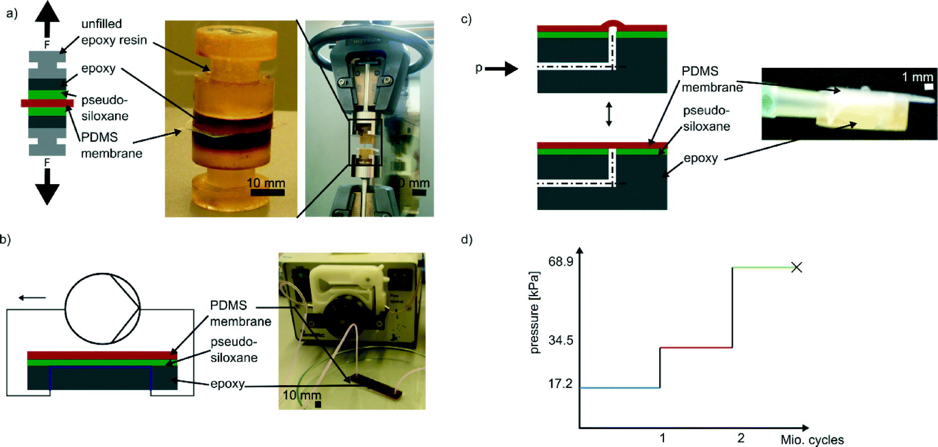 | ||
| Fig. 1 Methods of bond strength testing. a) As depicted in the schematic each sample for tensile testing consisted of two test specimens. The bottom of each test specimen was fabricated from the STL epoxy resin to be tested. Two of these test specimens were treated with the respective surface modification techniques and bonded to the same PDMS membrane. The resulting stack is depicted in the photograph on the left. These samples were then tested with an INSTRON universal testing machine. The photograph on the right shows the tensile testing machine with mounted test specimens. In b) a schematic of the hydrolytic stability testing setup is shown. For this setup a peristaltic pump was connected to a microfluidic chip made of the epoxy to be tested. The open channel of the chip was closed by bonding a flat PDMS slab to the channel using the respective bonding technique. For hydrolytic stability testing dyed water was pumped through the chip until leakage was observed. c) Schematic of the setup for cyclic load testing. Each sample tested consisted of a microfluidic channel made from the respective epoxy resin bonded and sealed with a PDMS membrane using the respective bonding technique. The channel was then connected to a pressurized air-line. With a manually controllable manometer the pressure was set to a specific value. The pressure was then applied and released from the channel at a frequency of 10 Hz using computer controllable valves. Applying pressure to the channel results in bulging of the membrane as required, e.g., for microfluidic valves or pumps. d) Load profile applied to each test specimen during cyclic load testing. For the first interval, a pressure of 17.2 kPa was applied for one million cycles. For the second interval, the pressure was doubled to 34.5 kPa and another one million cycles were performed. For the third interval, the pressure was again doubled to 68.95 kPa for another one million load cycles and so forth, until membrane ruptured. | ||
The specimens for these tests were produced in a similar fashion to the ones for tensile testing. A rectangular PDMS mold was used to create a thin layer of the specific cured STL epoxy resin, namely Accura 60 and Watershed XC 11122, before filling the mold completely with epoxy resin 1122A. After demolding the two-layer component was split into five smaller pieces using a saw. Two holes (diameter: 1 mm) were drilled into each of the fragments forming a channel structure with a 90°-turn (see Fig. 1c). The hole was then sealed from the top (i.e., the surface which consisted of the respective STL epoxy resin) with a flexible PDMS membrane using the respective bonding method. The channel was then connected to a pressurised air-line and the pressure set to 17.2 kPa via a manually controllable manometer. Using a computer controllable valve (type Angar scientific 2312, Angar scientific inc., USA) this pressure was applied cyclically to the sample at a frequency of 10 Hz. After every 30 hours (which corresponds to about one million load cycles) the pressure was doubled to 34.5 kPa. This pressure was reported as effective pressure for pneumatically controlled push-down valves made by soft lithography.30 After another 30 hours the pressure was doubled again resulting in a step-wise increasing load profile (see Fig. 1d). The next step, 68.9 kPa, was chosen because this pressure is used in pressure driven flow focusing.31 During the whole time the membranes were checked for delamination, rupture or sealing failures.
Hydrolytic stability testing
In lab-on-a-chip applications particularly in biology or biochemistry, water is the most commonly encountered liquid. As a matter of fact, the bond as well as all materials that form the channel walls is exposed to every fluid flowing through the channel. If the chemistry used for creating the bond is not stable against these fluids this would obviously result in bond failure after an unpredictable period of time. To ensure that a bonding technique is applicable to microfluidic systems, the hydrolytic stability of the bonds created with the specific technique has to be assessed. For a sol–gel process similar to the technique used in our experiments this has been done by Suzuki et al.32 who fabricated a hybrid microdevice from PMMA and PDMS using TEOS. However, for the two newly introduced photoinduced surface modification techniques presented in this work, hydrolytic stability has to be investigated.In order to do so microfluidic chips containing one channel (width: 250 μm, height: 250 μm, length: 45 mm) manufactured from Accura 60, Watershed XC 11122 and DSM 12120 HT, respectively, were manufactured using STL by Proform AG (Switzerland).
These channels were bonded to a PDMS membrane using either the GPTMS or DMDMS photoinduced bonding method. The samples were connected to a peristaltic pump (type MC-MS/CA-4/8, purchased from Ismatec, Germany) using polytetrafluoroethylene (PTFE) tubes (see Fig. 1b). The samples were then probed with water. The flow rate within the microfluidic channel was 170 μl min−1. During the whole experiment the samples were examined for leakage.
Results and discussion
Determining the best bonding technique for an epoxy resin
As discussed, the surface properties of stereolithographically structured epoxy resins vary widely. Therefore, it is necessary to determine the best bonding technique for the respective epoxy resin. One limiting criterion is the glass transition temperature of the epoxy to be bonded. If this temperature is 60 °C or lower a photoinduced bonding method has to be chosen. Exposing low glass transition temperature epoxy resins to heat during a sol–gel curing process may result in permanent deformation or damage of the microstructures and therefore has to be avoided. The next question to ask is which silane couples best to the specific epoxy surface. In theory the coupling behaviour is dependent on the predominant functional groups on the surface to be bonded.A simple method for investigating the effectiveness of surface modifications is based on measurement of the advancing surface contact angle. This method is often used in literature in order to determine whether a specific silane was successfully coupled to a surface. Table 1 summarizes the results of water contact angle measurements carried out on cured Accura 60, Watershed XC 11122 and DSM 12120 HT surfaces. The uncoated cured epoxy surface shows contact angles of around 70° for water. After creation of the siloxane layer a significant increase in the advancing contact angle can be observed on all epoxy surfaces, indicating that the surface has been modified successfully.
| Investigated epoxy material | Pure epoxy surface | Epoxy modified with GPTMS using UV light | Epoxy modified with DMDMS using UV light | Epoxy modified with DMDMS using sol–gel method |
|---|---|---|---|---|
| a Purely absorbed siloxane layer which proved to be unusable for bonding. | ||||
| Accura 60 | 71.5° ± 3.25° | 84.6° ± 1.85° | 103.4°a ± 3.17° | 81.8°a ± 0.92° |
| Watershed XC 11122 | 66.2° ± 1.46° | 96.06 ± 0.78a | 90.01° ± 12.28° | 77.97° ± 3.52° |
| DSM 12120 HT | 70.2° ± 2.73° | 87.5°a ± 2.28° | 106.0° ± 5.34° | 82.3° ± 2.58° |
However, successful creation of a siloxane layer is only the first step of the bonding process. We found contact angle measurement not sufficient to predict whether or not the surface was suitable for creating bonds of sufficient strengths. This is due to the fact that the creation of the siloxane layer may have been in fact successful but the linkage of this layer to the surface has been insufficient. The explanation for this behaviour is a result of the ability of the silane to crosslink, even if it is unable to couple to the surface chemically. This results in a purely adsorbed siloxane layer created on top of the respective cured epoxy surface. Depending on the silane used this adsorbed siloxane layer may have the same surface properties as covalently correctly coupled siloxane layers and therefore shows identical contact angles (see Table 1). We therefore characterized all substrates using pull-off tests. During these test we found that siloxane layers made from DMDMS are not able to efficiently link to Accura 60. On the other hand siloxane layers created from GPTMS are not effectively linked to Watershed XC 11122 and DSM 12120 HT. From the last two materials the membranes could be peeled off easily by hand. As depicted in Table 1 these combinations showed the same shift in the contact angle as the ones that could be used for efficient bonds.
The contact angles of the pure surfaces also cannot be used to predict the silane which should be used for bonding. As depicted in Table 1 Accura 60 and DSM 12120 HT exploit almost the same contact angle even though the silanes that form sufficient bonds on these surfaces are not the same. This result could be substantiated by contact angle measurements with solvents of different polarities on uncoated epoxy components for which the experimental data can be found in the ESI.†
Characterization of bondable surfaces
For all bondable surfaces more precise characterization of the surface chemistry was carried out using XPS. Table 2 shows the atomic concentration of coated epoxy samples. These are compared to the atomic concentration of the pure epoxy polymer, which also was determined using XPS. Table 2 indicates a significant rise in the silane concentration due to the surface modification. At the same time the count of carbon atoms diminished. This indicates that the siloxane has effectively been applied to the surface. However, comparing the scans of the pure epoxy components, we were unable to identify a significant difference which allows a prediction about the best silane to use in order to create efficient bonds. The same applies for the ATR-IR spectra, which can be found in the ESI.† Thus carrying out simple pull-off tests is the easiest way to determine the best-suited silane for each resin.| Sample | C | O | F | Si | Cl |
|---|---|---|---|---|---|
| Watershed XC 11122 pure | 80.6 | 18.7 | 0.4 | 0.3 | |
| Watershed XC 11122 + DMDMS UV | 48.5 | 25.6 | 25.9 | ||
| Watershed XC 11122 + DMDMS sol gel | 49.9 | 25.7 | 24.4 | ||
| DSM 12120 HT pure | 71.7 | 22.90 | 5.4 | ||
| DSM 12120 HT +DMDMS UV | 49.9 | 26.8 | 23.3 | ||
| DSM 12120 HT + DMDMS sol gel | 49.6 | 27.3 | 23.1 | ||
| Accura 60 pure | 73.6 | 24.3 | 2.1 | ||
| Accura 60 + GPTMS UV | 56.4 | 32.0 | 0.4 | 11.2 |
Narrow XPS scans of O 1s, C 1s, Si 2p, and valence band of uncoated and coated epoxy samples were compared with the literature reference for PDMS.33Fig. 2 exemplarily depicts the Narrow XPS scans of DSM 12120 HT. It can be seen that the coated surfaces are almost identical to the reference spectrum whereas the pure epoxy sample shows significant variances in all four scans.
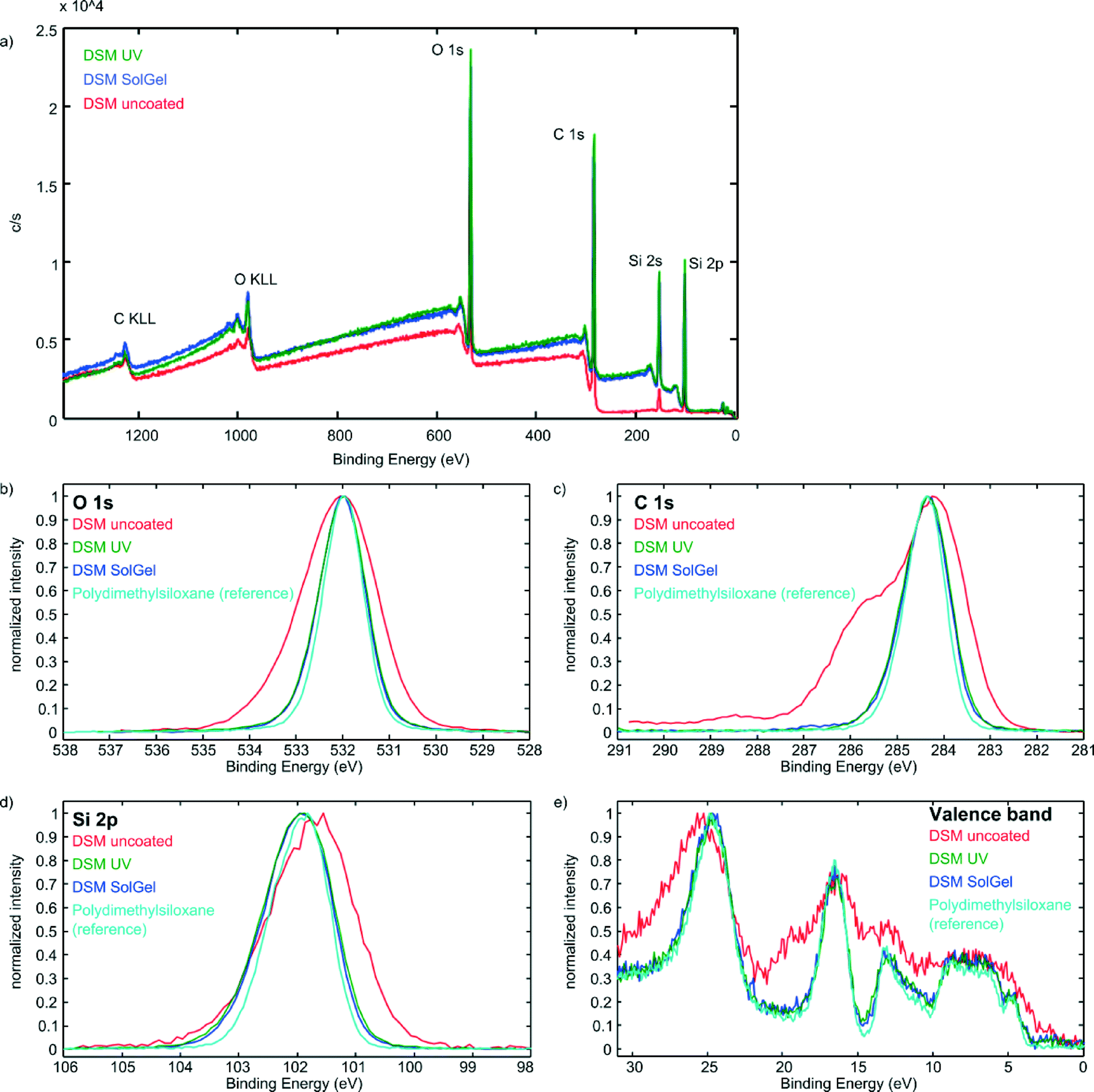 | ||
| Fig. 2 Survey (a) and narrow XPS scans of O 1s (b), C 1s (c), Si 2p (d), and valence band (e) of pure and coated DSM 12120 HT samples. As depicted the spectra of the coated samples are almost identical with the spectrum of pure PDMS which has been taken from the literature.33 The curves of pure DSM 12120 HT, which were obtained using the same method show significant differences compared to the PDMS reference. The spectra of the other epoxy materials and their coated surfaces can be found in the ESI.† These measurements show that the created layers resemble PDMS very closely chemically. | ||
The structure of uncoated and coated surfaces was investigated using SEM. The images obtained from Accura 60 surfaces are depicted in Fig. 3 (pictures of Watershed XC 11122 and Somos DSM 12120 HT can be found in the ESI†). The pure sample (Fig. 3a) shows the typical striped structure of a stereolithographically structured substrates. This structure is generated during the manufacturing process when the polymer is polymerized layer by layer with a typical layer thickness of 50–100 μm to form the component. The reasons for the large standard deviation we see in the results of the contact angle measurement results from this microstructure. Even after surface modification the structure can be clearly seen on the SEM images. In addition to the striped structure the coated samples also exploit a sporadic unevenness which is due to the formation of polysiloxane agglomerated during the coating process (see Fig. 3c). The lateral dimensions of these agglomerates vary between 3 μm and 35 μm.
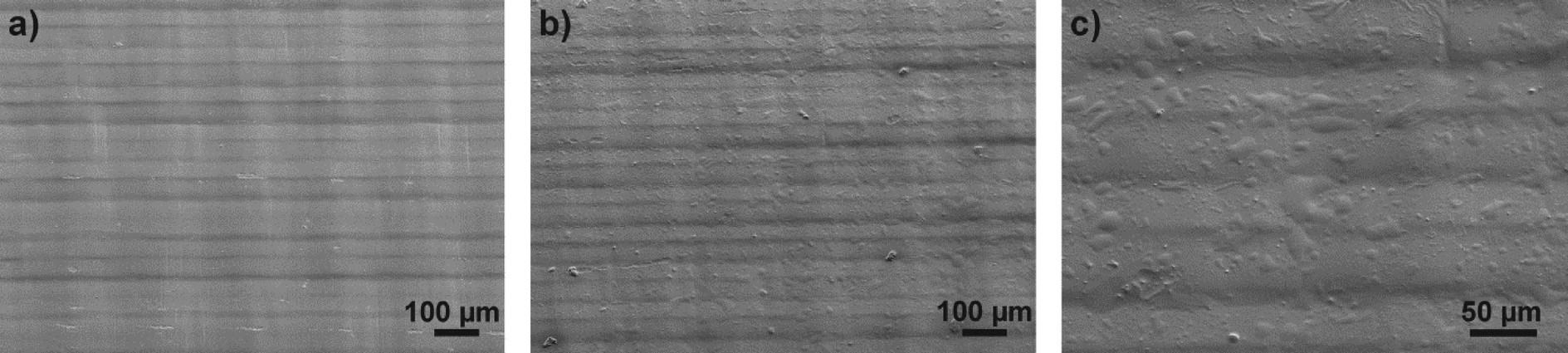 | ||
| Fig. 3 SEM images of Accura 60 surfaces before and after coating. a) The image of a pure Accura 60 surface shows the stripped structure that is commonly found on all stereolithographically structured components. The lines indicate the individual layers that have been polymerized one after another during the manufacturing process. b) This structure can also be seen on the coated device. c) A close up at the coated surface shows that the coating introduces an additional unevenness. This might be due to the fact that the surplus silane agglomerates on the surface. Similar results have been obtained for the other materials. The pictures of these experiments can be found in the ESI.† | ||
Maximum bond strength determined in DIN EN-conform tensile testing
To determine this bond strength we carried out tensile tests on at least five samples for each silane/epoxy-pair that did form a sufficient bond in preliminary experiments. The resulting average bond strengths, the standard deviations as well as the maximum and minimum bond strengths are summarized in Table 3. In literature values of average bond strengths of 300 kPa for plasma-induced PDMS/PDMS bonds and 290 kPa for corona-induced PDMS/PDMS bonds have been reported.28| Epoxy resin | Accura 60 | Somos DSM 12120 HT | Watershed XC 11122 | ||
|---|---|---|---|---|---|
| Silane + bonding method | GPTMS + UV | DMDMS + UV | DMDMS + sol–gel | DMDMS + UV | DMDMS + sol–gel |
| Average bond strength [kPa] | 356.9 ± 211.0 | 67.2 ± 38.8 | 156.8 ± 104.8 | 33.7 ± 19.7 | 193.1 ± 110.5 |
| Maximum bond strength [kPa] | 686.5 | 132.3 | 310.4 | 69.3 | 349.3 |
| Minimum bond strength [kPa] | 156.8 | 30.2 | 77.4 | 15.5 | 54.9 |
However, these values have not been determined using the same test setup. Thus they cannot be directly compared. Our setup eliminates the influence of shear forces completely whereas the setup used in the reference referred to a mixed loading case.28 For information about the behaviour of the respective bonds in mixed load cases see section “Long-term stability of bonded PDMS/epoxy compounds under cyclic loading”.
We found average bond strength of ~360 kPa for Accura 60 samples bonded using a siloxane layer created from GPTMS. This value is higher than reported for pure PDMS/PDMS bonds. It is important to note that without creation of the siloxane layer Accura 60 cannot be bonded to PDMS at all. The bonds on siloxane layer created from DMDMS via the sol–gel-method on DSM 12120 HT and Watershed XC 11122 reached average bond strengths of ~160 kPa and ~210 kPa, respectively. Again, without the siloxane layer bonding of these substrates is not possible at all. Using the photoinduced siloxane layer from DMDMS we obtained bond strengths of ~70 kPa and ~30 kPa for DSM 12120 HT and Watershed XC 11122, respectively. In general, bonds on siloxane layers created from DMDMS via the photoinduced technique were not as strong as the bonds that were formed on the same epoxy substrate using the sol–gel process. However for most STL epoxies the photoinduced bonding is preferable, because it is a mild process that requires no solvent or heat treatment. As discussed, deformation or permanent damage may result from these treatments, especially given the fact that the sol–gel process requires a mixture of water, ethanol and hydrochloric acid. If strongly crosslinked epoxy resins with high glass transition temperatures are used, the sol–gel process is a good alternative for creating stronger bonds. The big variance between the maximum and minimum values that can be seen for all sample types has been reported to be a typical phenomenon for plasma- and corona-induced bonding methods.28 As the actual bonding between the siloxane layer and the PDMS substrates was based on corona activation we expected comparable variations in bond strengths.
Long-term stability of bonded PDMS/epoxy compounds under cyclic loading
In membrane actuators the bond between the membrane and the chip material is always exposed to shear forces. The effect of these forces cannot be simulated with tensile testing. In order to determine the suitability of bonding techniques for creation of bonds that will sustain long-term shear force loading, e.g., in a membrane actuator, we performed cyclic load tests in a membrane actuator setup. Two samples made of Accura 60 bonded with GPTMS via UV-light and two samples of Watershed XC 11122 bonded with DMDMS using the sol–gel process were tested. All of them endured more than one million cycles of pressurised air at 17.2 kPa and 10 Hz which amounts to a total duration 30 hours. The load was then increased to 34.5 kPa and the samples were again exposed cyclically for one million cycles at the same frequency for another 30 hours. Again all samples tested endured this interval. According to literature this pressure can be used to set up pneumatically controlled push-down valves.30 Thus the bond would be suitable for such applications. The load was then doubled again to 68.9 kPa and loaded cyclically at the same frequency. After 56 minutes (33600 duty cycles) the bond on one sample made of Watershed XC 11122 failed. In total this sample sustained about 2.3 million duty cycles and failed due to membrane rupture, not due to failure of the bond. The second sample to fail was made of Accura 60. This sample endured a total of 2.4 million duty cycles (with 49800 cycles at 68.9 kPa) before it failed, again due to membrane rupture not as a consequence of bond failure. The bond on the second sample of Watershed XC 11122 failed after approximately 3.5 million duty cycles, also due to membrane rupture. The only sample that failed as a consequence of bond failure was the bond on the second sample of Accura 60. At the time of failure this sample had endured about 3.5 million duty cycles.
In summary, all bonding techniques yielded, if applied using the correct silane on the respective epoxy surface, bonds of strength and durability which exceed by far the demands of typical microfluidic applications, such as pneumatically controlled valving or pressure driven flow focusing. They all endured more than two million duty cycles which amounts in a total duration of 60 hours at 10 Hz. Again, it has to be noted that none of the material combinations tested can be bonded without the siloxane layer.
Hydrolytic stability assessment
As discussed, the photoinduced creation of the siloxane layer is a technique which we are first to report. Therefore hydrolytic stability of this bonding technique needs to be assessed. In contrast to tensile testing, there is no accepted standard for this kind of tests. We therefore decided to mimic an application scenario running water, the most important solvent in lab-on-a-chip devices for biochemistry and biology, through a channel made from the respective epoxy resin bonded to a PDMS membrane. For this purpose six microfluidic chips were bonded with the photoinduced technique. Two of these chips were made from Accura 60 (bonded with GPTMS via UV-light), two consisted of DSM 12120 HT (bonded with DMDMS via UV light) and the other two were fabricated from Watershed XC 11122 (bonded with DMDMS via UV light). After approximately three hours one of the chips made from Watershed XC 11122 broke due to a bond failure. The failure of the sample may be due to a manufacturing defect in the bond. The second sample to fail was an Accura 60 sample, which failed after approximately 292 hours. Before the sample failed the membrane that covered the channel inlet was bulged to an enormous extend. This indicates that the channel was blocked by a small particle. Since the volume controlled pump did not halt the pressure underneath the membrane grew continuously. At a certain point the bond was no longer able to resist this pressure. All other chips endured the hydrolytic stability testing for more than 840 hours, which is about five weeks, before the experiment was stopped. Thus both bonding techniques may be regarded as hydrolytically stable.Conclusions
In summary, we showed three easy to use surface modification techniques that allow bonding of a wide range of commercially available STL epoxy resins using siloxane layers as intermediate bonding layers. The need for more than one technique arises from different material properties of various STL resins. Using GPTMS we were able to bond Accura 60 to PDMS. As second technique we propose creating the siloxane layer using DMDMS by sol–gel chemistry. This was done on Watershed XC11122 and DSM 12120 HT. For both silanes we demonstrated photoinduced creation of the siloxane layer resulting in a sufficiently strong bond between the siloxane and the epoxy surface. This photoinduced modification requires neither solvent nor heat which avoids deformation or swelling of the bulk material. Even though this technique is preferable for most epoxy resins we also showed that creation of the siloxane layer made of DMDMS using a sol–gel process leads to higher overall bond strengths. However, due to the necessity of using organic solvents and heat treatments this technique is limited to high temperature epoxy resins. The photoinduced technique as well as the sol–gel based technique creates siloxane layers which lend themselves well to corona-activated bonding to PDMS, which is a commonly used method for bonding PDMS to PDMS. Using one of the reported methods for creating the siloxane layer allows the creation of bondable surfaces on nearly every commercially available epoxy surface. The complete bonding process, including the preceding surface modification, can be carried out within half an hour with both of the photoinduced techniques. The sol–gel modification is more time-consuming as the gelation process takes about two hours. As bonding itself relies on corona-based surface activation, the procedure can be carried out in every lab. Neither clean room conditions nor special vacuum chambers are required.Using DIN EN-conform tensile testing we could proof bond strengths of ~357 kPa for bonds on photoinduced created siloxane layers from GPTMS on Accura 60, ~67 kPa for bonds on photoinduced created siloxane layers from DMDMS on DSM 12120 HT and ~193 kPa for bonds on siloxane layers created on Watershed XC 11122 using DMDMS via the sol–gel technique, respectively. These values compare well with literature values of 290 kPa reported for PDMS/PDMS bonds and outperform these values significantly for some material combinations.28 The best bonding techniques for the respective epoxy surface were subjected to cyclic load testing in order to assess their applicability for membrane actuators. During tests each sample endured at least 2.3 million duty cycles. All but one sample failed due to membrane rupture and not due to bond failure, even at elevated pressures. This indicates that the weak point in these experiments was not the bond but the 300 μm thick PDMS membranes that were used. For the newly reported creation of siloxane layers via photoinduced surface modification methods we also demonstrated hydrolytic stability. In these experiments all but two bonds were leak-tight for more than 840 hours in operation.
In summary, the techniques presented in this paper enable fast and easy bonding STL epoxy components to PDMS. By conducting various characterizing experiments, including DIN EN-conform tensile testing, we could show that the bonds on siloxane layers created with either the described photoinduced or sol–gel based techniques can be used in membrane actuators with millions of load cycles sustained at elevated pressures as well as in microfluidic chips where they are exposed to aqueous solutions.
Acknowledgements
We thank Paul Abaffy for making the SEM images.This work has partly been funded by the German Federal Ministry of Education and Research (BMBF), research grant 16SV5775.
Notes and references
- K. W. Oh and C. H. Ahn, J. Micromech. Microeng., 2006, 16, R13–R39 CrossRef.
- D. J. Laser and J. G. Santiago, J. Micromech. Microeng., 2004, 14, R35–R64 CrossRef.
- T. Thorsen, S. J. Maerkl and S. R. Quake, Science, 2002, 298, 580–584 CrossRef CAS PubMed.
- E. Wilhelm, C. Neumann, K. Sachsenheimer, T. Schmitt, K. Länge and B. E. Rapp, Lab Chip, 2013, 13, 2268–2271 RSC.
- A. Waldbaur, H. Rapp, K. Länge and B. E. Rapp, Anal. Methods, 2011, 3, 2681–2716 RSC.
- A. Waldbaur, B. Carneiro, P. Hettich, E. Wilhelm and B. Rapp, Microfluid. Nanofluid., 2013, 15, 625–635 CrossRef.
- J.-W. Choi, H.-C. Kim and R. Wicker, J. Mater. Process. Technol., 2011, 211, 318–328 CrossRef CAS PubMed.
- C.-W. Tsao and D. L. DeVoe, Microfluid. Nanofluid., 2009, 6, 1–16 CrossRef CAS.
- J. K. Lee, K.-W. Park, J. C. Choi, H.-R. Kim and S. H. Kong, J. Micromech. Microeng., 2012, 22, 115028 CrossRef.
- D. Cai and A. Neyer, Microfluid. Nanofluid., 2010, 9, 855–864 CrossRef CAS.
- B. H. Jo, L. M. Van Lerberghe, K. M. Motsegood and D. J. Beebe, J. Microelectromech. Syst., 2000, 9, 76–81 CrossRef CAS.
- K. Haubert, T. Drier and D. Beebe, Lab Chip, 2006, 6, 1548–1549 RSC.
- N. Y. Lee and B. H. Chung, Langmuir, 2009, 25, 3861–3866 CrossRef CAS.
- Z. Zhang, P. Zhao and G. Xiao, Polymer, 2009, 50, 5358–5361 CrossRef CAS PubMed.
- L. Tang and N. Y. Lee, Lab Chip, 2010, 10, 1274–1280 RSC.
- B. Cortese, M. C. Mowlem and H. Morgan, Sens. Actuators, B, 2011, 160, 1473–1480 CrossRef CAS PubMed.
- N. Y. Lee and B. H. Chung, Langmuir, 2009, 25, 3861–3866 CrossRef CAS.
- M. E. Vlachopoulou, A. Tserepi, P. Pavli, P. Argitis, M. Sanopoulou and K. Misiakos, J. Micromech. Microeng., 2009, 19, 015007 CrossRef.
- K. Kim, S. W. Park and S. S. Yang, BioChip J., 2010, 4, 148–154 CrossRef CAS.
- K. S. Lee and R. J. Ram, Lab Chip, 2009, 9, 1618–1624 RSC.
- V. Sunkara, D.-K. Park, H. Hwang, R. Chantiwas, S. A. Soper and Y.-K. Cho, Lab Chip, 2011, 11, 962–965 RSC.
- K. Aran, L. A. Sasso, N. Kamdar and J. D. Zahn, Lab Chip, 2010, 10, 548–552 RSC.
- N. Du, J. Chou, E. Kulla, P. N. Floriano, N. Christodoulides and J. T. McDevitt, Biosens. Bioelectron., 2011, 28, 251–256 CrossRef CAS PubMed.
- V. Sunkara, D.-K. Park and Y.-K. Cho, RSC Adv., 2012, 2, 9066–9070 RSC.
- E. T. Vandenberg, L. Bertilsson, B. Liedberg, K. Uvdal, R. Erlandsson, H. Elwing and I. Lundström, J. Colloid Interface Sci., 1991, 147, 103–118 CrossRef CAS.
- Y. H. Tennico, M. T. Koesdjojo, S. Kondo, D. T. Mandrell and V. T. Remcho, Sens. Actuators, B, 2010, 143, 799–804 CrossRef CAS PubMed.
- J. Wu and N. Y. Lee, Lab Chip, 2014, 14, 1564–1571 RSC.
- M. A. Eddings, M. A. Johnson and B. K. Gale, J. Micromech. Microeng., 2008, 18, 067001 CrossRef.
- B. E. Rapp, L. Carneiro, K. Länge and M. Rapp, Lab Chip, 2009, 9, 354–356 RSC.
- V. Studer, G. Hang, A. Pandolfi, M. Ortiz, W. F. Anderson and S. R. Quake, J. Appl. Phys., 2004, 95, 393–398 CrossRef CAS PubMed.
- T. Ward, M. Faivre, M. Abkarian and H. A. Stone, Electrophoresis, 2005, 26, 3716–3724 CrossRef CAS PubMed.
- Y. Suzuki, M. Yamada and M. Seki, Sens. Actuators, B, 2010, 148, 323–329 CrossRef CAS PubMed.
- The XPS of polymers database, ed. G. Beamson and D. Briggs, SurfaceSpectra Ltd., Manchester, UK, 2000 Search PubMed.
Footnote |
| † Electronic supplementary information (ESI) available: Additional XPS measurements, ATR-IR spectra, SEM images of coated and uncoated surfaces and contact angle measurements of solvents with different polarities on uncoated epoxies. See DOI: 10.1039/c4lc01440e |
| This journal is © The Royal Society of Chemistry 2015 |