
 Open Access Article
 This Open Access Article is licensed under a Creative Commons Attribution-Non Commercial 3.0 Unported Licence
Direct observation of the energetics at a semiconductor/liquid junction by operando X-ray photoelectron spectroscopy†
Michael F.
Lichterman‡
ab,
Shu
Hu‡
ab,
Matthias H.
Richter‡
b,
Ethan J.
Crumlin‡
c,
Stephanus
Axnanda
c,
Marco
Favaro
bc,
Walter
Drisdell
bc,
Zahid
Hussain
c,
Thomas
Mayer
d,
Bruce S.
Brunschwig
*be,
Nathan S.
Lewis
*abf,
Zhi
Liu
*cgh and
Hans-Joachim
Lewerenz
*b
aDivision of Chemistry and Chemical Engineering, California Institute of Technology, Pasadena, CA 91125, USA
bJoint Center for Artificial Photosynthesis, California Institute of Technology, Pasadena, CA 91125, USA. E-mail: bsb@caltech.edu; nslewis@caltech.edu; lewerenz@caltech.edu
cAdvanced Light Source, Lawrence Berkeley National Laboratory, Berkeley, CA 94720, USA. E-mail: zliu2@lbl.gov
dSurface Science Division, Materials Science Department, Darmstadt University of Technology, 64287 Darmstadt, Germany
eBeckman Institute, California Institute of Technology, Pasadena, CA 91125, USA
fKavli Nanoscience Institute, California Institute of Technology, Pasadena, CA 91125, USA
gState Key Laboratory of Functional Materials for Informatics, Shanghai Institute of Microsystem and Information Technology, Chinese Academy of Sciences, Shanghai 200050, People's Republic of China
hSchool of Physical Science and Technology, ShanghaiTech University, Shanghai 200031, China
First published on 29th May 2015
Abstract
Photoelectrochemical (PEC) cells based on semiconductor/liquid interfaces provide a method of converting solar energy to electricity or fuels. Currently, the understanding of semiconductor/liquid interfaces is inferred from experiments and models. Operando ambient-pressure X-ray photoelectron spectroscopy (AP-XPS) has been used herein to directly characterize the semiconductor/liquid junction at room temperature under real-time electrochemical control. X-ray synchrotron radiation in conjunction with AP-XPS has enabled simultaneous monitoring of the solid surface, the solid/electrolyte interface, and the bulk electrolyte of a PEC cell as a function of the applied potential, U. The observed shifts in binding energy with respect to the applied potential have directly revealed ohmic and rectifying junction behavior on metallized and semiconducting samples, respectively. Additionally, the non-linear response of the core level binding energies to changes in the applied electrode potential has revealed the influence of defect-derived electronic states on the Galvani potential across the complete cell.
Broader contextWhile much work has been devoted to the study of semiconductor/liquid junctions, the direct observation by XPS methods of the semiconductor/liquid junction under applied biases has not heretofore been explored. We demonstrate that the operando XPS technique applied to a semiconductor/liquid junction can directly measure the positions of the electronic states of the electrode and the electrolyte. The use of tender X-rays allows for the direct evaluation of the energetics for the electrode surface, the electrochemical double layer, and the adjacent bulk water. The data provide direct insight into the nature of the rectifying or ohmic junction in addition to allowing for the calculation of defect state densities and band bending in such photoelectrochemical half cells. All of these directly observed parameters are crucial variables for the design and operation of semiconductor–liquid junction devices. |
Introduction
Electrochemical-solar energy conversion is based on the rectifying properties of semiconductor–electrolyte junctions. The fundamental concept of semiconductor/electrolyte contacts was introduced by Gerischer in 1975.1 The theory was based on the relation of the Fermi energy EF of a solid to the electrochemical potential of an electrolyte.2 Gerischer drew an analogy between semiconductor/liquid contacts and a Schottky contact at semiconductor/metal interfaces.3–5 At equilibrium the Fermi energy EF of the semiconductor must equal −e![[small mu, Greek, macron]](https://www.rsc.org/images/entities/i_char_e0cd.gif) Se where Se is the electrochemical potential of the electron in solution and e is the absolute charge of an electron. This causes equilibration charge to flow between the semiconductor and the solution and produces a space-charge region in the semiconductor with an accompanying electric field. The electric field causes the energy of the electron levels to “bend” as they move through the field and shifts the relative positions of the Fermi energy and the solution electrochemical potential. At the semiconductor/liquid junction, only a small fraction of the overall contact potential difference drops across the electrochemical double layer in solution.1,6,7 The electrochemical potential of a phase is given by = μ − eφ, where μ is the chemical potential of the phase and φ is the electrostatic potential of the phase.
Se where Se is the electrochemical potential of the electron in solution and e is the absolute charge of an electron. This causes equilibration charge to flow between the semiconductor and the solution and produces a space-charge region in the semiconductor with an accompanying electric field. The electric field causes the energy of the electron levels to “bend” as they move through the field and shifts the relative positions of the Fermi energy and the solution electrochemical potential. At the semiconductor/liquid junction, only a small fraction of the overall contact potential difference drops across the electrochemical double layer in solution.1,6,7 The electrochemical potential of a phase is given by = μ − eφ, where μ is the chemical potential of the phase and φ is the electrostatic potential of the phase.
The band bending present in the semiconductor space-charge region drives the separation of electron–hole pairs and thus facilitates applications of these systems for photelectrochemical energy conversion. Accordingly, efficient and moderately stable photoelectrochemical energy-conversion systems were developed a few years after the introduction of the concepts outlined above.8,9 Despite many investigations using surface science methods,10–13 however, direct measurements of the energetic relations at a semiconductor/electrolyte junction have not previously been obtained.
In this work, we present a method that allows, in an unprecedented manner, a direct analysis of the electronic properties of a semiconductor/electrolyte junction by applying photoelectron spectroscopy (PES) to semiconductor/electrolyte junctions under near-ambient-pressure conditions. Investigations using ex situ X-ray photoelectron spectroscopy (XPS),14 photocurrent15 and capacitance–voltage spectroscopy,16 spectral response,17 open-circuit photovoltage,18 Fermi-level pinning,19 system design,20 flat-band potential,21 physicochemical principles,22 and various surface-modification strategies23–25 have been performed to characterize the behavior of various semiconductor/liquid junctions. These methods, however, do not allow for the direct observation of the band energetics and surface chemistry that are of fundamental importance to the performance of such systems. Conventional XPS experiments typically are performed under ultra-high vacuum (UHV), and so cannot probe the behavior of the semiconductor/liquid interface under the electrochemical potential control associated with an operating PEC cell. For example, frozen electrolytes in UHV12 have been used to investigate a semiconductor/electrolyte junction and the chemistry therein, but potential control is not possible in such a configuration. The operando experiment allows for the measurement of the kinetic energy of photoelectrons that are emitted from semiconductors in contact with thin water/electrolyte films. The tender X-ray range of 1.5 to 8 keV allows for a range of sampling depths. The use of 4 keV X-rays allows for monitoring each section of thin-layer structures because the inelastic mean-free path, which depends on the photoelectron kinetic energy, is substantially larger than in soft X-ray PES.
X-ray photoelectron spectroscopy can determine the chemical composition and positions of the electronic states (energy-band relations) of a material. X-ray radiation incident on the sample creates photoelectrons with a kinetic energy EK that depends on the binding energy EB of the core level, the photon energy hν, and the work function ϕ of the material. Due to the low inelastic mean-free path (IMFP) of photoelectrons in solids, XPS is surface-sensitive and typically has an information depth in the nanometer range.26 Photoelectrons that are ejected by tender X-rays at 4 keV have IMFPs in the range of 4 to 10 nm (see Table S1, ESI†). The core level emission binding energy reflects a base binding energy E0B and a band-bending term ΔEBB.27 The binding energy of the electrode is given by (see Fig. 1):
| EB,electrode = hν − EK = E0B,electrode + ΔEBB,electrode. | (1) |
| EB,electrolyte(Ueff(U)) = hν − EK − eUeff(U) = E0B,electrolyte + ΔEBB,electrolyte − eUeff(U). | (2) |
Se.| eUeff(U) = eU + E0REF − eSe. | (3) |
 | ||
| Fig. 1 (a) Scheme of the principal arrangement of p+-Si/TiO2/H2O(liq.)/H2O(gas) to the analyzer front cone. (b) The energy band relations of the p+-Si/TiO2/H2O(liq.)/H2O(gas) system under applied potential U. The working electrode (Si) and analyzer are grounded and all the kinetic energies of the emitted photoelectrons are referenced to the Fermi energy of the analyzer. In the three-electrode configuration the Fermi energy is shifted by U with respect to the reference electrode. (c) The core level emission under applied potential (dashed curves) with respect to the core level emission under open circuit (solid line). The effective potential Ueff is given by eUeff(U) = eU + E0REF − Se. | ||
Ambient-pressure X-ray photoelectron spectroscopy (AP-XPS)29–31 has been used to investigate gas/solid and gas/liquid interfaces such as metal oxide formation,32 mechanisms of heterogeneous catalysis,33 oxygen reduction on fuel cell cathodes,34 and other systems.35,36 Recent developments in AP-XPS allow for the use of liquid electrolytes at the surface of interest during operation, therefore closely approximating a conventional PEC cell.37 We demonstrate herein the use of AP-XPS with real-time control of the electrochemical potential through a conductive liquid electrolyte on a PEC system to investigate the chemical and electrochemical nature of a semiconductor/liquid junction.
A three-electrode photoelectrochemical cell using an ∼13 nm thick meniscus thin-film electrolyte on the working electrode permitted electrochemical control (Fig. S2, ESI†) of the solid/liquid interface. XPS analysis was performed at 20–27 mbar by using a differential pumping system in conjunction with a photoelectron analyzer as described elsewhere.37 The resulting operando AP-XPS data were used to directly characterize the behavior of TiO2/electrolyte and TiO2/Ni/electrolyte interfaces that have recently been shown to enhance the stability of small band-gap photoanodes during solar-driven water oxidation to produce O2(g).38 The AP-XPS data have allowed experimental confirmation of key theoretical aspects of the behavior of semiconductor/liquid junctions, directly revealing the band energetics and interfacial electronic structures of such systems.
Experimental
Films of amorphous TiO2 produced by atomic-layer deposition (ALD)38 were prepared on degenerately boron-doped p-type silicon (“p+-Si”) substrates (see ESI† for details). The silicon provided a topologically flat, ohmic back contact and did not otherwise contribute to the results described herein. An ALD cycle consisted of a 0.1 s pulse of tetrakis(dimethylamido)titanium (TDMAT) followed by a 15 s purge of N2 at 20 sccm, followed by a 0.015 s pulse of water before another 15 s N2 purge. For Ni-containing electrodes, Ni was deposited by RF sputtering for 20 s to 60 s with a sputtering power of 150 W.Operando AP-XPS data were collected using a differentially pumped Scienta R4000 HiPP-2 system that allowed a pressure of 20–27 mbar inside the experimental chamber on beamline 9.3.1 at the Advanced Light Source, which was used to provide tender X-rays at 4 keV.37 The pressure range used herein was bounded by an upper limit of photoelectron collection efficiency and detector/analyzer protection and by a lower limit given by the boiling point of water. The p+-Si/TiO2/(Ni) working electrode was grounded to the detector to equalize the Fermi energy of the detector with the back contact of the working electrode. Along with the working electrode, the Ag/AgCl reference and platinum foil counter electrodes were mounted and contacted to a three-axis manipulator (Fig. S2, ESI†). The electrodes were ‘dipped and pulled’ into an electrolyte-filled beaker (1.0 M KOH) and were positioned in front of the XPS sampling cone while maintaining contact with the electrolyte. The XPS collection position was optimized to maximize signal detection for both the electrode and electrolyte, as previously reported in investigations of the solution/metal interface37 and as described further in the ESI.† Although the data were obtained in a hanging meniscus “emersion” configuration, negligible steady-state faradaic current was passed at any potential in the experiments described herein. Hence, the working electrode was under potential control and comprised an isopotential surface, so the experimental method is appropriately designated as operando. The data were analyzed with CasaXPS and IgorPro. 1.0 M KOH(aq) provided a conductive and adhering thin-film electrolyte that enabled AP-XPS data to be collected while maintaining potential control of the electrode. In conjunction with AP-XPS data, current density vs. potential (J–U) data (Fig. S3, ESI†) were collected on p+-Si/TiO2 and p+-Si/TiO2/Ni working electrodes in a conventional three-electrode potentiostatic configuration. Electrochemical J–U and impedance vs. potential data were recorded on SP-200 and SP-300 Bio-Logic potentiostats. The impedance data were fitted with a Randles equivalent circuit using EC-LAB software to extract the differential capacitance (Cd) vs. potential data of the interface.
Results
Fig. 2 depicts the O 1s core level spectra for a p+-Si/TiO2 electrode, in 0.2 V steps, for potentials between −1.4 V and +0.4 V vs. Ag/AgCl. The data show the shift in O 1s binding energies as a function of the electrode potential, U, for the oxygen in H2O(g), H2O(l), OH− and TiO2, respectively. Ti 2p core level spectra are also shown at these same electrode potentials. Analogous data were also obtained for TiO2-coated electrodes that additionally contained a film of Ni/NiOx on the surface (Fig. S4, ESI†). Fig. 3 shows the change in peak position vs. potential for the O 1s and Ti 2p data for (a) a bare p+-Si/TiO2 electrode and (b) a p+-Si/TiO2/Ni electrode. Fig. 4 and Fig. S5 (ESI†) summarize the band-edge positions and band-bending information on the semiconductor/liquid interface obtained from the data of Fig. 3a. | ||
| Fig. 2 Raw AP-XPS data and fitted peaks for the O 1s and Ti 2p peaks at potentials between +0.4 V and −1.4 V vs. Ag/AgCl for a bare p+-Si/TiO2 electrode. Peaks for H2O gas, H2O liquid, OH−, O 1s (TiO2), and Ti 2p are shown; the center of each peak position for the liquid water, O 1s (TiO2), and Ti 2p peaks at each potential has been marked with a black line. | ||
 | ||
| Fig. 3 (a) AP-XPS peak positions of O 1s and Ti 2p3/2 signals for liquid water and TiO2 as a function of the potential, U, of a bare p+-Si/TiO2 electrode in 1.0 M KOH(aq). Different potential regions U1 to U4 are shown. A solid line corresponding to a slope of Δ = −1 eV V−1 has been drawn through the water O 1s data; a solid line drawn as a visual guide is shown for the titania data. (b) Analogous AP-XPS peak positions vs. electrode potential for a p+-Si/TiO2/Ni (deposited by 60 s of Ni sputtering) electrode. | ||
 | ||
| Fig. 4 Schematic energy diagram of the TiO2/liquid junction. (a) For highly negative bias (U1 region, red lines), band shifting in the TiO2 is observed (<−1.2 V). (b) In the ideal semiconductor region U2, from −0.9 V to −0.6 V (blue lines), band bending in the TiO2 is observed (compare to Fig. 3) with no further potential drop in the electrochemical double layer. (c) For increased positive biased (U3 region, green lines), the Fermi level is pinned to the defect states, and the TiO2 bands shift with the complete potential drop that occurs in the electrochemical double layer. (d) At potentials positive of −0.2 V (region U4), ideal behavior is once again observed. In all cases, the shift in water O 1s binding energy is linear with the applied voltage. The Ti 2p binding energy shifts linearly for band bending regimes (U2 and U4) and remains constant for the band shifting regimes (U1 and U3). | ||
In addition to Mott–Schottky (Cd−2 − U) data, Fig. 5 depicts the full width at half maximum (FWHM), as well as the higher and lower binding-energy half widths at half maximum (HWHM+, HWHM−), for the Ti 2p3/2 peak of a p+-Si/TiO2 electrode. The potential at which the minimum peak width was observed (i.e. the expected flat-band potential) in the AP-XPS data, Ufb = −0.9 V vs. Ag/AgCl, was in excellent agreement with the flat-band potential extracted from the conventional, electrochemically based, Mott–Schottky analysis (Fig. 5b).
 | ||
| Fig. 5 (a) High and low energy half widths at half maximum (HWHM+, HWHM−) for the Ti 2p3/2 peak of a p+-Si/TiO2 electrode as a function of applied potential. The higher binding energy half width, HWHM+, is shown in blue and the lower binding energy half width, HWHM−, in red. The inset depicts the overall full width at half maximum (FWHM = HWHM+ + HWHM−) as a function of applied potential. The blue, red, and black lines are guide-lines for the eye. Error bars are ∼±0.1 eV for the half widths; while the error bars are considerably larger than the trends at negative potentials, the data confirms that the width of the peak increases with an absolute value of U as expected from theoretical simulation. (b) Mott–Schottky data for a p+-Si/TiO2 electrode, with Ufb calculated as −0.9 V vs. Ag/AgCl from a linear fit; a Randles circuit was used as the equivalent circuit. | ||
Discussion
Semiconductor/liquid junctions resemble semiconductor/metal (Schottky) junctions.39 It is well accepted, but has not been directly shown, that an ideal semiconductor/liquid junction has band edges that are essentially fixed with respect to the electrochemical potential of contacting electrolytes when a Galvanic potential is applied between the semiconductor working electrode and a reference electrode in a three-electrode cell. Ideally, the band edges are fixed at semiconductor/liquid interfaces, and the Galvani potential drops across the space-charge region in the semiconductor, giving rise to “band bending”. Hence, the rectifying behavior of semiconductor/liquid junctions shares the same “band bending” origin as those in Schottky junctions, and semiconductor/liquid junctions have accordingly been exploited for photoelectrochemical solar-energy conversion and storage.40 In the presence of surface or bulk electronic states that have energies in the band gap of the semiconductor, the Galvani potential should drop partially (or completely, depending on the density of the surface states) across the surface, partially (or completely) at bulk in-gap states, and/or across the semiconductor space-charge region. The partial (or complete) filling of defect states results in Fermi level pinning19 at the occupation limit of the surface defects, and thus pinning of semiconductor band edges should in principle be observable using AP-XPS. Upon application of a potential to a semiconductor/liquid junction, several “band bending” conditions can thus be established: flat-band, accumulation, depletion with or without Fermi level pinning, and strong inversion at increased positive potentials (for an n-type semiconductor). Except for the latter, all of these “band bending” conditions have been directly observed, characterized, and analyzed by operando AP-XPS in this work.For a metal/liquid contact, the metal core level binding energies remain constant with respect to various applied potentials, i.e. flat-band conditions are maintained because metals cannot support electric fields in their bulk, and thus have a constant potential within the metal. Therefore, for metal/liquid interfaces, the Galvani potential drops across the electrolyte double layer (the Helmholtz layer). In contrast, the potential drop across the double layer is negligible for an ideal semiconductor/liquid junction. Such flat-band conditions may also be observed with a metallized semiconductor surface that acts as a metal, wherein an ohmic electrical connection is established between the semiconductor and metal.
Although the aforementioned theory is generally accepted and used to design PEC devices,25,41 the PEC-AP-XPS experiments described herein have allowed a direct verification of the theoretically expected behavior for the semiconductor/liquid junctions under evaluation. The semiconductor core level peaks in an ideal semiconductor/liquid junction should exhibit the same decrease in measured binding energies (notated EB, with units of electron volts) with applied potential (UApplied) as the liquid water O 1s peaks, with a slope of Δ = −1 eV V−1. This behavior is expected if the band bending occurs exclusively in the semiconductor electrode; the electron analyzer and working electrode are grounded at the same Fermi level and the binding energies of the core levels are always referenced to this equalized Fermi level (Fig. S2, ESI†). In contrast, for a metal/liquid junction, the metal core levels are expected to maintain a constant binding energy with varying applied potentials, where the potential difference drops across the electrochemical double layer (ECDL). In both cases, the bulk liquid water (i.e. water outside the double layer) core levels should shift consistently with the applied potential because the electrochemical potential of bulk liquid water is constant with respect to the reference electrode.
As shown in Fig. 3a, on the p+-Si/TiO2 electrode, the liquid water O 1s peak shifted linearly with the applied potential, with a slope of Δ = −1 eV V−1. This slope is expected when the contribution to the binding energy shift is negligible from water within the electrochemical double layer. This condition is applicable to the conditions investigated herein, because the width of the double layer is ∼1 nm in 1.0 M KOH(aq). The inelastic mean-free path (IMFP) for the O 1s electrons in water is ∼10 nm at EK = 3466 eV (the average kinetic energy of the water O 1s photoelectron from an X-ray photon energy of 4 keV).42 Therefore, for an ∼13 nm thick electrolyte film, the double layer is expected to make only a small contribution to the overall peak position. Extra-atomic relaxation or surface charging can be neglected as well (see ESI† for details).
In contrast to the behavior of the O 1s H2O signal, the observed TiO2 O 1s and Ti 2p core level binding energies were not a monotonic function of the applied potential, U. For the TiO2 electrode, the Ti 2p and TiO2 O 1s peak binding energies did not shift linearly with potential over the entire potential range (Fig. 3a). At potentials, U, between −1.4 V and −1.0 V vs. Ag/AgCl (notated as U1) and −0.6 V and −0.2 V vs. Ag/AgCl (notated as U3), the binding energies of the Ti 2p and O 1s (TiO2) core levels stayed nearly constant. Fig. S6 (ESI†) shows a second set of data for a different set of samples, demonstrating the reproducibility of the relative peak shifts with respect to the applied potential U.
As illustrated in Fig. 4a, in region U1 the Fermi level potential is shifted negative of the conduction band edge position. This behavior results in the formation of an accumulation layer in which semiconductor surface conduction-band states are being filled with electrons, resulting in a high surface concentration of electrons. Therefore, further band bending downwards is inhibited, and the Fermi level is “pinned” at the position of the TiO2 conduction band minimum. For U < −1 V vs. Ag/AgCl, the accumulation layer causes a shift of the band edges with the applied potential in the same fashion as that expected for a metal/liquid junction. Instead of a potential drop due to band bending in TiO2, under such conditions, the potential drops across the double layer. Given that the conduction-band edge is located close to −1.0 V vs. Ag/AgCl, the constant binding energies observed for U < −1.0 V vs. Ag/AgCl are in excellent agreement with the Mott–Schottky analysis as well as with prior electrochemical data for n-TiO2 photoelectrodes.43
The core level binding energy was also not sensitive to the applied potential in the range −0.6 to −0.2 V (U3) (see Fig. 4). This potential range is located energetically between the conduction band and the middle of the band gap. This insensitivity to applied potential is attributed to charging and discharging of TiO2 defect states and is explained by Fermi level pinning.19 As illustrated in Fig. 4c, when the applied voltage places the Fermi energy across the defect state region, the charging and discharging of the defect states lead to the voltage dropping at the defect states and double layer instead of producing additional band bending in the semiconductor. As shown in ex situ XPS data depicted in Fig. S7 (ESI†), these defect states exist at energies 1.8–2.8 eV above the top of the TiO2 valence band. This energetic location corresponds to a potential range of −0.7 to +0.3 V vs. Ag/AgCl, which spans the energy range within which the binding energy insensitivity was observed by operando AP-XPS. The observed behavior is thus in excellent agreement with separate, prior photoelectrochemical and photoelectron spectroscopy measurements.10,44 Beyond a sufficiently positive applied voltage, 0 V vs. Ag/AgCl, the defect states are sufficiently discharged to allow for a return to nearly ideal semiconductor/liquid junction behavior, as shown in Fig. 4d.
Sputter deposition of Ni makes the TiO2 films anodically conductive, such that the TiO2/Ni combination may be used for photoanode protection.38 As shown in Fig. 3b and Fig. S4 (ESI†), the addition of Ni substantially altered the potential response observed in the AP-XPS data. Specifically, the binding energies of the TiO2 core levels became almost independent with respect to the electrolyte, i.e. the Fermi level of the TiO2 was pinned by the Ni layer. Ni will quickly react under oxidizing conditions to form a nickel oxide but, once formed, NiOx is stable under our operating conditions, per the Pourbaix diagram for Ni. As indicated by Fig. 3b, the addition of Ni allows for the ALD-TiO2 to maintain a band structure much closer to flat-band across the entire potential range examined herein, thus removing a large voltage barrier to conduction. Effectively, the electrical connection between the surface of the Ni-deposited TiO2 and the solution converts the electrical behavior of the solid/liquid junction from rectifying to ohmic. This behavior appeared to be generally true across the TiO2/Ni electrode, as evidenced by the uniform coverage of Ni on the electrode (Fig. S8, ESI†), as opposed to a mechanism involving localized islands or pinholes leading to charge conduction. These observations are relevant to elucidating the anodic conduction mechanism observed previously in amorphous TiO2/Ni films and the importance of the Ni contact. The addition of Ni removes a rectifying barrier from the TiO2/solution interface which would otherwise block charge conduction.38 As was shown for the p+-Si/TiO2 electrodes, these results were similarly reproduced (Fig. S6) (ESI†).
One measure with which to prove the validity of the AP-XPS approach is to derive electrochemical parameters directly from the XPS data and then to compare these values to independent measurements of the same quantities. When substantial band bending is present, the XPS sampling depth will collect photoelectrons across a range of binding energies. Hence, for a semiconductor capable of supporting a space-charge region, a broader XPS peak is expected for potentials at which band bending is maximized, and a narrower XPS peak should be observed for potentials close to flat-band conditions (see ESI† for details). Therefore, the flat-band potential (Ufb) of the semiconductor can be obtained solely from operando AP-XPS measurements, without the use of Mott–Schottky45 analysis. Based on this approach, the flat-band potential observed by AP-XPS coincides with the minimum of the FWHM and HWHM data. The Mott–Schottky data yielded Ufb = −0.9 V vs. Ag/AgCl, agreeing well with other investigations for n-type TiO2.43 The FWHM and HWHM data from the AP-XPS analysis exhibited a minimum near −0.9 V vs. Ag/AgCl (Fig. 5), demonstrating that semiconductor electrochemistry data can be derived directly from operando AP-XPS data, without the need for an equivalent-circuit based model, which is required to analyze the interfacial impedance data. The HWHM and FWHM data accurately describe this system as defined by Mott–Schottky analysis, and demonstrate the internal consistency between the different parts of the data reported herein. As shown in Fig. S9 (ESI†), for a metallized system that effectively appears ohmic, no clear dependence was observed between the Ti 2p3/2 FWHM and the applied voltage. A further description of the analysis of these data is contained in the ESI.†
In conjunction with a model based on metal-oxide-semiconductor (MOS) solar cells,46,47 the AP-XPS allows for the derivation of an equation that quantifies the density of electrochemically active defect states in a semiconductor/liquid junction. In the mid-gap potential region, where a deviation from the ideal core level binding energy shift for TiO2 of Δ = −1 eV V−1 was observed, defect states are associated with the voltage drop that is not observed across the semiconductor. Hence, the lack of change in the binding energies of the core levels of the semiconductor, relative to the expected 1![[thin space (1/6-em)]](https://www.rsc.org/images/entities/char_2009.gif) :1 shift in binding energy with the applied voltage, can be used to measure the defect-state density by eqn (4):
:1 shift in binding energy with the applied voltage, can be used to measure the defect-state density by eqn (4):
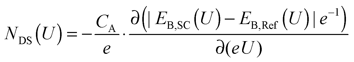 | (4) |
Conclusions
The operando photoelectron spectroscopic investigation of a photoelectrochemical cell has been demonstrated and applied to describe the operational characteristics of important semiconductor/liquid junctions. Tender X-ray analysis enables the investigation of the semiconductor surface, the electrolyte double layer and the bulk water layer, while maintaining electrochemical control over the entire system. Moreover, the potential range over which data could be collected extended beyond the thermodynamic limits for the oxidation or reduction of water. Semiconductor accumulation, depletion and Fermi level pinning by defect states were directly quantified by tender X-ray AP-XPS, in addition to ohmic and/or rectifying behavior depending on the behavior of metallized semiconductor/film contacts. Further use of the tender AP-XPS method will enable a detailed, direct understanding of the behavior of other important semiconductors, metals, and composite semiconductor–electrocatalyst systems for water photolysis and (light-induced) carbon dioxide reduction.Author contributions
MFL, SH and MHR contributed to the design, execution, and analysis of the experiment; EJC was critical in the design, building and testing of the endstation that allows atmospheric pressure XPS data collection on a solution under potentiostatic control. SA contributed to design of the end station; MF and WD contributed to data collection; ZH provided direction and funding for the end station; TM, BSB, NSL, ZL, and H-JL advised on the undertaking and analysis of the experiment.Acknowledgements
This work was supported through the Office of Science of the U.S. Department of Energy (DOE) under award no. DE-SC0004993 to the Joint Center for Artificial Photosynthesis, a DOE Energy Innovation Hub. The Advanced Light Source is supported by the Director, Office of Science, Office of Basic Energy Sciences, of the U.S. Department of Energy under Contract no. DE-AC02-05CH11231. We acknowledge Dr. Philip Ross for his contributions to the conceptual development of the AP-XPS endstation and experimental design, and Junko Yano for fruitful discussions. We acknowledge Fadl Saadi, Beomgyun Jeong, and Sana Rani for assistance during data collection at the beamline.References
- H. Gerischer, J. Electroanal. Chem. Interfacial Electrochem., 1975, 58, 263–274 CrossRef CAS
.
-
S. R. Morrison, Electrochemistry at Semiconductor and Oxidized Metal Electrodes, New York, 1st edn, 1980 Search PubMed
- W. Schottky, Z. Phys., 1939, 113, 367–414 CrossRef CAS
- W. Schottky, Phys. Z., 1940, 41, 570–573 Search PubMed
- W. Schottky, Z. Phys., 1942, 118, 539–592 CrossRef CAS
- H. Gerischer, Z. Phys. Chem., 1960, 26, 223–247 CrossRef CAS
- H. Gerischer, Z. Phys. Chem., 1961, 27, 48–79 CrossRef CAS
- A. Heller, Acc. Chem. Res., 1981, 14, 154–162 CrossRef CAS
- A. Heller, Catal. Rev., 1984, 26, 655–681 Search PubMed
- K. Schwanitz, E. Mankel, R. Hunger, T. Mayer and W. Jaegermann, Chimia, 2007, 61, 796–800 CrossRef CAS
- M. Sander, W. Jaegermann and H. J. Lewerenz, J. Phys. Chem., 1992, 96, 782–790 CrossRef CAS
- T. Mayer, M. V. Lebedev, R. Hunger and W. Jaegermann, J. Phys. Chem. B, 2006, 110, 2293–2301 CrossRef CAS PubMed
- T. Mayer, M. Lebedev, R. Hunger and W. Jaegermann, Appl. Surf. Sci., 2005, 252, 31–42 CrossRef CAS PubMed
- J. C. Bernède, S. Houari, D. Nguyen, P. Y. Jouan, A. Khelil, A. Mokrani, L. Cattin and P. Predeep, Phys. Status Solidi A, 2012, 209, 1291–1297 CrossRef PubMed
- A. Heller, K. C. Chang and B. Miller, J. Am. Chem. Soc., 1978, 100, 684–688 CrossRef CAS
- K. Kobayashi, Y. Aikawa and M. Sukigara, J. Appl. Phys., 1983, 54, 2526–2532 CrossRef CAS PubMed
- A. Heller, K. C. Chang and B. Miller, J. Electrochem. Soc., 1977, 124, 697–700 CrossRef CAS PubMed
- N. S. Lewis, J. Electrochem. Soc., 1984, 131, 2496–2503 CrossRef CAS PubMed
- A. J. Bard, A. B. Bocarsly, F. R. F. Fan, E. G. Walton and M. S. Wrighton, J. Am. Chem. Soc., 1980, 102, 3671–3677 CrossRef CAS
- A. J. Bard, J. Phys. Chem., 1982, 86, 172–177 CrossRef CAS
- P. Allongue and H. Cachet, Solid State Commun., 1985, 55, 49–53 CrossRef CAS
- A. J. Nozik and R. Memming, J. Phys. Chem., 1996, 100, 13061–13078 CrossRef CAS
- B. Miller, A. Heller, S. Menezes and H. J. Lewerenz, Faraday Discuss. Chem. Soc., 1980, 70, 223–232 RSC
- J. R. C. Lattimer, B. S. Brunschwig, N. S. Lewis and H. B. Gray, J. Phys. Chem. C, 2013, 117, 27012–27022 CAS
- M. G. Walter, E. L. Warren, J. R. McKone, S. W. Boettcher, Q. Mi, E. A. Santori and N. S. Lewis, Chem. Rev., 2010, 110, 6446–6473 CrossRef CAS PubMed
- M. P. Seah and W. A. Dench, Surf. Interface Anal., 1979, 1, 2–11 CrossRef CAS PubMed
-
J. F. Moulder, W. F. Stickle, P. E. Sobol and K. D. Bomben, Handbook of X-ray Photoelectron Spectroscopy, 1995 Search PubMed
- S. Trasatti, Pure Appl. Chem., 1986, 58, 955–966 CAS
- M. Salmeron and R. Schlögl, Surf. Sci. Rep., 2008, 63, 169–199 CrossRef CAS PubMed
- D. E. Starr, Z. Liu, M. Hävecker, A. Knop-Gericke and H. Bluhm, Chem. Soc. Rev., 2013, 42, 5833–5857 RSC
- E. J. Crumlin, H. Bluhm and Z. Liu, J. Electron Spectrosc. Relat. Phenom., 2013, 190, 84–92 CrossRef CAS PubMed
- A. Y. Klyushin, T. C. R. Rocha, M. Hävecker, A. Knop-Gericke and R. Schlögl, Phys. Chem. Chem. Phys., 2014, 16, 7881–7886 RSC
- V. V. Kaichev, I. P. Prosvirin and V. I. Bukhtiyarov, J. Struct. Chem., 2012, 52, 90–101 CrossRef
- H. S. Casalongue, S. Kaya, V. Viswanathan, D. J. Miller, D. Friebel, H. A. Hansen, J. K. Nørskov, A. Nilsson and H. Ogasawara, Nat. Commun., 2013, 4, 2817 Search PubMed
- D. Zemlyanov, B. Aszalos-Kiss, E. Kleimenov, D. Teschner, S. Zafeiratos, M. Hävecker, A. Knop-Gericke, R. Schlögl, H. Gabasch, W. Unterberger, K. Hayek and B. Klötzer, Surf. Sci., 2006, 600, 983–994 CrossRef CAS PubMed
- Y.-C. Lu, E. J. Crumlin, G. M. Veith, J. R. Harding, E. Mutoro, L. Baggetto, N. J. Dudney, Z. Liu and Y. Shao-Horn, Sci. Rep., 2012, 2, 715 Search PubMed
- S. Axnanda, E. J. Crumlin, B. Mao, S. Rani, R. Chang, P. G. Karlsson, M. O. M. Edwards, M. Lundqvist, R. Moberg, P. Ross, Z. Hussain and Z. Liu, Sci. Rep., 2015, 5, 9788 CrossRef PubMed
- S. Hu, M. R. Shaner, J. A. Beardslee, M. F. Lichterman, B. S. Brunschwig and N. S. Lewis, Science, 2014, 344, 1005–1009 CrossRef CAS PubMed
- J. Tersoff, Phys. Rev. Lett., 1984, 52, 465–468 CrossRef CAS
- P. V. Kamat, K. Tvrdy, D. R. Baker and J. G. Radich, Chem. Rev., 2010, 110, 6664–6688 CrossRef CAS PubMed
-
M. X. Tan, P. E. Laibinis, S. T. Nguyen, J. M. Kesselman, C. E. Stanton and N. S. Lewis, Principles and Applications of Semiconductor Photoelectrochemistry, John Wiley & Sons, Inc., Hoboken, NJ, USA, 1994, vol. 41 Search PubMed
- D. Emfietzoglou and H. Nikjoo, Radiat. Res., 2007, 167, 110–120 CrossRef CAS PubMed
- M. Radecka, M. Rekas, A. Trenczek-Zajac and K. Zakrzewska, J. Power Sources, 2008, 181, 46–55 CrossRef CAS PubMed
- K. Schwanitz, U. Weiler, R. Hunger, A. Thomas Mayer and W. Jaegermann, J. Phys. Chem. C, 2006, 111, 849–854 CrossRef
- F. Fabregat-Santiago, G. Garcia-Belmonte, J. Bisquert, P. Bogdanoff and A. Zaban, J. Electrochem. Soc., 2003, 150, E293–E298 CrossRef CAS PubMed
- H. Kobayashi, T. Mori, K. Namba and Y. Nakato, Solid State Commun., 1994, 92, 249–254 CrossRef CAS
- H. Kobayashi, Y. Yamashita, T. Mori, Y. Nakato, T. Komeda and Y. Nishioka, Jpn. J. Appl. Phys., 1995, 34, 959–964 CrossRef CAS
Footnotes |
| † Electronic supplementary information (ESI) available. See DOI: 10.1039/c5ee01014d |
| ‡ These authors contributed equally to the work. |
| This journal is © The Royal Society of Chemistry 2015 |