High efficiency hybrid PEDOT:PSS/nanostructured silicon Schottky junction solar cells by doping-free rear contact†
Yunfang
Zhang
ab,
Wei
Cui
a,
Yawen
Zhu
a,
Fengshuo
Zu
a,
Liangsheng
Liao
a,
Shuit-Tong
Lee
a and
Baoquan
Sun
*a
aInstitute of Functional Nano & Soft Materials (FUNSOM), Soochow University, 199 Ren'ai Road, Suzhou, 215123, Jiangsu, People's Republic of China. E-mail: bqsun@suda.edu.cn
bDepartment of Mathematics and Physics, Jiangsu University of Science and Technology, Zhenjiang, 212003, People's Republic of China
First published on 21st October 2014
Abstract
A high doping technique has been widely used for record-efficiency crystalline silicon (Si) solar cells to minimize the series resistance losses and to form a back surface field. However, it requires high temperatures (up to 1000 °C) and involves toxic gases, which may not be compatible for hybrid organic–silicon solar cells. Here, we report that a high power conversion efficiency (PCE) of 13.7% with a device area of 0.8 cm2 has been achieved for organic-nanostructured Si hybrid solar cells by inserting a cesium carbonate (Cs2CO3) layer between Si and the rear electrode aluminium (Al), which is realized by a solution process under low-temperature annealing (<150 °C). Transient and constant current–voltage, capacitance–voltage, and scanning Kelvin probe microscope measurements are used to characterize the effect of the Cs2CO3 layer on the device performance. The insertion of Cs2CO3 not only decreased the contact resistance, but also generated a built-in electric field on the rear electrode. The recombination rates are suppressed at the back surface due to the deflection of minority carriers. These findings show a promising strategy to achieve high performance organic–silicon solar cells with a simple, low temperature and cost effective process.
Broader contextOrganic–inorganic hybrid photovoltaic devices exhibit significant potential as they offer a simple and low temperature fabrication process, which can combine the advantages of both organics and inorganics for low cost and high efficiency photovoltaics (PVs). The exploration of novel interfacial materials with the required charge selectivity and compatibility is critical for hybrid PVs, and a proper combination of the interfacial layer with the active layer is the key to improve the power conversion efficiency (PCE). Here, we report that nanostructured silicon–organic hybrid PVs with a PCE of up to 13.7% under air mass 1.5G irradiation was achieved through interfacial engineering of a solution-processed cesium carbonate layer. The cesium carbonate layer was inserted between silicon and aluminum without any high temperature doping process (<150 °C), which resulted in facilitating electron extraction and suppressing charge recombination. These results offer an important concept for achieving high performance organic–silicon photovoltaic devices with a simple, low temperature, and cost-effective process. In addition, this concept can be also used for improving the metal–semiconductor contact. |
Introduction
Transparent conducting polymer–silicon (Si) hybrid Schottky solar cells have attracted wide research interest due to their simple device structure compared with the Si-based traditional p–n junction photovoltaics.1–10 One of the most important advantages of organic–Si hybrid solar cells is that they allow the stacking of different materials without the strict requirements of lattice matching in Si heterojunctions. Poly(3,4-ethylenedioxythiophene)/poly(styrenesulfonate) (PEDOT:PSS) has been extensively investigated for hybrid solar cells due to its high transparency and conductivity.9,11–13 Various approaches have been made to enhance the performance of this kind of the device, such as Si surface passivation,10,14–16 surface morphology controlling,3,9,11,13,17–19 and property tuning of PEDOT:PSS.4,7,20–22 A power conversion efficiency (PCE) of over 13% has been achieved for the PEDOT:PSS/Si solar cells.8,23,24 In addition, carbon nanotubes (CNTS)–Si heterojunction photovoltaics with efficiencies of up to 15% by coating a TiO2 antireflection layer and doping CNTs with oxidative chemicals as a transparent window have been demonstrated.25 However, to the best of our knowledge, there has hardly been any investigation on the rear electrode, which plays a critical role in device performance.2,3 Generally, the cathode is either Ga:In eutectic, aluminum (Al) or Ti/Pd/Ag.8,10,11 The physical mechanism of the rear electrode has not been a popular topic of research for the hybrid solar cells.2,3,18Traditionally, the Si–metal ohmic contact is synthesized by high p- or n-doping at high temperatures (up to 1000 °C)26 to form the back surface field. This process requires the use of hazardous doping gases, such as diborane (B2H6) and phosphine (PH3), which poses operational and environmental issues. Moreover, doping has a detrimental effect on the quality of crystalline Si, because it results in the creation of additional Si dangling bonds. Furthermore, due to the high temperatures required and the complicated process, the doping method may be not compatible for organic–Si hybrid solar cells.
Cesium carbonate (Cs2CO3) has been used as an effective electron-injection (and hole-blocking) layer at the cathode interface in organic devices.27,28 This is mainly ascribed to the decreased work function (WF) of Cs2CO3/Al due to Cs2CO3 decomposing into cesium oxide (Cs2O) when annealed.29 In addition, an Al–O–Cs structure is formed while thermally evaporating Al, which further lowers the WF of Al.28 A solution fabrication process can be used to avoid any physical and chemical stresses at the interface, thus leading to better junction properties.30
Here, we develop an alternative back contact method by inserting a Cs2CO3 layer between the rear side of n-Si and Al for a Si/PEDOT:PSS solar cell. Nanostructured Si is used to increase the light harvesting capability. When the Cs2CO3 layer is inserted between nanostructured Si and the rear electrode Al, a high PCE of 13.7% is achieved, which is a 27% improvement in comparison to a Si/Al direct contact device (PCE: 10.8%).
Experimental section
Preparation of nanostructured Si
The nanostructured Si was prepared by a metal ion-assisted electroless chemical etching process.31 Planar Si substrates (n-type Si (100)) with a resistivity of 0.05–0.1 Ω cm were immersed in a solution of hydrofluoric acid (HF) (4.8 M) and silver nitride (AgNO3) (0.02 M) at room temperature for 5 min. Then, they were rinsed with deionized water and dipped in a nitric acid (HNO3) solution. To reduce the surface/volume ratio, the substrates were immersed in a solution of HF (4.8 M) for 10 min and anisotropic tetramethyl ammonium hydroxide (TMAH)/DI water (v/v = 1![[thin space (1/6-em)]](https://www.rsc.org/images/entities/char_2009.gif) :
:![[thin space (1/6-em)]](https://www.rsc.org/images/entities/char_2009.gif) 25) for 30 s.
25) for 30 s.
Device fabrication
Cs2CO3 and polyethylenimine (PEI) were dissolved in 2-methoxyethanol with a concentration of 0.5 mg mL−1 and 1 mg mL−1, respectively. A Cs2CO3/PEI (v/v = 1![[thin space (1/6-em)]](https://www.rsc.org/images/entities/char_2009.gif) :
:![[thin space (1/6-em)]](https://www.rsc.org/images/entities/char_2009.gif) 1) mixture solution was spin coated onto the rear of nanostructured Si substrates, and then annealed with infrared radiation for 20 min. A highly conductive PEDOT:PSS (CLEVIOS PH 1000) solution mixed with 5 wt% dimethyl sulfoxide (DMSO) and 1 wt% Triton (from Aldrich) was spin-coated onto the front side of the nanostructured Si substrates. Then, the substrates were annealed at 125 °C for 30 min in a nitrogen atmosphere. A silver grid electrode was deposited on top of the PEDOT:PSS layer through a shadow mask. A 150 nm-thick Al film was deposited onto the rear Si substrates by thermal evaporation (Mini-SPECTROS, Kurt J. Lesker Co.). The active area of the device was 1 cm × 0.8 cm.
1) mixture solution was spin coated onto the rear of nanostructured Si substrates, and then annealed with infrared radiation for 20 min. A highly conductive PEDOT:PSS (CLEVIOS PH 1000) solution mixed with 5 wt% dimethyl sulfoxide (DMSO) and 1 wt% Triton (from Aldrich) was spin-coated onto the front side of the nanostructured Si substrates. Then, the substrates were annealed at 125 °C for 30 min in a nitrogen atmosphere. A silver grid electrode was deposited on top of the PEDOT:PSS layer through a shadow mask. A 150 nm-thick Al film was deposited onto the rear Si substrates by thermal evaporation (Mini-SPECTROS, Kurt J. Lesker Co.). The active area of the device was 1 cm × 0.8 cm.
Device characterization
The photovoltaic characterization was conducted under ambient conditions. A Newport 91160 solar simulator equipped with a 300 W xenon lamp and an air mass (AM) 1.5 filter were used to generate a simulated solar spectrum irradiation source. The irradiation intensity was 100 mW cm−2, which was calibrated with a Newport Si solar cell 91150. A Newport monochromator 74125 and power meter 1918 with a Si detector 918D were used in the external quantum efficiency (EQE) measurements. All of the electrical data were recorded by a Keithley 2612 source meter. The capacitance versus voltage (C–V) measurements were carried out with a Wayne Kerr 6500B impedance analyzer. The reflection spectrum was measured by a spectrometer (Perkin-Elmer Lambda 750) with an integrating sphere. Morphology and scanning Kelvin probe microscopy (SKPM) were characterized with an atomic force microscope (AFM, Veeco, Multimode V). The nanostructured Si was characterized with a high-resolution scanning electron microscope (SEM) (Carl Zeiss, Supra 55). Optical microscopy images were obtained from a fluorescence optical microscope (Laica, DM4000M). Regarding the transient electric output characteristic setup, the devices were connected to a digital oscilloscope with an input impedance of 1 MΩ. The intensity of white light, which is referred to henceforth as a “light bias”, was used to control the open-circuit voltage (Voc) of the devices. A laser with a wavelength of 532 nm was used as optical perturbation, pulse duration was set to 1 μs and frequency to 100 Hz, which resulted in a voltage transient with a peak value of 10 mV (≪Voc). The frequency, light intensity and pulse duration were kept constant, with the photocurrent transient at an impedance of 50 Ω.Results and discussion
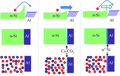
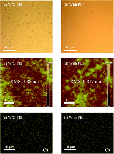
The organic–inorganic hybrid device was generally assumed to be a Schottky junction between n-Si, PEDOT:PSS, and the rear electrode.32 PEDOT:PSS acted as a window electrode, which allowed light to reach Si. The PEDOT:PSS film displayed good light transparency (300–1100 nm, >90%) with a high conductivity (up to 1000 S cm−1).33 In order to improve the hole collection efficiency, a silver grid electrode was deposited onto the PEDOT:PSS film. PEDOT:PSS with a WF of ∼5.1 eV (ref. 33) was used for hole collection and Al as the rear metal for electron collection. Light was harvested by the Si substrate, and a built-in electric field was formed in Si to sweep the charges towards the proper direction. For the rear contact of the most hybrid organic–silicon devices, a metal layer (e.g., Al) is directly deposited on Si,7 as shown in Fig. 1(a). In an ideal metal–semiconductor Schottky barrier, the barrier height is mainly determined by the properties of the metal and the metal–semiconductor interface. For Si, the barrier height was nearly independent of the doping concentration. There was a large energy barrier between Al and Si, and electrons have to pass through this barrier to be collected by Al. In addition, there was an equal amount of electrons and holes at the Si interface, and thus charge recombination became a serious issue. If the rear contact was ohmic, then the electrons could be effectively collected by Al and the total charge recombination could be minimized. A few methods were used to tune the barrier height of the metal and silicon interface.26 Traditionally, a thin highly doped layer (<10 nm) was incorporated, and the effective barrier height for a given metal–semiconductor interface was tuned, as shown in Fig. 1(c). For the contact with a thin n++Si layer, the barrier was dramatically reduced due to the tunneling effect. In addition, an electric field was formed at the rear interface, which suppressed the holes that flow to the rear surface. The hole concentration was thus maintained at higher levels in the bulk of the device, and hence the recombination velocity decreased. Cs2CO3 was inserted between Si and Al in order to decrease the barrier height, as shown in Fig. 1(b). In addition, charge recombination was also suppressed, which was similar to the thin n++Si layer. A device without Cs2CO3 was used as the reference.Pristine Cs2CO3 was unable to form a continuous film on a Si substrate through a spin-coating process. As shown in the optical microscope images in Fig. 2(a), large particles were formed due to Cs2CO3 re-crystallization during the spin-coating process. The film displayed a discontinuous layer (shown in the AFM images in Fig. 2(c)), and therefore uncovered regions still existed where Al could still directly contact with Si. The film quality was dramatically improved when PEI was added to the Cs2CO3 solution, which is shown in Fig. 2(b) and (d). The surface roughness of both the films was characterized by AFM in terms of root-mean-square (RMS) roughness. PEI, which exhibited a high number of amine groups (the chemical structure of PEI is shown in Fig. S1†), displayed excellent dispersion properties in a methoxyethanol solution. The incorporation of PEI formed a uniform film with a RMS value of 0.817 nm, as extracted from the AFM image, while the film based on pristine Cs2CO3 displayed a rather rough surface with a RMS value of 1.88 nm. Moreover, it assured that Cs2CO3 formed a uniform dispersion on the Si substrate, which was confirmed by the energy-dispersive X-ray spectroscopy of cesium, as shown in Fig. 2(e) and (f). There was almost no difference between Fig. 2(e) and (f), which indicated that the dispersion of Cs2CO3 hardly changed after PEI addition. The energy-dispersive X-ray spectroscopy of carbon was also measured and is shown in Fig. S2.† The concentration of carbon increased with PEI addition, which was ascribed to the carbon source of PEI. When Al was deposited on the uniform Cs2CO3 layer, a mild annealing treatment led to the formation of a Cs–O–Al complex.29
The devices were fabricated to explore the effect of the Cs2CO3 interlayer on the rear contact. Compared to planar Si, nanostructured Si displayed a considerably lower light reflectance, which could dramatically improve the light harvesting capability. The reflectance spectra of planar Si and nanostructured Si coated with PEDOT:PSS are shown in Fig. S3,† where nanostructured Si exhibited an average reflection ratio of ∼15%, while the planar one displayed a reflection ratio of 25%. The morphology of the nanostructured Si (Fig. S4†) revealed that antireflection was provided by the graded index of refraction in the nanostructure.
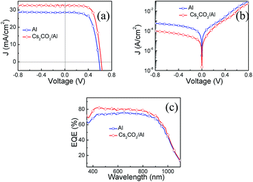
Current versus voltage (J–V) curves of the hybrid solar cells with and without Cs2CO3 under simulated AM 1.5 illuminations at 100 mW cm−2 are shown in Fig. 3(a). The photovoltaic parameters of the short circuit current density (Jsc), the Voc, the fill factor (FF), and the PCE of the hybrid solar cells with and without the Cs2CO3 layer and their statistics (of seven cells for each type) are summarized in Table 1. The excellent device with the Cs2CO3 layer exhibited the highest FF of 68.4%, a Voc of 0.621 V, a Jsc of 32.2 mA cm−2 and a record PCE of 13.7%. The reference device (direct contact of Si and Al) with a Voc of 0.586 V, a Jsc of 28.6 mA cm−2, and a FF of 64.9% yielded a PCE of 10%. The inserted Cs2CO3 layer resulted in 27% PCE enhancement compared with the reference device. The EQE spectra were measured, as shown in Fig. 3(c). The device with the interlayer displayed higher EQE values in the visible and near infrared region when compared with the reference device, which was in line with the enhanced Jsc value.
| Rear electrodea | V oc (V) | J sc (mA cm−2) | FFb (%) | PCEb (%) | R s (Ω cm2) |
|---|---|---|---|---|---|
| a Data and statistics based on seven cells of each condition. b Numbers in bold are the maximum record values. | |||||
| Al | 0.586 0.585(±0.007) | 28.6 28.5(±0.7) | 64.9 63.5 (±1.28) | 10.8 10.5 (±0.3) | 3.46 3.42(±0.3) |
| Cs2CO3/Al | 0.621 0.624(±0.003) | 32.2 31.4 (±0.9) | 68.4 68.8 (±1.14) | 13.7 13.4 (±0.6) | 2.16 2.03(±0.7) |
In order to quantify the improvements in device performance after inserting the Cs2CO3 layer between the nanostructured Si and Al, detailed measurements, including the constant and transient output characteristics and Kelvin scanning microscopy were conducted in the following sections.
Fig. 3(b) shows the J–V characteristics of the hybrid solar cells with and without Cs2CO3 in the dark. It was observed that the saturation current density (Js) was suppressed significantly after the Cs2CO3 layer was inserted between Si and Al. The dark J–V curves were simulated according to the thermionic emission model.34 The Js was obtained by fitting.
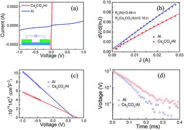
The contact between Al and the rear side of Si was dramatically improved using the Cs2CO3 layer. Al pads were deposited onto Si through thermal evaporation. According to the J–V measurements, as shown in Fig. 4(a), the contact between Si and Al was non-ohmic. A transmission line measurement (TLM) was conducted to measure the contact resistance.35 The detailed TLM method is described in the ESI.† A schematic diagram for measuring the contact resistance value is shown in Fig. S5.† The contact resistance was 3.97 × 10⁻¹ Ω cm2 for the Al/Si direct contact. A non-ohmic contact resulted in a high contact resistance between Si and the rear electrode Al, which led to a charge accumulation at the rear electrode interface. A highly doped layer was used for an improved contact in the traditional Si solar cell, where the contact resistance was reduced to 10−2–10−3 Ω cm2.2,35 The highly doped layer also significantly lowered the saturation current density (to as low as 10−13 A cm−2) and enhanced the Voc.36 Here, with the insertion of the Cs2CO3 layer between Si and Al, the current–voltage curve was linear, as shown in Fig. 4(a), which indicated an improved contact. The contact resistance was 6.18 × 10⁻² Ω cm2 when the Cs2CO3 layer was inserted, which was similar in value to the contact resistance when the high temperature and highly doped process was used. The series resistance (Rs) was extracted from the plot of dV per d (lnJ) versus J (the detailed derivation process is described in the ESI†). Fig. 4(b) shows the dV per day (lnJ) versus J curves of the hybrid solar cell, with and without the Cs2CO3 layer. The device with and without the Cs2CO3 layer displayed Rs values of 2.16 Ω cm2 and 3.46 Ω cm2, respectively, as shown in Table 1. The value of Rs decreased after inserting the Cs2CO3 layer, which was consistent with the improved back contact.
The insertion of the Cs2CO3 layer not only decreased the contact resistance but also generated a larger built-in electric field on the rear electrode. This deflected the minority carriers and recombination rates were suppressed at the back surface. The C−2–V plots at a signal frequency of 1 KHz of the hybrid solar cells with and without Cs2CO3 are shown in Fig. 4(c). C was the capacitance of the device. Here, C−2 was linear with the applied voltage, and the intercept corresponds to the built-in potential. The devices with the Cs2CO3 layer yielded a higher built-in potential than the reference one. A higher built-in potential effectively deflected electrons from migrating towards the cathode.
The improved rear contact and increased built-in potential were ascribed to the Al WF dropping in the presence of the Cs2CO3 layer. The WF change was measured by SKPM under ambient conditions.37,38 Since our devices were characterized in ambient air, the SKPM technique should be suitable to interpret the WF change. The same conductive tip was used during the entire measurement to ensure that its WF remained constant. The relationship between the WF of the conductive tip, Φt, and the samples, Φs is given by
| Φs = Φt − e Vsp |
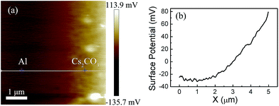 | ||
| Fig. 5 Using SKPM to probe the potential difference of Cs2CO3 and Al. (a) Surface potential images. (b) Cross-section line profile of the surface potential image. | ||
The charge carrier recombination kinetics under open circuit conditions can be explored by transient photovoltaic measurements according to previous reports.39–41 In order to be consistent with the J–V test, the background light intensity was set to 100 mW cm−2. The transient photovoltage (TPV) decay was fitted with a mono-exponential decay equation:
δV = ΔV0![[thin space (1/6-em)]](https://www.rsc.org/images/entities/char_2009.gif) exp(−t/τ) exp(−t/τ) |
Conclusion
In conclusion, we developed a dopant-free rear contact for high performance organic–inorganic polymer/nanostructured Si solar cells. The rear contact was fabricated by inserting a solution processed Cs2CO3 layer between nanostructured Si and Al. An excellent PCE of 13.7% was achieved by this simple and low temperature process (<150 °C). The superior device performance was ascribed to the reduced WF of Al with the Cs2CO3 layer, which resulted in the suppression of the saturation current density, reduced the contact resistance, and enhanced the built-in potential. The improvement of the rear contact allowed the minority carrier to be deflected, leading to the suppression of carrier recombination. This simple, low temperature fabrication process for the hybrid solar cells is promising for low cost photovoltaics.Acknowledgements
This work was supported by the National Basic Research Program of China (973 Program) (2012CB932402), National Natural Science Foundation of China (91123005, 61176057, 61211130358), Jiangsu Key Laboratory for Carbon-Based Functional Materials & Devices, the Priority Academic Program Development of Jiangsu Higher Education Institutions and Collaborative Innovation Center of Suzhou Nano Science and Technology. We would appreciate Mr Tam Jasper for the very detailed paper reading and correction.Notes and references
- M. J. Sailor, E. J. Ginsburg, C. B. Gorman, A. Kumar, R. H. Grubbs and N. S. Lewis, Science, 1990, 249, 1146–1149 CAS.
- Y. Zhang, F. Zu, S. T. Lee, L. Liao, N. Zhao and B. Sun, Adv. Energy Mater., 2014, 4, 1300923 Search PubMed.
- S. Jeong, E. C. Garnett, S. Wang, Z. Yu, S. Fan, M. L. Brongersma, M. D. McGehee and Y. Cui, Nano Lett., 2012, 12, 2971–2976 CrossRef CAS PubMed.
- I. Khatri, Z. Tang, Q. Liu, R. Ishikawa, K. Ueno and H. Shirai, Appl. Phys. Lett., 2013, 102, 063508 CrossRef PubMed.
- S. Avasthi, S. Lee, Y. L. Loo and J. C. Sturm, Adv. Mater., 2011, 23, 5762–5766 CrossRef CAS PubMed.
- S. C. Shiu, J. J. Chao, S. C. Hung, C. L. Yeh and C. F. Lin, Chem. Mater., 2010, 22, 3108–3113 CrossRef CAS.
- J. P. Thomas, L. Y. Zhao, D. McGillivray and K. T. Leung, J. Mater. Chem. A, 2014, 2, 2383–2389 CAS.
- P. Yu, C. Y. Tsai, J. K. Chang, C. C. Lai, P. H. Chen, Y. C. Lai, P. T. Tsai, M. C. Li, H. T. Pan, Y. Y. Huang, C. I. Wu, Y. L. Chueh, S. W. Chen, C. H. Du, S. F. Horng and H. F. Meng, ACS Nano, 2013, 7, 10780–10787 CrossRef CAS PubMed.
- L. He, D. Lai, H. Wang, C. Jiang and Rusli, Small, 2012, 8, 1664–1668 CrossRef CAS PubMed.
- L. He, C. Jiang, H. Wang, D. Lai and Rusli, Appl. Phys. Lett., 2012, 100, 073503 CrossRef PubMed.
- W. R. Wei, M. L. Tsai, S. T. Ho, S. H. Tai, C. R. Ho, S. H. Tsai, C. W. Liu, R. J. Chung and J. H. He, Nano Lett., 2013, 13, 3658–3663 CrossRef CAS PubMed.
- T. G. Chen, B. Y. Huang, H. W. Liu, Y. Y. Huang, H. T. Pan, H. F. Meng and P. Yu, ACS Appl. Mater. Interfaces, 2012, 4, 6857–6864 CAS.
- T. G. Chen, B. Y. Huang, E. C. Chen, P. Yu and H. F. Meng, Appl. Phys. Lett., 2012, 101, 033301 CrossRef PubMed.
- F. Zhang, B. Sun, T. Song, X. Zhu and S. Lee, Chem. Mater., 2011, 23, 2084–2090 CrossRef CAS.
- D. Liu, Y. Zhang, X. Fang, F. Zhang, T. Song and B. Sun, IEEE Electron Device Lett., 2013, 34, 345–347 CrossRef CAS.
- M. Y. Bashouti, M. Pietsch, G. Brönstrup, V. Sivakov, J. Ristein and S. Christiansen, Prog. Photovoltaics, 2013, 22, 1050–1061 Search PubMed.
- H. Jeong, H. Song, Y. Pak, I. K. Kwon, K. Jo, H. Lee and G. Y. Jung, Adv. Mater., 2014, 26, 3445–3450 CrossRef CAS PubMed.
- J. Schmidt, V. Titova and D. Zielke, Appl. Phys. Lett., 2013, 103, 183901 CrossRef PubMed.
- K. Sato, M. Dutta and N. Fukate, Nanoscale, 2014, 6, 6092–6101 RSC.
- Q. Liu, M. Ono, Z. Tang, R. Ishikawa, K. Ueno and H. Shirai, Appl. Phys. Lett., 2012, 100, 183901–183904 CrossRef PubMed.
- M. Pietsch, M. Y. Bashouti and S. Christiansen, J. Phys. Chem. C, 2013, 117, 9049–9055 CAS.
- D. Chi, B. Qi, J. Wang, S. Qu and Z. Wang, Appl. Phys. Lett., 2014, 104, 193903 CrossRef PubMed.
- J. P. Thomas and K. T. Leung, Adv. Funct. Mater., 2014, 24, 4978–4985 CrossRef CAS.
- R. Liu, S. T. Lee and B. Sun, Adv. Mater., 2014, 26, 6007–6012 CrossRef CAS PubMed.
- E. Shi, L. Zhang, Z. Li, P. Li, Y. Shang, Y. Jia, J. Wei, K. Wang, H. Zhu and D. Wu, Sci. Rep., 2012, 2, 884 Search PubMed.
- S. M. Sze and K. K. Ng, Physics of Semiconductor Devices, Wiley-interscience, 2006 Search PubMed.
- J. Huang, G. Li, E. Wu, Q. Xu and Y. Yang, Adv. Mater., 2006, 18, 114–117 CrossRef CAS.
- J. Huang, Z. Xu and Y. Yang, Adv. Funct. Mater., 2007, 17, 1966–1973 CrossRef CAS.
- H. H. Liao, L. M. Chen, Z. Xu, G. Li and Y. Yang, Appl. Phys. Lett., 2008, 92, 173303 CrossRef PubMed.
- M. Nakano, A. Tsukazaki, R. Gunji, K. Ueno, A. Ohtomo, T. Fukumura and M. Kawasaki, Appl. Phys. Lett., 2007, 91, 142113 CrossRef PubMed.
- K. Q. Peng, Y. J. Yan, S. P. Gao and J. Zhu, Adv. Mater., 2002, 14, 1164–1167 CrossRef CAS.
- M. J. Price, J. M. Foley, R. A. May and S. Maldonado, Appl. Phys. Lett., 2010, 97, 083503 CrossRef PubMed.
- Y. Xia, K. Sun and J. Ouyang, Adv. Mater., 2012, 24, 2436–2440 CrossRef CAS PubMed.
- X. Li, H. Zhu, K. Wang, A. Cao, J. Wei, C. Li, Y. Jia, Z. Li and D. Wu, Adv. Mater., 2010, 22, 2743–2748 CrossRef CAS PubMed.
- G. Reeves and H. Harrison, IEEE Electron Device Lett., 1982, 3, 111–113 CrossRef.
- J. Nelson, The physics of Solar Cell, Imperial College Press, London, 2003 Search PubMed.
- L. Sun, J. Wang and E. Bonaccurso, J. Phys. Chem. C, 2010, 114, 7161–7168 CAS.
- V. Palermo, M. Palma and P. Samorì, Adv. Mater., 2006, 18, 145–164 CrossRef CAS.
- A. H. Ip, S. M. Thon, S. Hoogland, O. Voznyy, D. Zhitomirsky, R. Debnath, L. Levina, L. R. Rollny, G. H. Carey and A. Fischer, Nat. Nanotechnol., 2012, 7, 577–582 CrossRef CAS PubMed.
- Z. Li, F. Gao, N. C. Greenham and C. R. McNeill, Adv. Funct. Mater., 2011, 21, 1419–1431 CrossRef CAS.
- C. Shuttle, B. ORegan, A. Ballantyne, J. Nelson, D. Bradley, J. De Mello and J. Durrant, Appl. Phys. Lett., 2008, 92, 093311–093313 CrossRef PubMed.
Footnote |
| † Electronic supplementary information (ESI) available: Method for extraction of contact resistance, method for extracting series resistance, PEI chemical structure, element mapping images by energy-dispersive X-ray spectroscopy of carbon with and without PEI, reflectance of planar Si and nanostructured Si coated with PEDOT:PSS, SEM image of the nanostructured Si, schematic diagram for measuring the contact resistance value. See DOI: 10.1039/c4ee02282c |
| This journal is © The Royal Society of Chemistry 2015 |

