
 Open Access Article
 This Open Access Article is licensed under a Creative Commons Attribution-Non Commercial 3.0 Unported Licence
Squaraine based solution processed inverted bulk heterojunction solar cells processed in air†
P. C. Reshmi
Varma
and
Manoj A. G.
Namboothiry
*
School of Physics, Indian Institute of Science Education and Research Thiruvananthapuram, CET Campus, Engineering College P O, Thiruvananthapuram, Kerala PIN 695016, India. E-mail: manoj@iisertvm.ac.in
First published on 22nd September 2015
Abstract
Inverted bulk heterojunction solar cells based on low temperature solution processed squaraine (SQ) and [6,6]-phenyl C71 butyric acid methyl-ester (PC71BM) with varying blend ratios were made in air. An optimized bulk heterojunction device of SQ and PC71BM (with a blend ratio of 1![[thin space (1/6-em)]](https://www.rsc.org/images/entities/char_2009.gif) :6) showed a power conversion efficiency (PCE) of 2.45% with an incident photon to current conversion efficiency of 65% at 680 nm and a spectral window extending to the NIR region. The devices also showed an enhanced PCE value of 4.12% upon continuous illumination from an AM1.5G light source of intensity 1 Sun. The intensity dependent photocurrent studies showed a monomolecular recombination mechanism in the photovoltaic device performance. The device stored in air showed reasonable stability for a period of one month.
:6) showed a power conversion efficiency (PCE) of 2.45% with an incident photon to current conversion efficiency of 65% at 680 nm and a spectral window extending to the NIR region. The devices also showed an enhanced PCE value of 4.12% upon continuous illumination from an AM1.5G light source of intensity 1 Sun. The intensity dependent photocurrent studies showed a monomolecular recombination mechanism in the photovoltaic device performance. The device stored in air showed reasonable stability for a period of one month.
Introduction
Squaraines (SQNs) are a class of small molecular organic dyes which were reported in 19651 and are widely used in different applications such as sensing,2 imaging,3 nonlinear optics,4,5 and photovoltaics6,7. Small molecule based high performance photovoltaic research has gained significant momentum during the last few years due to its advantages, such as being intrinsically monodispersive, easy to synthesize with a good batch to batch reproduction, ease of purification8,9 and easily controlled band gap compared to polymers. It is also to be noted that the effect of parameters such as regioregularity, polydispersity and stability on polymer based photovoltaic devices have not been fully understood. SQN with all the properties of a small molecule is a promising candidate to be used as an active donor material in small molecule based organic photovoltaics (OPVs). SQN also shows a broad spectral response extending to the near infrared (NIR) wavelength (λ) region (450 nm < λ < 800 nm),10 large absorption coefficient (α ∼ 3 × 105 cm−1)11 and stability, which are advantageous to OPV performances. Initially SQN based OPV devices used a bilayer structure with thermally evaporated SQN as a donor and phenyl-C61-butyric acid methyl ester (PC61BM) as an acceptor layer.12 Since the exciton diffusion length was very low (LD < 5 nm), an interpenetrating bulk heterojunction (BHJ) approach was used for co-thermal deposition of SQN and [6,6]-phenyl C71 butyric acid methyl-ester (PC71BM) to improve the exciton dissociation.13 In order to improve the ease of OPV fabrication and keeping in mind the roll to roll processing of OPVs, solution processed SQNs were developed and BHJ devices were made using spin coating of different ratios of SQN:C60 or C70 blend solutions.14–16 Various interfacial layers were used to enhance the power conversion efficiencies of such BHJ devices. Molybdenum trioxide (MoO3) and poly(3,4-ethylenedioxythiophene)-poly(styrene sulfonate) (PEDOT:PSS) are some of the hole transporting materials commonly used as buffer layers at the indium tin oxide (ITO)/polymer or the ITO/small molecule interface. But due to their highly hygroscopic nature, these materials can induce damage to ITO/PEDOT:PSS or ITO/MoO3 interfaces and can introduce high series resistance to OPVs. As an alternative route, inverted solar cell structures were introduced to counter such deteriorating factors. To the best of our knowledge there have not been any reports to date of any application of inverted geometry in solution processed BHJs of SQN based devices.
Even though SQN is an air stable material, most of the devices reported in the literature were made in a controlled atmosphere. For the development of a cost effective fabrication technology, it is highly desirable to develop processes under normal atmospheric conditions without affecting device performance. In this article, we study an inverted solution processed BHJ OPV made from 2,4-bis[4-(N,N-diisobutylamino)-2,6-dihydroxyphenyl] squaraine (SQ) and PC71BM (Fig. 1a and b) using normal atmospheric processing. The inverted solar cells were fabricated using the configuration of ITO/PFN/SQ:PCBM/MoO3/Al. Poly[(9,9-bis(3′-(N,N-dimethylamino)propyl)-2,7-fluorene)-alt-2,7-(9,9-dioctylfluorene)] (PFN) (Fig. 1c) was used as an interfacial layer between ITO and the SQ:PC71BM blend as it modifies the work function of ITO so that it can be used as a cathode in the inverted solar cell.17,18 The low temperature solution processing property of PFN is advantageous compared to high temperature processed metal oxides as an interfacial layer for a wide range of applications and flexible substrates. The device structure and the energy level diagram are shown in Fig. 1d and e.
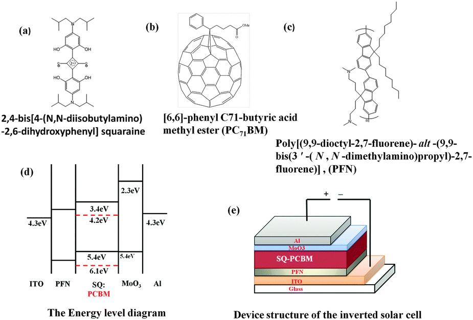 | ||
| Fig. 1 Molecular structure of (a) squaraine, (b) PC71BM, (c) PFN. Schematic of (d) the energy level diagram (e) the device structure of the inverted solar cell. | ||
Experimental section
Materials and methods
All the chemicals and the substrates used for the fabrication were commercially purchased. The devices were fabricated on cleaned indium tin oxide (ITO) coated glass plates (10 Ω cm−2, Delta Technologies Inc, USA). Poly [(9,9-bis(3′-(N,N-dimethylamino)propyl)-2,7-fluorene)-alt-2,7-(9,9-dioctylfluorene)] (PFN, Purity >99%, 1 Materials Canada) was used to modify the work function of ITO to be used as a cathode in the inverted structure. Active layers were made using different blend ratios of 2,4 bis[4-(N,N-diisobutylamino)-2,6-dihydroxyphenyl] squaraine (SQ, Purity >99%, Sigma Aldrich) and [6,6]-phenyl C71 butyric acid methyl-ester (PC71BM, Purity >99%, American Dye Sources, Canada) in ortho-dichlorobenzene (ODCB, Sigma Aldrich, HPLC grade). Thermally evaporated molybdenum trioxide (MoO3, Purity >99%, Sigma Aldrich) was used as a hole transporting, electron blocking interfacial layer. Aluminum was used as a back contact, which was purchased from Sigma Aldrich.Device fabrication and characterization
Devices were fabricated on an ITO coated glass substrate. ITO coated glass plates were cleaned with soap solution and ultrasonicated using deionized water, acetone and isopropyl alcohol for 30 minutes. Cleaned substrates were kept in a vacuum oven overnight for drying. Before spin coating the layers, ITO samples were exposed to UV ozone for about 30 minutes. On top of ITO substrates, PFN was spin coated, which was dissolved in methanol and mixed with acetic acid with a concentration of 0.2 mg ml−1 and then was spin coated at an rpm of 2000 to obtain a thin film of ∼5 nm and is used as an electron transporting, hole blocking layer. Active layers were made using different blend ratios of SQ:PCBM keeping a constant solution concentration (42 mg ml−1) to obtain a uniform thickness of active layers over different devices. The active layer solution was then spin coated (1500 rpm) over the thin PFN layer to form a layer of thickness 100 nm. The thin layer of (7 nm) MoO3 evaporated at a pressure of ∼10−6 torr was used as a hole transporting, electron blocking interfacial layer. Aluminum (Al) of thickness ∼100 nm was thermally evaporated at a base pressure of 10−6 torr and was used as the top electrode. A device structure of ITO/PFN/SQ:PC71BM/MoO3/Al was used for the solar cell studies. The thickness of spin cast films was measured using a Dektak stylus profilometer and that of thermally evaporated materials using an inficon thickness monitor. The active area of the device was 9 mm2. The devices were unencapsulated and all the measurements were performed under ambient conditions using samples mounted on a temperature controlled chuck. The sample temperature was maintained at 25 °C and was monitored using a thermocouple.
The current–voltage characteristics of the devices were performed using a Keithley 6430 source meter in the dark and under the illumination of a 1000 W m−2 AM1.5G spectrum using an Oriel 3A solar simulator tested with a NREL calibrated silicon solar cell. The external quantum efficiency (EQE) measurements were carried out by a lock-in technique using a 250 W xenon lamp coupled with a Newport monochromator and chopped at 40 Hz using a light chopper blade as a light source. A lock-in amplifier (SRS 830, Stanford Research Systems Inc USA) was used to measure currents and a NIST calibrated silicon photodiode was used to find the power spectral response of the incident light. The measurements were performed using shadow masks to avoid edge effects and an appropriate mismatch factor was taken to square off the spectral mismatch for calculating the PCE and EQE.19,20 The intensity dependent measurements were performed using an AM1.5G, 1 Sun light source, in combination with neutral density filters of different optical densities.
Results and discussion
Different SQ:PC71BM ratios were tested to obtain the best performance by considering high absorption coefficient, a broad spectral window extending up to λ ∼ 800 nm and a low exciton diffusion length <6 nm of SQ and a large diffusion length and a poor absorption coefficient of PC71BM.
The best results were obtained for an active layer of ∼100 nm thickness made from 1:6 blend ratios by weight of SQ:PC71BM with an external quantum efficiency (EQE), varying from 45% to 65% in the spectral window extending to λ ∼ 800 nm and a power conversion efficiency (PCE) of 2.45%. We fabricated more than 20 devices in each ratio and more than 50 best performing devices with a SQ:PC71BM blend ratio of 1:6 by weight. The performance of organic photovoltaic cells depends on many parameters such as efficient light absorption, exciton creation, exciton dissociation, free carrier transport, and charge transfer to the electrodes. In order to understand the above-mentioned factors, various electrical and optical measurements were carried out.
The UV VIS absorption spectra of SQ:PC71BM for different blend ratios are shown in Fig. 2a. It is to be noted that we have measured the absorption spectra of thin films of the same thickness (100 nm) as we used in our devices for different blend ratio. The absorption strength of SQ at λ ∼ 683 nm steadily increases as the SQ:PC71BM blend ratio is varied from 1:0.5 to 1:6. This is in spite of the fact that the weight content of SQ in the 1:6 blend ratio is much lower than that in the blend ratio of 1:0.5. This may be due to the well-known fact that SQ dimers or aggregates show lower absorption coefficients compared to monomers.21,22 Or in other words, in a SQ:PC71BM blend ratio of 1:6, SQ is well dispersed in the PC71BM matrix with monomer like features and in other blends it is in dimeric or in aggregate form. A comparison of the UV VIS absorbance of pristine SQ thin films of 100 nm thickness with that of SQ:PCBM blends (1:0.5 blend ratio) is given in Fig. S1 (ESI†). This result clearly shows the aggregation of SQ with a broadened absorption spectrum and the reduced absorbance of SQ only in thin films as compared to SQ:PCBM blends.
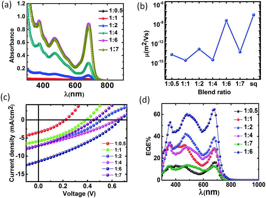 | ||
| Fig. 2 (a) UV-Vis absorption of different ratios of SQ:PC71BM blend (b) hole mobility of squaraine in a pristine film and in a blend with PC71BM in different ratios (c) current density vs. voltage (J–V) characteristics of the SQ:PC71BM devices for different blend ratios, (d) EQE of SQ:PC71BM devices fabricated at different blend ratios. | ||
Along with other parameters, a balanced electron and hole mobility of PC71BM and SQ respectively is necessary to extract free carriers from the BHJ devices. In order to find the best blend ratio for achieving balanced hole and electron transport, SQ:PC71BM blends of different blend ratios were studied. SQ shows a hole mobility of 2.83 × 10⁻⁴ cm2 V−1 s−1 in the pristine form and it further reduces in conjunction with PC71BM. The hole mobility of SQ in the blend film is controlled by the hopping of holes through the SQ domains in the blend.23 Previous reports of zero field mobility of SQ suggest that the performance of the SQ:PC71BM blend was limited by its poor hole mobility through the discontinuous SQ networks compared to the electron mobility through the PC71BM networks.14 We also observe a similar result with the SQ:PC71BM, 1:6 blend ratio, showing a hole mobility nearer to that of pristine SQ compared to other SQ:PC71BM blend ratios. The improved hole mobility of SQ in SQ:PC71BM of blend ratio 1:6 can be attributed to well dispersed SQ in the PC71BM matrix with SQ within the optimized hopping distance.23 This argument is speculated based on the SQ contribution to the UV VIS absorption of different SQ:PC71BM blend ratios and mobility studies. Fig. 2b shows the variation of the hole mobility of SQ in different blend ratios of PC71BM. We find that SQ:PC71BM of the 1:6 blend ratio has a hole mobility much nearer to the electron mobility of PC71BM24,25 and expected to show better OPV performances. The measurement of the hole mobility of SQ is performed by using a hole only device of ITO/PEDOT-PSS/SQ/Au and ITO/PEDOT-PSS/SQ:PC71BM/Au. Mobilities were calculated by fitting the dark IV characteristic with a space charge limited current (SCLC) model. eqn (1) (Fig. S2, ESI†).
 | (1) |
Devices with different SQ:PC71BM blend ratios by weight were fabricated and tested for their photovoltaic properties. The dark I–V and rectification ratio is shown in Fig. S3 and Table S1 (ESI†) respectively. The I–V characteristics of the inverted BHJs for different ratios of SQ:PC71BM in the presence of light are shown in Fig. 2c. The open circuit voltage (VOC), short circuit current density (JSC) and power conversion efficiency (PCE) increase as the SQ:PC71BM ratio varies from 1:0.5 to 1:6 and further it remains constant or deteriorates. The origin of such improvement leading to an increase in VOC, JSC and PCE to 0.68 V, 11.47 mA cm−2, and 2.45%, respectively, for an optimized SQ:PC71BM blend ratio of 1:6 depends on effective transport and transfer of free carriers created upon exciton dissociation in the BHJ OPV.
Photoluminescence (PL) quenching experiments of SQ in the presence of PC71BM show a good quenching of the PL peak of SQ at λ ∼ 688 nm (Fig. 3) even with a small amount of PCBM. The quenching does not vary much with higher PCBM content. This shows an efficient exciton quenching at the SQ:PC71BM interface. EQE of the devices with different blend ratios provide information about the effective extraction of free carriers created by the exciton dissociation at different λ in the spectral window of the SQ:PC71BM blend.
 | ||
| Fig. 3 PL spectra of thin films of pristine SQ, SQ:PCBM blends of blend ratios 1:0.5 and 1:6 excited at 600 nm. | ||
The EQE of the inverted BHJ OPVs with different blend ratios of SQ and PC71BM is shown in Fig. 2d. The EQE shows further contribution from both SQ and PC71BM. By comparing the EQE vs. λ spectra with the absorption spectra (Fig. 2a) of individual SQ and PC71BM, it can be inferred that the photocurrent in the λ range of 300 nm to 600 nm is mostly due to PC71BM with peaks at λ = 360 nm, λ = 484 nm and the photocurrent up to λ ∼ 800 nm is mostly due to SQ with a peak at λ ∼ 680 nm. The EQE of the device increases steadily as the SQ:PC71BM blend ratio is varied from 1:0.5 to 1:6, and for the higher PCBM weight ratio it reduces. The optimized performance of the SQ:PC71BM blend ratio of 1:6 can be due to balanced electron and hole transport. Deviation from this blend ratio results in a poor charge extraction and reduced EQE. This is inferred from the following observations. [(a) If the exciton dissociation was the dominant EQE mechanism, the EQE at λ ∼ 680 nm should be increased or remain the same as the absorption of SQ increases in the blend as the SQ:PC71BM blend ratio is increased from 1:0.5 to 1:7. But here we observe a decrease in EQE at λ ∼ 680 nm as the SQ:PC71BM blend ratio is increased from 1:6 to 1:7. This can be attributed to an imbalanced mobility of electrons and holes in the blend as the hole mobility of SQ is reduced significantly as the SQ:PC71BM blend ratio is varied from 1:6 to 1:7 (which is measured using a SCLC method as shown in Fig. 2b), (b) EQE spectra show peaks at λ ∼ 360 nm, λ ∼ 490 nm and λ ∼ 680 nm similar to the absorption peaks of the blend. Most of the light is absorbed near the PFN/blend interface in the wavelength range of 300 nm < λ < 400 nm and at the MoO3/blend interface in the wavelength range of 600 nm < λ < 800 nm. We expect a bigger ratio of EQE at λ ∼ 360 nm with respect to λ ∼ 680 nm, similar to the absorption profile. But, here we observe a reduced ratio. This can be due to the recombination of holes created at the PFN/Blend interface before reaching the MoO3/blend interface due to mobility mismatch between holes and electrons in the blend. In the case of EQE at λ ∼ 680 nm and λ ∼ 490 nm, holes are created much near the MoO3/blend interface and can be easily extracted to MoO3, without much recombination. On the other hand, the electrons created at the MoO3/blend interface do not face much recombination as they can be easily transported through the PC71BM to PFN/blend. This explains (1) the <1 ratio of EQE at λ ∼ 360 nm with respect to that at λ ∼ 680 nm compared to its >1 ratio of absorption at the respective wavelengths, (2) comparable EQE and absorption ratios for λ ∼ 490 nm with respect to λ ∼ 680 nm.] Our results are in agreement with previous reports where it is mentioned that the EQE mostly depends on the balanced electron and hole mobility in the blend rather than the exciton dissociation.14 For the highest efficiency device (1:6) the average efficiency is about 55% through the UV-Vis and NIR region. The peak efficiency was 65% at λ ∼ 680 nm. The JSC calculated for the highest efficiency device from the EQE spectra by multiplying the EQE spectrum by the standard AM1.5G and integrating it over the wavelength region was in good agreement with the JSC from current voltage (I–V) experiments in the presence of AM 1.5G light of intensity 1 Sun. The calculated JSC was 11.67 mA cm−2, whereas the experimentally (I–V) obtained value for the respective devices was 11.47 mA cm−2.
The VOC of devices with different ratios of SQ:PC71BM is given in Table 1. The VOC increases with increasing PC71BM and an optimum VOC of 0.68 V is observed for devices with the SQ:PC71BM blend ratio of 1:6. Further increase in the PC71BM content decreases the VOC. The extraction of free carriers from the devices increases as the SQ:PC71BM blend ratio is increased from 1:0.5 to 1:6. This can be attributed to reduced recombination due to mismatch between the hole and electron mobility as observed in the mobility measurements of SQ:PC71BM of different blend ratios. Hence the improvement in VOC can be a result of limited recombination in the BHJ OPV and a maximum value of 0.68 V is observed for optimized SQ:PC71BM devices of blend ratio 1:6. Further increase in the PC71BM content modifies the mobility match between the holes and the electrons and results in a recombination limited extraction and reduced VOC. The devices also show a similar trend for JSC with an optimized performance of 11.47 mA cm−2 for SQ:PC71BM devices with a blend ratio of 1:6.
:PC71BM inverted solar cells under 1 Sun illumination
| SQ:PC71BM ratio |
V OC (V) | J SC (mA cm−2) | FF (%) | PCE (%) |
|---|---|---|---|---|
| 1:0.5 |
0.23 | 0.34 | 28.69 | 0.25 |
| 1:1 |
0.38 | 5.86 | 32.12 | 0.78 |
| 1:2 |
0.53 | 7.11 | 28.47 | 1.18 |
| 1:4 |
0.65 | 7.10 | 26.54 | 1.36 |
| 1:6 |
0.68 | 11.47 | 31.62 | 2.45 |
| 1:7 |
0.53 | 7.43 | 28.13 | 0.99 |
Here, in the best performing device, the photocurrent Iph shows KIα dependence on incident light intensity I (where α is the exponential factor and K is a proportionality constant), with α value ∼1 (Fig. 4a). This shows the properties of monomolecular or a geminate recombination mechanism.27,28 in the SQ:PC71BM devices. As the intensity increases VOC increases and saturates for higher intensities (Fig. 4b). The general expression for VOC29 is given in eqn (2).
 | (2) |
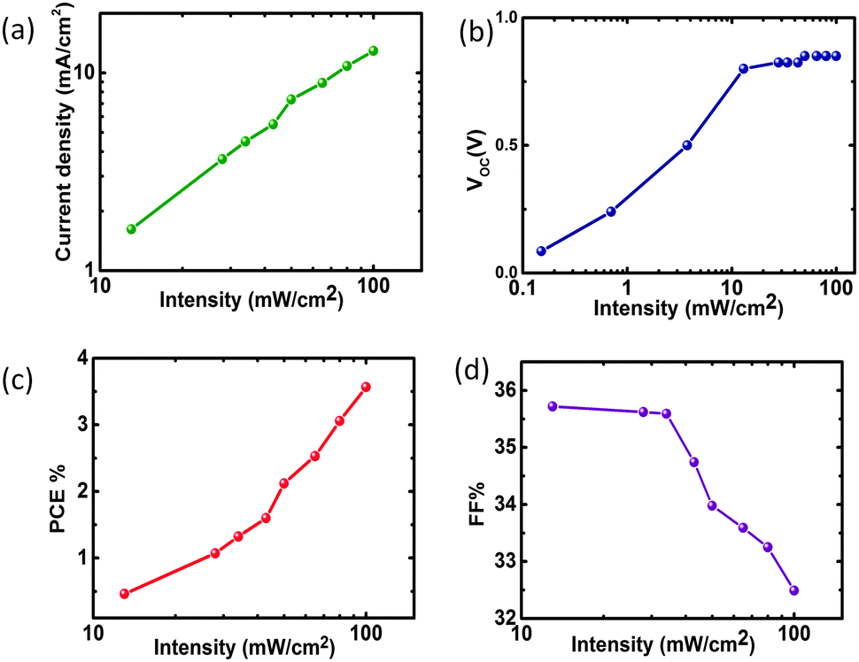 | ||
| Fig. 4 Dependence of (a) JSC (b) VOC (c) PCE% and (d) FF% on illumination intensity of inverted SQ:PC71BM photovoltaic cells blended at 1:6 ratios. | ||
The first term is the effective band gap, ΔEDA, the second term represents disorder induced VOC loss, and the third term represents carrier recombination induced VOC loss. At low intensities n and p vary linearly with intensity and as a result VOC varies logarithmically with intensity. At higher intensity the shunt resistance (Rsh) of the device is reduced30 and hence the term V/Rsh in the practical diode equation for solar cells cannot be neglected (as shown in eqn (3)), where T is the temperature, kB is the Boltzmann constant, m is the diode ideality factor, J0 is the reverse saturation current density, Jph is the photocurrent, V is the output voltage, and Rs is series resistance
 | (3) |
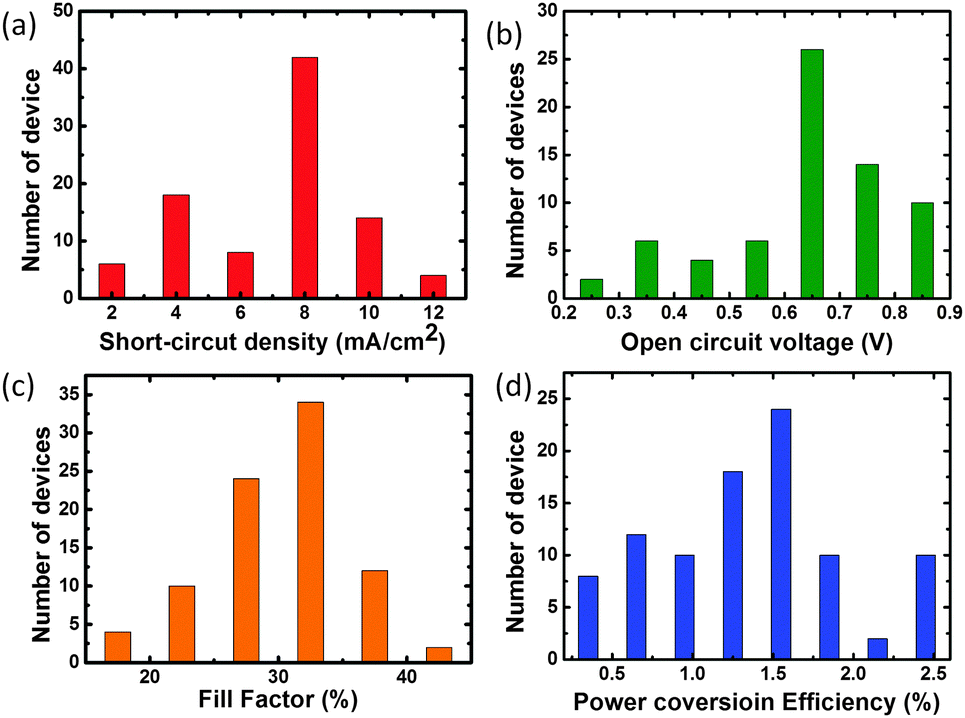 | ||
| Fig. 5 Histogram of the photovoltaic performance parameters such as (a) JSC, (b) VOC, (c) FF% and (d) PCE% of the SQ:PC71BM (1:6) inverted solar cell. | ||
The optimized inverted BHJ OPV shows an enhanced power conversion efficiency of 4.12% upon exposure of the device to AM1.5G light of intensity 1 Sun for 10 minutes, prior to I–V measurements. The PCE vs. exposure time for the device with the blend ratio of 1:6 is shown in Fig. 6a. As the illumination time varies from one to ten minutes, PCE increases from 2.45% to 4.12% and further exposure results in a saturation of PCE at 4%. Devices with other blend ratios exhibit similar behaviour. The EQE spectrum of the device before and after illumination shows an increase in EQE over the entire wavelength region without any distortion in the spectral shape (Fig. 6b). This increase in PCE and EQE upon exposure of light before the measurement can be explained by the enhanced charge carrier transport through the bulk and transfer to the electrode. The reason for the enhanced performance of the device on continuous exposure of light arises from the ITO/PFN interface. The devices were fabricated under ambient conditions; the adsorbed oxygen on the ITO caused the formation of the mid gap charge transfer states in the PFN layer near to the ITO/PFN interface.31 These states increase the work function of ITO by reducing the electric dipole moment within the PFN layer. Upon continuous light exposure, the photon excited electrons fill the mid trap states and restore the reduced dipole moment of PFN. This helps to reduce the work function of ITO as well as the charge extraction barrier, hence showing a better performance. This can be attributed to reduced recombination and enhanced free carrier transport as an improved VOC and JSC was observed while performing I–V measurements after light exposure of the devices. Fig. 7 gives the variation observed in the solar cell parameters with time.
 | ||
| Fig. 6 (a) Illuminated AM1.5G, 1 Sun light exposure time effect on power conversion efficiency of SQ:PC71BM photovoltaic device blended at a 1:6 ratio and the stability of the cell tested on different days. (b) EQE of the SQ:PC71BM (1:6) device before and after continuous illumination of the device under 1 Sun illumination. | ||
 | ||
| Fig. 7 Variation of solar cell parameters (a) JSC, (b) VOC, (c) FF%, (d) PCE% with time. | ||
Further work is in progress to understand the origin of such an enhancement. Prolonged measurements of PCE at certain intervals of time after illumination show a small decrease in the PCE value. The stability of the devices in air was tested for a period of 1 month. The devices were unencapsulated and characterized under ambient conditions. The devices showed good stability under these conditions, with a decrease in efficiency to 2%.
Conclusions
In conclusion, solution processed inverted SQ:PC71BM devices were fabricated and the ratio was optimized as 1:6 with a power conversion efficiency of 2.45%. The devices also showed an enhanced PCE value of 4.12% upon continuous illumination using an AM1.5G light source. The device performance parameters such as VOC, JSC, and EQE were studied in detail and correlated with the spectroscopy studies of SQ in the presence of PC71BM. The device showed spectral response with an EQE varying from 45% to 65% over a broad solar spectral window extending to the NIR region. Intensity dependent measurements of devices showed monomolecular recombination as one of the limiting factors of the performance of the device. The air processed device showed reasonable stability for a period of one month.
Acknowledgements
We acknowledge funding from the Department of Science and Technology (DST/TM/SERI/2k11/73(G)), the Solar Energy Research Initiative project, and the Ministry of Human Resource Development both under Govt. of India.Notes and references
- A. Treibs and K. Jacob, Angew. Chem., Int. Ed., 1965, 4, 694 CrossRef.
- A. Ajayaghosh, Acc. Chem. Res., 2005, 38, 449 CrossRef CAS PubMed.
- A. C. Tam, Appl. Phys. Lett., 1980, 37, 78 CrossRef.
- C. W. Dirk, W. C. Herndon, F. Cervantes-Lee, H. Selnau, S. Martinez, P. Kalamegham, A. Tan, G. Campos and M. Velez, J. Am. Chem. Soc., 1995, 117, 2214 CrossRef CAS.
- G. J. Ashwell, G. Jefferies, D. G. Hamilton, D. E. Lynch, M. P. S. Roberts, G. S. Bahra and C. R. Brown, Nature, 1995, 375–385 Search PubMed.
- V. Y. Merritt and H. J. Hovel, Appl. Phys. Lett., 1976, 29, 414 CrossRef CAS.
- D. L. Morel, A. K. Ghosh, T. Feng, E. L. Stogryn, P. E. Purwin, R. F. Shaw and C. Fishman, Appl. Phys. Lett., 1978, 32, 495 CrossRef CAS.
- B. Walker, C. Kim and T.-Q. Nguyen, Chem. Mater., 2010, 23, 470 CrossRef.
- J. Roncali, Acc. Chem. Res., 2009, 42, 1719 CrossRef CAS PubMed.
- S. Sreejith, P. Carol, P. Chithra and A. Ajayaghosh, J. Mater. Chem., 2008, 18, 264 RSC.
- G. Chen, D. Yokoyama, H. Sasabe, Z. Hong, Y. Yang and J. Kido, Appl. Phys. Lett., 2012, 101, 083904 CrossRef.
- S. Wang, E. I. Mayo, M. D. Perez, L. Griffe, G. Wei, P. I. Djurovich, S. R. Forrest and M. E. Thompson, Appl. Phys. Lett., 2009, 94, 233304 CrossRef.
- G. Chen, H. Sasabe, Z. Wang, X.-F. Wang, Z. Hong, Y. Yang and J. Kido, Adv. Mater., 2012, 24, 2768 CrossRef CAS PubMed.
- G. Wei, S. Wang, K. Renshaw, M. E. Thompson and S. R. Forrest, ACS Nano, 2010, 4, 1927 CrossRef CAS PubMed.
- G. Wei, S. Wang, K. Sun, M. E. Thompson and S. R. Forrest, Adv. Energy Mater., 2011, 1, 184 CrossRef CAS.
- D. Bagnis, L. Beverina, H. Huang, F. Silvestri, Y. Yao, H. Yan, G. A. Pagani, T. J. Marks and A. Facchetti, J. Am. Chem. Soc., 2010, 132, 4074 CrossRef CAS PubMed.
- Z. He, C. Zhong, S. Su, M. Xu, H. Wu and Y. Cao, Nat. Photonics, 2012, 6, 591 Search PubMed.
- R. Xia, D.-S. Leem, T. Kirchartz, S. Spencer, C. Murphy, Z. He, H. Wu, S. Su, Y. Cao, J. S. Kim, J. C. de Mello, D. D. C. Bradley and J. Nelson, Adv. Energy Mater., 2013, 3, 718 CrossRef CAS.
- H. J. Snaith, Nat. Photonics, 2012, 6, 337 CrossRef CAS.
- E. Zimmermann, P. Ehrenreich, T. Pfadler, J. A. Dorman, J. Weickert and L. Schmidt-Mende, Nat. Photonics, 2014, 8, 669 CrossRef CAS.
- N. J. Turro, Modern Molecular Photochemistry, 1991 Search PubMed.
- N. S. S. Kumar, S. Varghese, C. H. Suresh, N. P. Rath and S. Das, J. Phys. Chem. C, 2009, 113, 11927 CAS.
- A. H. Abou El Ela and H. H. Afifi, Phys. Chem. Solids, 1979, 40, 257 CrossRef.
- B. Ebenhoch, S. A. J. Thomson, K. Genevicius, G. Juška and I. D. W. Samuel, Org. Electron., 2015, 22, 62 CrossRef CAS.
- P. Cheng, Y. Li and X. Zhan, Energy Environ. Sci., 2014, 7, 2005 CAS.
- P. W. M. Blom, M. J. M. de Jong and J. J. M. Vleggaar, Appl. Phys. Lett., 1996, 68, 3308 CrossRef CAS.
- P. Schilinsky, C. Waldauf and C. J. Brabec, Appl. Phys. Lett., 2002, 81, 3885 CrossRef CAS.
- V. D. Mihailetchi, J. Wildeman and P. W. M. Blom, Phys. Rev. Lett., 2005, 94, 126602 CrossRef CAS PubMed.
- J. C. Blakesley and D. Neher, Phys. Rev. B: Condens. Matter Mater. Phys., 2011, 84, 075210 CrossRef.
- B. P. Rand, D. P. Burk and S. R. Forrest, Phys. Rev. B: Condens. Matter Mater. Phys., 2007, 75, 115327 CrossRef.
- C.-Y. Nam, J. Phys. Chem. C, 2014, 118, 27219 CAS.
Footnote |
| † Electronic supplementary information (ESI) available: Comparison of UV-VIS absorbance data of pristine SQ and SQ:PCBM blends of the same thickness, SCLC fitting of dark IV characteristics of hole only devices, Dark I–V characteristics of devices and the rectification ratio of the devices. See DOI: 10.1039/c5cp05080d |
| This journal is © the Owner Societies 2016 |