 Open Access Article
Creative Commons Attribution 3.0 Unported Licence
Increased carrier mobility in end-functionalized oligosilanes†
S.
Surampudi
a,
M.-L.
Yeh
ab,
M. A.
Siegler
a,
J. F. Martinez
Hardigree
b,
T. A.
Kasl
a,
H. E.
Katz
ab and
R. S.
Klausen
*a
aDepartment of Chemistry, Johns Hopkins University, 3400 N. Charles St, Baltimore, MD 21218, USA. E-mail: klausen@jhu.edu
bDepartment of Materials Science and Engineering, Johns Hopkins University, 3400 N. Charles St, Baltimore, MD 21218, USA
First published on 5th January 2015
Abstract
We show that a class of oligosilane–arene σ, π-hybrid materials exhibits distinct and enhanced solid-state electronic properties relative to its parent components. In the single crystal structure, the σ-conjugation axis of one molecule points towards the π-face of a neighboring molecule due to an unusual gauche conformation. This organization is hypothesized to be beneficial for charge transport. We show that solution-deposited crystalline films of the hybrid materials show up to a 100-fold increase in space-charge limited current (SCLC) mobility relative to literature reports of photoinduced hole transport in oligosilane films. The discovery that σ, π-hybrids are more than the sum of their parts offers a design opportunity for new materials.
Introduction
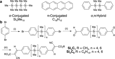
The ordering of individual molecules in a solid is as important for efficient charge transport as the electronic properties of the molecule itself. This manuscript describes a new, close-packed molecular crystal form exhibited by oligosilanes terminated with cyanovinyl groups. We report record-setting oligosilane charge carrier mobilities in their crystalline thin films.Crystalline silicon is the preeminent semiconductor. While molecular variants of other extended materials are well developed for electronic applications (for example, the pentacene1–3 core is a substructure of the graphitic carbon lattice), oligosilanes are not broadly studied as small molecule semiconductors. Nonetheless, oligosilanes have attractive properties that merit consideration. Permethylsilanes (SinMe2n+2, Fig. 1)4 are the simplest organosilanes and are bench-stable, processable in organic solvents and absorb light strongly in the ultraviolet region due to delocalized σ molecular orbitals.5,6 Molecular silanes retain the practical attractions of silicon itself, like earth abundance and low toxicity. Lastly, the potential for structural variation is enormous. As part of a program dedicated to identifying the structural requirements for facile charge transport in silanes, here we focus on the integration of molecular silicon with functionalized π-conjugated organic groups.
Results and discussion
Design and synthesis
Tetra- and hexasilanes were selected for initial study on the basis of structure–property relationships identified in photoinduced hole transport studies of oligosilanes7 and polysilanes8 (μ = 10−4 to 10−3 cm2 V−1 s−1). Okumoto et al. in a time-of-flight study of polycrystalline SinMe2n+2 (n = 8–12) films showed that mobility is lower in odd-numbered than even-numbered silane films and that mobility increases with oligosilane length (Si8Me18, μ ≅ 7.5 × 10⁻⁴ cm2 V−1 s−1).7 Kepler et al. observed similar magnitude hole mobilities in poly(SiMePh) and poly(Si(n-Pr)2) films (μ = 10−4 cm2 V−1 s−1), but poly(SiMePh) devices were more photostable.8To further elucidate substituent effects, we installed terminal functionalized arenes, which also increase crystallinity. We particularly focused on cyanovinyl groups, an archetypal electron acceptor moiety.9,10 Thienyloligosilanes and polymers have previously been described.11,12 α,ω-Dichlorooligosilanes of defined length were synthesized and then arylated with 4-bromophenyllithium according to Tamao's literature procedure (Fig. 1b).13,14 Subsequent lithium–halogen exchange, formylation with N,N-dimethylformamide, and Knoevenagel condensation with methyl 2-cyanoacetate yields cyanovinylsilanes Si4C1 and Si6C1. Use of n-hexyl 2-cyanoacetate in the Knoevenagel condensation yields Si4C6 and Si6C6. Gratifyingly, all products are crystalline solids at room temperature. Products are exclusively the (E)-olefin isomer, as determined by 2-D NMR spectroscopy and single crystal X-ray diffraction (XRD).
Unusual gauche-conformation in crystal structure
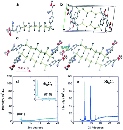
The single crystal XRD structures of Si4C1 and Si6C1 show that one terminal arene is gauche relative to the silane chain (Fig. 2a), a highly unusual conformation. Most acyclic α,ω-arylmethylsilanes in the Cambridge Crystallographic Database adopt a fully extended, all-trans structure and a more limited number have eclipsed conformations.14,15 A complete list of references to relevant crystal structures can be found in the ESI.† A single crystal XRD structure of an acyclic permethylsilane has not been reported, but the powder XRD pattern of a vacuum-deposited Si12Me26 thin film shows a d-spacing (d = 25.9 Å) consistent with all-anti-silanes oriented perpendicular to the substrate.16Two molecules of gauche-Si6C1 pack such that cyanovinylarene groups co-facially localize and the resultant dimer constitutes the unit cell (Fig. 2b). The distance between carbonyl carbons in neighboring dimers along the c direction is short (3.44 Å, Fig. 2c). We prepared solution-deposited crystalline films by drop-casting a 1,2-dichlorobenzene oligosilane solution onto a Si/SiO2 substrate. The XRD pattern of the Si6C1 thin film is consistent with a polycrystalline film in which silanes are oriented both perpendicular and parallel to the substrate. The most intense peak in the Si6C1 powder XRD pattern (Fig. 2d, 2θ = 4.67°, d = 18.9 Å) is consistent with the c-axis of the Si6C1 unit cell (20.4 Å) and is therefore assigned to reflection from the (001) plane. A lower intensity peak (2θ = 7.71°, d = 11.5 Å) is assigned to reflection from the (010) plane (b-axis = 11.8 Å).
While we were unsuccessful in obtaining a single crystal XRD structure of Si6C6 or Si4C6, the thin film XRD patterns are not consistent with a fully extended conformation. The intense reflection at 2θ = 6.47° corresponds to a d-spacing of 13.7 Å, significantly shorter than the predicted fully extended molecular length of >41.0 Å (see ESI† for more details). Peaks in the Si6C6 powder XRD pattern are much more intense than in the Si6C1 film, suggesting that Si6C6 forms the more well-ordered film with larger domains, a hypothesis supported by optical microscopy and atomic force microscopy (vide infra).
Increased charge carrier transport
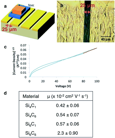
In the Si6C1 structure, the gauche conformation allows for a close-packed structure and the intermolecular spacing in the c-axis direction is short (3.44 Å). Charge transport in the c-axis direction could therefore be particularly efficient as the c-axis is also aligned with the σ-conjugation axis. We fabricated devices to characterize electronic properties (Fig. 3a). Gold electrodes (50 nm) were thermally evaporated onto clean glass slides with a 25 μm tungsten wire shadow mask. The wires were removed and a rectangular pattern (1 × 2.5 mm) defined on the electrodes with Novec™ 1700 Electronic Grade Coating. A 1,2-dichlorobenzene solution of oligosilane was drop-cast onto the Novec™ pattern, then sequentially dried in ambient conditions and in a vacuum oven. A transparent, crystalline film covers the 25 μm channel (Fig. 3b). Current–voltage characteristics were measured and the charge carrier mobility extracted from the space-charge limited current (SCLC) regime of the J1/2–V plot using the Mott–Gurney law (Fig. 3c and ESI†).17 We observe, as did Okumuto et al.,7 that the mobility increases with silane length.More unusually, we observe an increase in mobility with increasing the length of the ester alkyl chain (Si6C1 < Si6C6 and Si4C1 < Si4C6, Fig. 3d). This is in distinct contrast to Okumoto's study showing a decrease in mobility in anti-silane films with longer alkyl groups due to increased interlayer distances.18 That we observe the opposite trend is supportive of the hypothesized beneficial effect of the gauche-conformation.
In solution, Si6C1 and Si6C6 have identical optical and electronic properties. The dependence of device mobility on alkyl chain length is therefore attributed to the increased crystallinity of the thin film as detected by XRD analysis (Fig. 2d and e).
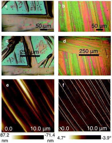
Optical and atomic force microscopy images confirm the superior film structure. The drop cast Si6C1 film contains both relatively large (100–150 μm wide) needles and precipitated islands (Fig. 4a and c). In contrast, the optical microscope image of the Si6C6 thin film shows a highly oriented smooth and continuous polycrystalline film (Fig. 4b and d). The Si6C6 thin film was further characterized by atomic force microscopy (AFM) (Fig. 4e and f). Both the AFM height and phase images show oriented, smooth regions and are consistent with a lamellar sheet morphology. Additional images are available in the ESI.†
The combination of silane length and desirable film morphology makes the Si6C6 SCLC mobility (μ = 0.023 cm2 V−1 s−1) the highest mobility measured in this system or in any molecular silane. High carrier mobility is also observed in preliminary thin film transistor studies. Three devices with a Si6C6 active layer and width-to-length ratios between 10 and 20 showed transistor-like output curves, from which mobilities between 0.01 and 0.06 cm2 V−1 s−1 were calculated, consistent with the SCLC values (see ESI†).
The carrier mobilities in this study are 1–2 orders of magnitude greater than previous reports, an especially notable result given that our oligosilanes (n = 4–6) are shorter than those previously characterized (n ≥ 8) and mobility increases with silane length. The observed carrier mobilities likely represent the lower limit of the carrier mobility because of the polycrystalline nature of the thin films investigated and the hypothesized anisotropy in charge transport.
Alkyl-linked cyanovinylarenes are less effective charge transport materials
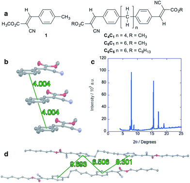
Alkane control molecules (Fig. 5a) strongly point to an essential structural and electronic role for the silane moieties in the hybrid materials. We find that the parent arene 1 adopts a slip-stacked structure in which centroids are separated by 4.00 Å (Fig. 5b), a very different packing structure from gauche-silanes. XRD analysis of a solution-deposited thin film of 1 shows high intensity, narrow peaks consistent with a polycrystalline structure (Fig. 5c). However, electronic characterization of devices fabricated in the same manner as the cyanovinylsilanes did not show a SCLC region and charge carrier mobility could not be determined (see the ESI† for more details). C6C6 (Fig. 5a), an analog of Si6C6, was synthesized and characterized as well. Widely displaced and separated aryl rings are observed in the C6C6 crystal structure (Fig. 5d). Current–voltage characterization does not show a SCLC region in devices prepared from C4C1, C6C1, nor C6C6.†Density functional theory calculations
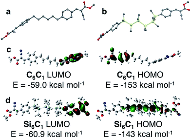
The structural role of the silane was further investigated by quantum chemical calculations (B3LYP/6-31G) of C6C1 and Si6C1. The optimized gas phase structure of an isolated C6C1 molecule is different from its crystal structure conformation (Fig. 6a). In the gas phase, linker chains adopt an all-anti conformation. The terminal arenes are in line with the linker axis, but the arene planes are perpendicular. Clearly, the kink in the alkane linker observed in the C6C6 crystal structure is supported by intermolecular interactions. Intermolecular CH–π interactions involving the alkane linker are found in the C6C6 crystal structure and are illustrated in Fig. S3 (see the ESI† for more details).Quantum chemical calculations of Si6C1 are computationally intensive because of the six heavy elements and the additional degrees of freedom introduced by the silane methyl substituents. The calculations have difficulty converging on a single optimized geometry. One low energy conformation (Fig. 6b) has a gauche conformation within the silane chain itself (ω = 57.7°), a conformation different from both the Si6C1 crystal structure and the all-anti C6C1 optimized geometry. Other low energy conformations of Si6C1 have an all-anti relationship. We interpret the computational data to mean that rotation about the Si–Si bond in the gas phase is facile. We suggest that in the bulk material, the flexible oligosilane chain can easily adjust to accommodate stabilizing interactions with neighbouring functional groups, which drive the preference for the gauche-cyanovinylsilane conformation in the crystal structure. Fig. S4† highlights some of the intermolecular short contacts between Si6C1 molecules in the unit cell.
Our results are consistent with the body of theoretical studies on oligosilane structure that show a flat conformational profile.4,19,20 Studies by West and others report that both gauche and anti conformations are energy minima and differ by <1 kcal mol−1. The calculated barrier to rotation is small (∼1 kcal mol−1).19
Because of the well-known dependence of oligosilane electronic structure on conformation,21,22 it is difficult to compute a reliable Si6C1 electronic structure for comparison with C6C1 in view of the similar energies of multiple Si6C1 conformations. Nevertheless, we present one possible pairwise comparison here. In C6C1, the HOMO and LUMO are localized on opposite arenes and no orbital density is found on the alkane chain (Fig. 6c). In gauche-Si6C1, we find that the LUMO is also localized on one arene, while the HOMO is delocalized across the hexasilane (Fig. 6d). The alternating nodal pattern reproduces the electronic structure of simple permethyl and perhydrohexasilanes.4,23
The difference in the Si6C1 and C6C1 HOMO energies supports an electronic role for silicon. This is also strongly suggested by a visual comparison of the alkyl and silyl materials: the silanes are bright yellow in color, while the alkyl materials are white. A donor–acceptor interaction between the silane and the cyanovinyl group is consistent with intermolecular charge transfer from cyclosilanes to tetracyanoethylene identified by EPR studies.24,25 Intramolecular charge transfer studies have focused on the use of silanes as the bridge in donor-bridge–acceptor systems26 and nonlinear optical effects in these systems have been characterized.27
Conclusions
We report here that the combination of σ- and π-conjugated units is greater than the sum of its parts. We observe electronic and structural properties in hybrid materials that cannot be achieved by either unit alone. This observation is expected to be of general interest to the electronic materials community. Our results indicate that further structural optimization of molecular silicon and hybrid materials could yield even greater advances in electronic properties.Acknowledgements
S. S., M.-L. Y., T. A. K., and R. S. K. thank Johns Hopkins University for start-up funds. H. E. K. was supported by the National Science Foundation Division of Materials Research (DMR) (Grant 1005398). We thank the National Science Foundation Division of Materials Research (DMR), MRSEC program, grant number 1121288 for the AFM study. We thank Dr Michael L. Steigerwald for helpful discussions. We thank Jiawang Zhou and Justin DeFrancisco of Johns Hopkins University for assistance with DFT calculations.Notes and references
- O. D. Jurchescu, M. Popinciuc, B. J. van Wees and T. T. M. Palstra, Adv. Mater., 2007, 19, 688 CrossRef CAS.
- S. K. Park, T. N. Jackson, J. E. Anthony and D. A. Mourey, Appl. Phys. Lett., 2007, 91, 063514 CrossRef PubMed.
- C. S. Kim, S. Lee, E. D. Gomez, J. E. Anthony and Y.-L. Loo, Appl. Phys. Lett., 2008, 93, 103302 CrossRef PubMed.
- R. D. Miller and J. Michl, Chem. Rev., 1989, 89, 1359 CrossRef CAS.
- H. Tsuji, J. Michl and K. Tamao, J. Organomet. Chem., 2003, 685, 9 CrossRef CAS.
- A. Bande and J. Michl, Chem.– Eur. J., 2009, 15, 8504 CrossRef CAS PubMed.
- H. Okumoto, T. Yatanabe, A. Richter, J. Peng, M. Shimomura, A. Kaito and N. Minami, Adv. Mater., 2003, 15, 716 CrossRef CAS.
- R. G. Kepler, J. M. Zeigler, L. A. Harrah and S. R. Kurtz, Phys. Rev. B: Condens. Matter Mater. Phys., 1987, 35, 2818 CrossRef CAS.
- H. E. Katz and M. L. Schilling, J. Org. Chem., 1991, 56, 5318 CrossRef CAS.
- H. E. Katz, M. L. Schilling, W. R. Holland, T. Fang, H. M. Gordon and L. A. King, Macromolecules, 1991, 24, 1201 CrossRef CAS.
- J. Ohshita, Y. Izumi, D.-H. Kim, A. Kunai, T. Kosuge, Y. Kunugi, A. Naka and M. Ishikawa, Organometallics, 2007, 26, 6150 CrossRef CAS.
- J. Ohshita, Y. Hatanaka, S. Matsui, T. Mizumo, Y. Kunugi, Y. Honsho, A. Saeki, S. Seki, J. Tibbelin, H. Ottosson and T. Takeuchi, Dalton Trans., 2010, 39, 9314 RSC.
- M. Sasaki, Y. Shibano, H. Tsuji, Y. Araki, K. Tamao and O. Ito, J. Phys. Chem. A, 2007, 111, 2973 CrossRef CAS PubMed.
- R. S. Klausen, J. R. Widawsky, M. L. Steigerwald, L. Venkataraman and C. Nuckolls, J. Am. Chem. Soc., 2012, 134, 4541 CrossRef CAS PubMed.
- T. Sanji, A. Yoshiwara, T. Kibe and H. Sakurai, Silicon Chem., 2003, 2, 151 CrossRef CAS.
- T. Yatanabe, A. Kaito and Y. Tanabe, Chem. Lett., 1997, 799 CrossRef.
- N. F. Mott and R. F. Gurney, Electronic Processes in Ionic Crystals, Clarendon Press, Oxford, 2nd edn, 1948 Search PubMed.
- H. Okumoto, A. Richter, M. Shimomura, A. Kaito and N. Minami, Synth. Met., 2005, 153, 297 CrossRef CAS PubMed.
- J. W. Mintmire and J. V. Ortiz, Macromolecules, 1988, 21, 1991 CrossRef.
- R. West and J. R. Damewood, Macromolecules, 1985, 18, 159 CrossRef.
- H. Tsuji, J. Michl and K. Tamao, J. Organomet. Chem., 2003, 685, 9 CrossRef CAS.
- A. Bande and J. Michl, Chem.– Eur. J., 2009, 15, 8504 CrossRef CAS PubMed.
- A. Herman, B. Dreczewski and W. Wojnowski, Chem. Phys., 1985, 98, 475 CrossRef CAS.
- V. Traven and R. West, J. Am. Chem. Soc., 1973, 95, 6824 CrossRef CAS.
- H. Sakurai, M. Kira and T. Uchida, J. Am. Chem. Soc., 1973, 95, 6826 CrossRef CAS.
- H. Rautz, H. Stuger, G. Kickelbick and C. Pietzsch, J. Organomet. Chem., 2001, 627, 167 CrossRef CAS.
- G. Mignani, A. Kramer, G. Puccetti, I. Ledoux, G. Soula, J. Zyss and R. Meyrueix, Organometallics, 1990, 9, 2640 CrossRef CAS.
Footnote |
| † Electronic supplementary information (ESI) available: Synthetic procedures, tabulated characterization data, single crystal X-crystallography, differential scanning calorimetry thermograms, optical and force microscopy, optical and electronic characterization and device fabrication procedures. CCDC 1030984–1030987. For ESI and crystallographic data in CIF or other electronic format see DOI: 10.1039/c4sc03274h |
| This journal is © The Royal Society of Chemistry 2015 |

