DOI:
10.1039/C5AN00187K
(Paper)
Analyst, 2015,
140, 3262-3272
Self-calibrating highly sensitive dynamic capacitance sensor: towards rapid sensing and counting of particles in laminar flow systems
Received
28th January 2015
, Accepted 5th March 2015
First published on 5th March 2015
Abstract
In this report we propose a sensor architecture and a corresponding read-out technique on silicon for the detection of dynamic capacitance change. This approach can be applied to rapid particle counting and single particle sensing in a fluidic system. The sensing principle is based on capacitance variation of an interdigitated electrode (IDE) structure embedded in an oscillator circuit. The capacitance scaling of the IDE results in frequency modulation of the oscillator. A demodulator architecture is employed to provide a read-out of the frequency modulation caused by the capacitance change. A self-calibrating technique is employed at the read-out amplifier stage. The capacitance variation of the IDE due to particle flow causing frequency modulation and the corresponding demodulator read-out has been analytically modelled. Experimental verification of the established model and the functionality of the sensor chip were shown using a modulating capacitor independent of fluidic integration. The initial results show that the sensor is capable of detecting frequency changes of the order of 100 parts per million (PPM), which translates to a shift of 1.43 MHz at 14.3 GHz operating frequency. It is also shown that a capacitance change every 3 μs can be accurately detected.
Introduction
The ever increasing demand for an “all-electrical” bio-sensing approach has prompted the exploration of new research avenues for biological purposes and medical diagnostics. Electrical sensing techniques have the potential to circumvent the shortcomings of labelled optical techniques.1–3 Static amperometric sensors,4,5 low-frequency spectroscopy,2,6 high-frequency or microwave sensing techniques7–10 are some of the electrical approaches explored so far. The advantages of an individual approach are application specific. Low-frequency impedance analysis is often used for the detection of intra-cellular properties of cells like membrane capacitance,2 but is often governed by the inclusion of bulky reference electrodes in experimental setups. Thus, the miniaturization of integrated systems with such sensors is a far-fetched dream. Additionally, in order to detect the concentration of particles in a suspension such low-frequency impedance sensing might fail to give realistic results due to several dispersion mechanisms.11 Amperometric sensing schemes based on redox cycling have shown promising results for particle counting and single particle sensing,12 but are also governed by bulky reference electrodes for accurate measurements. Amperometric techniques also rely on an extremely slow fluid flow rate for maximum redox cycling, thus making measurement times impractically long. Microwave or high-frequency techniques applied to the detection of cells or particles in a suspension help to avoid low-frequency dispersion issues and also aid in miniaturization of the integrated system. Bulky test-benches and reference electrodes are not required in high-frequency sensing schemes. However, the output handling of such sensors, which includes a complex scattering matrix for passive microwave structures7 and a high-frequency output for reactance based sensors,8 makes data processing tedious. Integrated solutions on CMOS platforms were explored,13,14 however, with sensing at lower frequencies. Therefore, an integrated compact sensor solution with easy signal processing and handling capability added with high measurement speed is still on the horizon.
In this work, we propose a compact BiCMOS label free capacitive sensor approach, where the sensing principle exploits microwave frequencies and at the same time provides a pseudo DC output. An analytical model is established to depict the operation of the capacitive sensor in conjunction with a flow assisted fluidic system. The functionality of the sensor system is further demonstrated using a modulating capacitor emulating the flow of particles in a fluid system. The proposed approach is suitable for particle counting and single particle sensing applications, as the capacitance modulation due to particle flow in a fluid system is analogous to a modulating capacitor, as used in this work. The sensing principle is based on a capacitive sensor embedded in an oscillator circuit. The operating frequency of the sensor is in the range of 12 GHz to 14.5 GHz, thus exploiting the advantages of a high-frequency sensing approach. The frequency modulation of the oscillator due to the capacitance change is read out using a demodulator circuit. Therefore, the output of the sensor is a pseudo DC (few kHz) signal, making handling of the sensor extremely flexible. All in all, the proposed sensor system adds the advantages of high-frequency detection technique, and miniaturization, while simultaneously keeping the output handling capability simple. Moreover, the topology opens the possibility of integrating functionalities such as in situ signal processing, making these chips even more attractive. The measurement time of the sensor is dependent on the settling time of on-chip circuit blocks and can be reduced to the order of a few microseconds. Therefore, the measurement time can be reduced considerably compared to other aforementioned techniques. The theory has been further extended to address the problem of noise in such integrated microfluidic systems. Noise from the sensor circuit and also from the external biological environment plays a crucial role in such devices. Noise can be eliminated by using a correlation technique using two such demodulator architectures with the same integrated system. The recent integration possibilities of these sensor chips with MEMS-based microfluidic systems adds more relevance to such sensors being used in biosensing.15,16 Therefore, the high-frequency microelectronics-based fluidic sensor circuits with DC output handling can be suggested as a promising tool for the miniaturization of conventional biological cell detection techniques.
System dynamics analysis
In our previous works8,17,18 the capacitance change of a planar interdigitated electrode (IDE) structure based on its dielectric ambient in a static fluid condition was shown. When embedded in an oscillator circuit the capacitance change of the IDE results in a shift of the resonant frequency of the oscillator. In this work, we propose an advanced circuitry and an analytical theory to extend the capacitive sensing technique based on a frequency shift sensor towards a flow assisted fluidic system. The extension to a dynamic approach is brought by the inclusion of demodulator circuitry to detect the frequency modulation that would be caused by the dynamic capacitance shift due to the flow of particles in the fluid system. The sensor is designed to operate in the frequency range of 12 GHz to 14.3 GHz, with the demodulator output in the range of a few kHz.
The system is modelled in two steps: in the first step the dynamic capacitance change of the IDE due to particle flow in an aqueous solution is modelled and simulated. In the subsequent step the demodulator circuitry for the detection of the dynamic particle flow is mathematically modelled and simulated.
Modelling of dynamic capacitance sensor
A long fluid channel aligned on top of the sensor with inlets and outlets considerably far from the sensor was considered for modelling. Such a configuration has been previously fabricated for static detection methods18 and a test structure is shown in Fig. 1. In the long-channel condition, suspended particles in the laminar flow of the aqueous solution are in a steady state when they reach the sensor.19,20
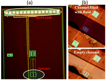 |
| | Fig. 1 Previously fabricated sensor chip with long channel microfluidic system integration. (a) High-frequency sensor chip showing the sensor arrangement. (b) A long channel microfluidic channel is aligned on top of the sensor. The two conditions depict the channel with and without the fluid. | |
The capacitance modulation can be attributed to the inflow and outflow of particles (for e.g. cells in biological suspensions) on top of the sensor as shown in Fig. 2, top. (The section “fabrication of sensor system” gives a detailed overview of the substrate and metals used). The 2D geometry of the IDE sensor structure along with the simulated variation of its capacitance due to a particle flowing over the top of it is shown in Fig. 2, bottom. In our work, the IDE fingers are 5 μm wide, with an equal spacing of 5 μm. A particle of diameter 8 μm (diameter of a standard yeast cell) and permittivity 20 is considered, flowing in an aqueous solution of permittivity 40. Such permittivity values are pragmatic assumptions, as the aqueous solution, which is generally a solution of water, tends to have similar permittivity values at the operating frequency range. As the particle migrates over the top of the sensor, the capacitance reduces as shown in Fig. 2, bottom. This can be attributed to the lower permittivity of the particles compared to the suspending aqueous solution. A steady flow of such particles will, therefore, cause capacitive pulses.
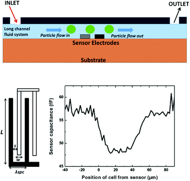 |
| | Fig. 2 (Top) Schematic depiction of particle flow in a long channel fluid system aligned on top of the sensor. (Bottom) Geometry of IDE sensor considered in this work. Simulated variation of sensor capacitance due to the flow of particles. The variation of capacitance is plotted with respect to the position of a particle on top of the sensor. | |
Embedded in the oscillator these capacitive pulses will translate to frequency modulation. The modulation rate is defined by the concentration and velocity of the particles. In the context of sensing, the detection of this frequency modulation will enable particle counting. This dynamic behaviour of the capacitive sensor based on the particle flow can be sensed using an integrated phase-locked loop (PLL) demodulator in conjunction with the sensor embedding oscillator circuit.
In a typical PLL circuit, the output frequency of a voltage-controlled oscillator (VCO) is stabilized by a reference, typically a crystal oscillator.21 In this approach it can be understood that the VCO is replaced by a permittivity controlled oscillator, where the capacitance of the variable capacitor in the oscillator is a function of permittivity instead of voltage. When the resonant frequency of the oscillator is modulated by a moving particle, or by particles of different type, the PLL output frequency is stabilized by a control voltage, which serves as the demodulator output.
Design of the sensor circuit
As mentioned above, a VCO-based reactance sensor, also referred to as a permittivity controlled oscillator, is used for the frequency modulation (FM) sensing together with the demodulator read-out. The sensor capacitor (IDE) is coupled with inductors to constitute a resonator. The oscillation of the resonator is driven by a pair of cross-coupled nMOS transistors as shown in Fig. 3. The resonance frequency of the oscillator is a function of the permittivity of the surroundings of the IDE, which includes the top of the IDE, the oxide in between the fingers and the substrate. The resonance frequency of the oscillator is therefore a function of the permittivity of the IDE's environment. The CMOS cross-coupled oscillator is further embedded in a PLL to demonstrate the proposed technique of frequency modulation–demodulation. The sensor IDE is employed along with three variable capacitors (varactors) in order to modify the oscillation frequency. A large coarse-tuning capacitor Ccoarse is responsible for the compensating Process-Voltage-Temperature (PVT) variations.22 A small fine-tuning capacitor Cfine is used to detect small frequency changes. Moreover, an additional small varactor Cmod is used to emulate the dynamic capacitance change for the initial measurements independent of an integrated microfluidic channel. The buffer stage is used to isolate the oscillator from the subsequent circuit chain following the oscillator.
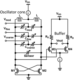 |
| | Fig. 3 Schematic of the sensor circuit. The sensor is embedded in the oscillator circuit. The variable capacitor, Cmod, is used for experiments without fluid integration. | |
Frequency demodulator architecture and analysis
The block diagram of the demodulator architecture used for the read-out of the frequency modulation is shown in Fig. 4. For a detailed understanding of the circuit the readers are referred to research works based on circuit theory and applications.22,23 However, a brief overview of the architecture is given with more emphasis on the modelling and analytical derivation of the differential equations governing the frequency demodulation architecture.
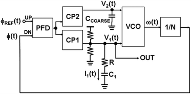 |
| | Fig. 4 Demodulator architecture block diagram. The output of the demodulator is taken from the fine tuning loop containing C1 and R. The VCO shown in the block represents the oscillator with sensor. | |
We consider a second-order charge pump (CP) PLL21 as depicted in Fig. 4. The oscillator (VCO) is controlled by a fine tuning voltage V1 and a coarse tuning voltage V2. They are controlled by two parallel charge pumps driven by the same phase-frequency detector (PFD). The UP input of the PFD is driven by a FM reference signal with phase φ(t). The VCO output frequency is divided by N and the divider output is connected with the DN input of the PFD. The basic idea of this PLL topology is the fact that the VCO fine tuning can be DC biased at the gain maximum, keeping the VCO fine tuning gain and loop bandwidth roughly constant. This requires the capacitor Ccoarse to be sufficiently large such that the coarse tuning loop has a weak influence on the loop dynamics. Since the detector gain is basically the inverse VCO gain,21 the FM detector is highly linear.
We implement this topology in our sensor where the VCO is replaced by the permittivity controlled oscillator, as described in the previous section. Instead of a tuning voltage tuning the oscillator frequency, the permittivity of the IDE sensor's surroundings tunes the frequency of the proposed oscillator. The bias voltage on V1(t), which stabilises the oscillator frequency, will be taken as the output of the demodulator.
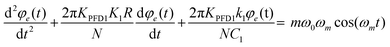
We consider a PLL with an FM input signal:
| | ωREF(t) = ω0 + mω0![[thin space (1/6-em)]](https://www.rsc.org/images/entities/char_2009.gif) sin(ωmt) sin(ωmt) | (1) |
where
ωm is the modulation angular frequency,
ω0 is the mean reference angular frequency, and
m is the modulation index. We define the phase error at the phase frequency detector (PFD) input by:
| | | φe(t) = φREF(t) − φ(t) | (2) |
Its first derivative is given by:
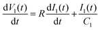
| |  | (3) |
Substituting
(1) in
(3) we obtain the second derivative given by:
| |  | (4) |
This equation will be useful to eliminate
φ(
t) from the differential equation describing the dynamics of the demodulator architecture.
In the following, we consider a linear, time-invariant continuous-time model (CTM) to keep the analysis of the FM-induced phase error simple. Describing the governing equations of the other blocks in the demodulator architecture is necessary in order to derive the output voltage of the demodulator. Considering Ccoarse tending to infinity, the PLL corresponds to a single-loop operation, as far as the small signal behaviour is considered. The gain of the PFD is defined as:
| |  | (5) |
where
Icp1 is the charge pump (CP) current in the fine tuning loop containing
C1 in the ON state. The average CP current is obtained as:
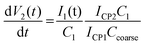
The resulting voltage across the
R–
C1 filter in the fine tuning loop is given as:
| |  | (7) |
Here, we used the first-order loop filter composed of C1 and R in order to simplify the analysis. A more detailed analysis would include the biasing resistors and bypass capacitors. However, the simplification does not imply loss of generality in the derived equation. The derivative of (7) is obtained as:
| |  | (8) |
The equation governing the oscillator output is given as:
| | 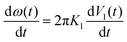 | (9) |
where
K1 is the oscillator gain. Substituting
(8) into
(9) we obtain:
| |  | (10) |
The PFD input phase obeys:
| |  | (11) |
Substituting
(10) into
(11) we obtain:
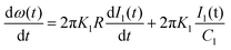
| |  | (12) |
Replacing the average value of
I1(
t) obtained in
(6) into
(12) we obtain:
| |  | (13) |
φ(
t) can be eliminated from the above equation by utilising
(4), resulting in:
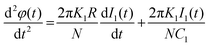
| |  | (14) |
Now we incorporate the coarse tuning loop Ccoarse in the analysis. According to the block diagram of the demodulator architecture shown in Fig. 4, there is no additional resistor as was present in the fine tuning loop. Therefore, the obtained voltage equation at the coarse tuning node corresponding to eqn (8) is:
| |  | (15) |
It can be seen from the demodulator architecture that the two charge pumps are driven by the same PFD, such that the waveforms V1(t) and V2(t) are the same, except for the constant factor given by the ratio of the charge pump currents in the ON state. Therefore, the voltage equation at the coarse tuning loop is given as:
| |  | (16) |
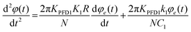
The oscillator frequency is the sum of the control voltages weighted by the gains of the oscillator for individual loops:
| |  | (17) |
Including the above constraints of two loops, we obtain a similar equation as
(13), and this is given as:
| |  | (18) |
where we introduced the following abbreviations:
| |  | (19) |
| |  | (20) |
Eqn (18) is a well-known differential equation describing a damped harmonic oscillator driven by external force.24 In our case, the driving force is the variation of the capacitance due to the flow of particles on top of the sensor. The solution of such a differential equation has been well discussed and can be used further to obtain the demodulator output voltage, which serves as the output of our sensor system.
The solution of the differential equation yields:
| | | V1(t) = Vdem cos(ωmt + φ1) | (22) |
The solution for
Vdem shows that it can be expressed as:
| |  | (23) |
The Vdem output is fed to the operational amplifier as shown in Fig. 5. A resistance Rin value of 5 MΩ was used and the corresponding RC biasing of the referenced input results in the same DC values of both the inputs to the amplifier. The Vdem output serves as one of the inputs to the amplifier, while the other input is the time averaged value of Vdem due to a very large biasing capacitance used.
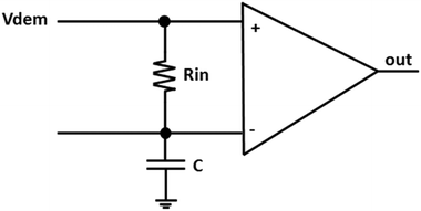 |
| | Fig. 5 Differential operational amplifier with RC biasing for self-calibration. | |
This technique eases the amplification of very small signal changes at the demodulator output regardless of PVT variations. It requires no further external calibration, which is often needed for differential amplifiers. This depicts the self-calibrating feature of the sensor architecture.
Fabrication of the prototype sensor system
The sensor system was fabricated in standard 0.13 μm SiGe:C BiCMOS technology of IHP microelectronics.25Fig. 6 shows the BiCMOS back-end of line (BEOL) stack with seven metal layers (five thin metal layers and two top thick metal layers). It should be noted here that the sensor IDE is on the top-most metal layer (TM2) of the BiCMOS stack. The TM2 metal layer has a thickness of 2 μm and is less resistive as compared to the thinner lower metal layers. This renders a high quality factor of the sensor and the overall resonator when combined with the on-chip inductors (also on TM2). The choice of metal layer is also suited for future polymer based microfluidic integration,18 rendering the sensor close to the analyte sample.
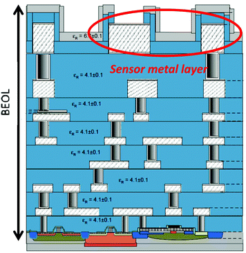 |
| | Fig. 6 Standard 0.13 μm BiCMOS stack of IHP with seven metal layers. | |
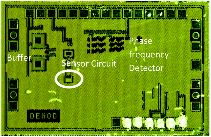
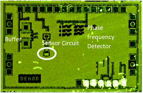
There is an additional passivation of Si3N4 of 300 nm on top of TM2 to separate the circuit from the external environment. The fabricated sensor chip photograph is shown in Fig. 7. The total area of the chip is 2.4 mm2.
 |
| | Fig. 7 Chip photograph of the sensor and demodulator architecture. | |
Results and discussion
The chip is glued on a printed circuit board made out of FR4 and wire bonding technique is used to make electrical connections to the bond pads. The total package size is 5 cm × 2 cm. With no requirement of any further reference electrodes or bulky calibration test-benches for measurements, the small size of the packaged chip is suitable for lab-on-chip applications. The fastest frequency modulation rate that can be detected by the sensor system determines the fluid pressure or velocity that can be used with such a sensor system. As was mentioned above, in the long channel approximation the mean particle velocity is equal to the mean fluid velocity. The limiting speed is defined by the settling time of the PLL. It is intuitive that the smaller the PLL settling time, the higher is the velocity of the fluid system that can be used. The settling time of the PLL is determined by the Ccoarse value.
Fig. 8 shows the simulated settling time of the PLL as a function of Ccoarse. It is seen that a value of 10 nF gives a settling time of approximately 3 μs. However, integration of an on-chip capacitor of 10 nF is physically impossible. Therefore, external capacitors have been integrated on-board to obtain such high capacitor values. The on-board capacitor integration enables the chip with a unique feature, where the settling time of the system can be adjusted based on the fluid velocity used in the system. This makes the chip suitable for a wide range of applications requiring different fluid velocities in the microfluidic system. In the present analysis, the settling time of the PLL shows the minimum required measurement time of the system could be as low as 3 μs to 5 μs. Therefore, extremely fast measurements can be performed.
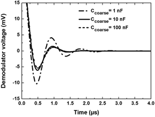 |
| | Fig. 8 The simulated settling time of the PLL as a function of the coarse loop filter capacitance. The settling time obtained is 3 μs. Capacitance change every 3 μs can be accurately detected. | |
Fig. 9 shows the simulated demodulator output voltage for a sinusoidal frequency modulation. The modulation period is 100 μs and the modulation index is 0.0001 (100 parts per million). From the particle flow modelling aspect, these simulation conditions translate to capacitance change due to particle flow every 100 μs. Such a dynamic rate of capacitance change can be related to extremely low solute or particle concentration in a solution. The modulation index relates to the change in resonant frequency of the oscillator due to the presence of a particle on top of the embedded IDE sensor. With the closed loop operating frequency of 14.3 GHz, the modulation index of 0.0001 translates to a change of 1.43 MHz. Therefore, the sensor shows a high order of sensitivity and detection resolution along with a very fast response time.
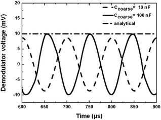 |
| | Fig. 9 The simulated demodulator output for an input modulating voltage of period 100 μs. The period of the voltage being much higher than the settling time of PLL, it is accurately followed by the demodulator. | |
As seen from the simulation results, the demodulator output voltage follows the modulating voltage. This can be attributed to the fact that the modulation period is much slower compared to the PLL settling time and, therefore, any modulation of the frequency due to capacitance change is accurately followed.
The electrical measurement of the chip shows that the overall DC current drawn by the chip from a 3.3 V supply is 80 mA. A measurement of the process variation was conducted to deduce the reproducibility of the chip. Several chips were measured from the same wafer and the output characteristics were not seen to vary more than 0.2%. The resonant oscillator circuit was characterized and measured to determine the operating frequency of the sensor. Fig. 10 shows the output spectrum of the closed loop resonant oscillator circuit.
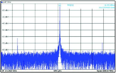 |
| | Fig. 10 The output spectrum of the sensor oscillator. The operating frequency is 14.272 GHz. | |
The tuning range of the PLL is from 12.6 GHz to 14.3 GHz, as was measured by tuning the bias voltage of the on chip Ccoarse varactor. The output power is −6.7 dBm and the reference spur level is below −62 dBm.
From the output spectrum shown in Fig. 10, the noise level compared to the signal output is shown; this noise floor is low enough to allow locking of the PLL. Additionally, high order low pass filter is employed for a smooth detector output at a given detector gain. As mentioned in the previous sections, in order to determine the sensitivity of the demodulator independently of a fluidic system, a small sinusoidal signal Vmod was applied to the modulating capacitor. The output voltage of the demodulator is taken as mentioned in the block diagram of the demodulator architecture and is fed to an operational amplifier for further amplification. The modulation input of the VCO has a gain of 100 MHz V−1 at a DC level of 1.25 V. By adding a sinusoidal low-frequency modulation signal of 10 mV peak to peak amplitude to a DC voltage of 1.25 V, the oscillator frequency changes by 1 MHz in open loop condition. This change of 1 MHz translates to a modulation index of 0.00007 or 70 parts per million. In the closed-loop operation, the oscillator frequency is kept constant, while the fine tuning voltage is modulated. By changing the modulation frequency and measuring the rms value of the demodulator output voltage, the demodulation sensitivity is obtained.
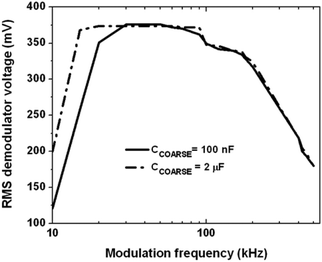
Fig. 11 shows the demodulator output as the function of the period of modulation. The applied DC voltage is 10 mV peak to peak. At modulation frequencies above the loop bandwidth of 300 kHz (time period ∼3 μs), the PLL cannot follow the modulating signal, and the demodulator output voltage is reduced. In terms of the sensing aspect, a modulating frequency of 300 kHz relates to a measurement speed of 3 μs. This shows that following the fluidic integration, every 3 μs a capacitance change due to the flow of particles on top of the senor can be accurately detected. This is a sufficiently fast measurement time, when compared to the state of the art particle sensing. The proposed architecture can, therefore, sufficiently increase the time efficiency of such microelectronics integrated fluidic systems. In order to detect changes in a slower fluid flow, where the change is of the order of milliseconds, a higher coarse tuning filter capacitor Ccoarse is required. The lower limit for the Ccoarse value of 100 nF is 50 kHz, corresponding to 20 μs. This lower limit can be further increased as seen in Fig. 11, where the Ccoarse value of 2 μF extends the lower limit of measurement to 20 kHz. This accounts for a measurement speed where a change of capacitance up to every 50 μs can be detected. Therefore, the sensor has a reconfigurable feature based on the on-board capacitors used.
 |
| | Fig. 11 Demodulator output voltage as a function of the modulation period. The demodulator voltage follows the input period till 300 kHz (3.3 μs). | |
The electrical characterization of the sensor shows that the sensitivity of the sensor is of the order of 70 to 100 ppm. For the closed loop operation at 14.3 GHz, this resolution translates to the detection limit of 1.43 MHz. For the modulating capacitor used in this work, this renders a change of 60 aF for initial capacitance value of 18 fF. From the aspect of frequency shift with respect to permittivity ambient of the IDE, this ultra- low modulation index detection capability shows a change of 0.25 in the absolute permittivity value in the dielectric ambient of the IDE, as measured in our previous work.18 Such high sensitivity and resolution makes the sensor system lucrative for a fluidic system with extremely low solute concentration and they are considerably higher than those of the established capacitive sensors.26,27 The capacitive detection technique is also independent of the polarity of the particles in the fluidic system.18 This is primarily due to the sensing principle being based on the dielectric contrast between the particles and the suspending medium. Therefore, the sensor system can be ideally used for charged and uncharged species. As mentioned previously, the measurement with the modulating capacitor is analogous to the capacitance modulation caused by the particle flow in a fluidic system. Therefore, the above measurements show that the established model is highly suitable for particle detection in fluidic systems. Another important aspect of lab-on-chip systems is their feasibility outside laboratory conditions,28–30 where the difficulty stems from external conditions, like temperature variations, mechanical stress etc. The working of the established prototype sensor system in such conditions will be dependent on the packaging. However, the external conditions will have a negligible influence on the sensing concept due to the on-chip stabilisation and configuration capabilities of the chip. In the subsequent sections the capability of correlation technique to eliminate the external noise is also shown. Therefore, the sensor system can be ideally used outside laboratory conditions as well. The sensor enhances the measurement time and also possesses a self-calibrating and reconfigurable feature, which can be utilized for different applications based on different fluid flow rates. The stability of the sensor circuit is obtained by the voltage divider at the charge pump output. This keeps the oscillator gain and the detector gain constant with respect to PVT variations.22
Proposed dual demodulator architecture
Elimination of noise by time-averaging
The noise in the system can limit the accuracy of the particle counting process. In order to improve the resolution, a long-term measurement with time averaging is a possible solution. For this modelling purpose, we consider two demodulator detectors with sensors located at different positions of a stream line in a fluidic channel. For simplicity, we assume that the momentary frequencies of the free-running sensor embedded oscillators represent a chain of rectangular pulses with random position. The corresponding demodulator outputs are shown in Fig. 12.
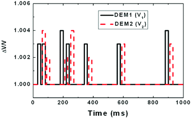 |
| | Fig. 12 Pulse train emulating the signals from 2 VCOs which are delayed by time Δt. | |
The demodulator output has the same waveform as the frequency output from the oscillators, since the PLL settling is fast compared to the frequency modulation. It can be calculated by multiplying the frequency change with the FM detector gain.
The cross-correlation between the two detector output voltages is defined by:
| | | C(t,τ) = 〈V2(t + τ)V1(t)〉 | (24) |
where the brackets denote the stochastic average. In steady state, the stochastic average can be calculated by time averaging over a long period of time
Tmax:
| | 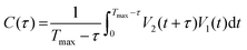 | (25) |
If the time is sampled with the step width
Ts, we can define:
| | | tn = nTs, n = 0,1,2…N | (26) |
and
| | | τm = mTs, m = 0,1,2…M | (27) |
The cross-correlation is then given by:
| |  | (28) |
For the chain of pulses depicted in Fig. 12, the cross-correlation is given in Fig. 13.
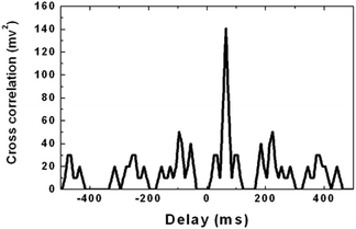 |
| | Fig. 13 Correlation between the two demodulator voltage outputs. | |
The peak maximum of the triangle gives the variance of the voltage, and the peak position gives the delay between the two detectors. The main advantage of the correlation method is the fact that non-correlated noise voltages v1 and v2 added to the ideal detector outputs V1 and V2 will be eliminated, provided that the number N of data points is sufficiently large.
In order to illustrate the noise reduction capability, we added strong random noise to the demodulator output signals. A correlation between the two pulse sequences infested with random noise signals demonstrates the elimination of the non-correlated noise shown in Fig. 14.
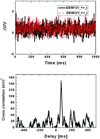 |
| | Fig. 14 Pulse trains showing frequency pulses from two oscillators covered with random noise (top). Cross correlation between the pulses (bottom). | |
As is evident from Fig. 14, non-correlated noise voltages on the two detector outputs can largely be eliminated by time averaging. This type of noise results from device noise in the two demodulators, both thermal noise and 1/f noise.
Another type of noise in silicon chips is supply and substrate noise.31 This type of noise may result in strongly correlated noise in the two demodulators, especially if they are integrated on the same chip. Since correlated noise will not be eliminated by time averaging, noise coupling between the demodulators through supply or substrate should be minimized. As discussed in ref. 32, this entails separate biasing of the critical blocks, sufficient distance between noise aggressors and noise victims, and the use of guard bands around critical circuit blocks. Moreover, electromagnetic coupling through close and parallel bond wires must be avoided. Another type of environmental noise is temperature noise. This type of noise was discussed in the context of oscillator-based reactance sensors,33 where environmental noise was reduced by noise cancellation and filtering. Since temperature changes are correlated noise sources for the two sensor capacitances, our approach cannot eliminate this type of noise. However, if the temperature changes are much slower than the total measurement time, they have a small effect on the demodulator sensitivity. Moreover, bandgap references for each of the two demodulators can be used to stabilize the supply voltages with respect to temperature variations.
Measurement technique for particle concentration and flow rate
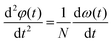
In order to detect the concentration of particles and flow rate in the laminar flow system using the two demodulator architecture, the dynamics of the individual demodulator has to be optimized while V1(t) in Fig. 4 is the individual demodulator output signal. The two tuning loops of the demodulator comprised of Ccoarse and Cfine have time constants τcoarse and τfine, respectively. τcoarse determines the sensitivity of the detector system and has to be considerably large compared to the delay between the “frequency change” events at the two oscillators due to the flow of particles on top of the respective sensors.Δt is the delay between the sensors. From the demodulator architecture shown in Fig. 4, and analysis of dual loop PLL,31 it is known that a frequency variation of the oscillator is restored by the coarse tuning loop and the time constant is given by:| | 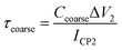 | (30) |
where ΔV2 is the voltage change on the coarse tuning loop due to frequency modulation as shown in Fig. 4. ICP2, which has been described above, is the charge pump current. The condition mentioned in (29) for highly sensitive architecture, that it requires a high value of τcoarse, can be achieved by lowering the ICP2 in conjunction with a high Ccoarse. In the case where the τcoarse is smaller than Δt, V2(t) in Fig. 4 can be taken as the output of the individual demodulator. Such a condition arises for extremely slow flow rate or very low solute concentration, which causes the “frequency change” event at the two oscillators to be widely spaced. Similar mathematics done for V2(t) as was done for V1(t) would show a loss of sensitivity in such a situation. However, V2(t) can be used as an output by sacrificing the sensitivity, as the delay is very large and the output voltage pulses are far apart from each other. In that case the Ccoarse value should be small for fast settling of V2(t). Thus, a self-calibration for different flow rates is seen in the dual demodulator approach as well.
In order to obtain the concentration of particles in the suspension we assume that the frequency pulses obtained from the two sensors are proportional to the particle density. This assumption is valid for low to medium solute concentration in the suspension, which is typically the case in fluidic systems. As mentioned in a previous section the temperature and process variation have minimum influence on our demodulator architecture, which implies that the output voltage of the two demodulator sensors is only proportional to the frequency changes in the oscillator. Therefore, the concentration of particles in the solution can be obtained from the cross-correlation of the two output signals and can be given as:
where
σv is the magnitude of the correlation peak and
α is a proportionality constant.
From the analysis it is seen that there is no theoretical limitation of particle concentration detection, as the correlation peak will grow with time. Therefore, any concentration of solute in a suspension can be estimated. However, if the measurement conditions (for e.g. temperature) change during the measurement time, detection of the real concentration can be affected and such a condition can be avoided using bandgap references as mentioned above.
The delay time of the correlation peak can be used to obtain the flow rate of the particles. If the sensors are separated by a distance s and the peak of the correlation occurs at Δt, the flow rate can be written as:
| |  | (32) |
In order to detect particles with different dielectric characteristics the voltage pulses would be used. For particles with different dielectric permittivity the height of the output voltage pulse will be different for different particles as is shown in Fig. 12. In order to detect the concentration of different particles in the suspension the height of the voltage pulses should be analysed. However, this requires time recording of the output pulses, which in turn would require excessive data processing and increase the complexity and area of the chip.
Conclusion
We have presented a highly sensitive PLL demodulator architecture in conjunction with a capacitance based frequency shift sensor for detection of dynamic capacitance change. The sensor system can be employed towards particle counting in a flow assisted fluid system. A sensitivity of 70 ppm was experimentally measured using a modulating capacitor. This sensitivity allows a sensing capability of 1 MHz frequency shift for a 14.3 GHz oscillator sensor. From the frequency shift sensor aspect this translates to the detection capability of 0.25 in the absolute permittivity value. Therefore, in the context of flow based sensors with a very low concentration of particles in the suspension this technique offers extremely high sensitivity. The second significant property of the sensor is its self-calibration capability based on the fluid flow rate. Capacitance change as fast as every 3 μs can be accurately detected by the sensor system and has been shown. The fast measurement approach reduces the measurement time considerably. Owing to the high operating frequency of the sensor, low-frequency dispersion mechanisms can be avoided while utilising the sensor for biological suspensions. On the other hand, the sensor has a very low-frequency (few kHz) output making the handling of the sensor highly simple. A configuration of two such detectors in a stream of particles in a microfluidic channel is proposed, where the system noise is suppressed by time averaging. After calibration, this method will provide particle density, mean velocity and fluid flow rate for a laminar flow in a microfluidic device.
Acknowledgements
The authors would like to thank the technology department of IHP microelectronics for fabrication of the chip.
Notes and references
- J. Daniels and N. Pourmand, Electroanalysis, 2007, 19(12), 1239–1257 CrossRef CAS PubMed.
- X. Luo and J. Davis, Chem. Soc. Rev., 2013, 42, 5944–5962 RSC.
- H. Mukundan, A. S. Anderson, W. Kevin Grace, K. Grace, N. Hartman, J. S. Martinez and B. I. Swanson, Sensors, 2009, 9, 5783–5809 CrossRef CAS PubMed.
- H. Ben-Yoav, T. E. Winkler, E. Kim, S. E. Chocron, D. L. Kelly, G. F. Payne and R. Ghodssi, Electrochim. Acta, 2014, 130, 497–503 CrossRef CAS PubMed.
- S. Kang, A. Nieuwenhuis, K. Mathwig, D. Mampallil and S. G. Lemay, ACS Nano, 2013, 7, 10931–10937 CrossRef CAS PubMed.
- E. E. Krommenhoek, J. G. E. Gardeniers, J. G. Bomer, A. Van den Berg, X. Li, M. Ottens, L. A. M. Van der Wielen, G. W. K. Van Dedem, M. Van Leeuwen, W. M. Van Gulik and J. J. Heijnen, Sens. Actuators, B, 2006, 115, 384–389 CrossRef CAS PubMed.
- K. Grenier, D. Dubuc, T. Chen, F. Artis, T. Chretiennot, M. Poupot and J.-J. Fournié, IEEE-TMTT, 2013, 61(4), 2012–2030 Search PubMed.
-
S. Guha, F. I. Jamal, K. Schmalz, C. Wenger and C. Meliani, IEEE-MTTS International Microwave Symposium (IMS 2014), 2014, Tampa, Florida, USA Search PubMed.
- Y. Yang, H. Zhang, J. Zhu, G. Wang, T.-R. Tzeng, X. Xuan, K. Huang and P. Wang, Lab Chip, 2010, 10, 553–555 RSC.
- G. A. Ferrier, S. F. Romanuik, D. J. Thomson, G. E. Bridges and M. R. Freeman, Lab Chip, 2009, 9, 3406–3412 RSC.
- K. Asami, E. Gheorghiu and T. Yonezawa, Biophys. J., 1999, 76, 3345–3348 CrossRef CAS.
- P. S. Singh, E. Katelhon, K. Mathwig, B. Wolfrum and S. G. Lemay, ACS Nano, 2012, 6, 9662–9671 CrossRef CAS PubMed.
- F. Aezinia and B. Bahreyni, IEEE Trans. Circ. Syst.-II, 2013, 60(11), 766–770 Search PubMed.
-
G. Nabovati, E. Ghafar-Zadeh, M. Mirzaei, G. Ayala-Charca, F. Awwad and M. Sawan, Proceedings IEEE International Symposium on Circuits and Systems, 2014, Melbourne, Australia Search PubMed.
- H. Lee, Y. Liu, R. M. Westervelt and D. Ham, IEEE J. Solid-State Circuits, 2006, 41(6), 1471–1480 CrossRef.
-
M. Kaynak, M. Wietstruck, C. Kaynak, S. Marschmeyer, P. Kulse, K. Schulz, H. Silz, A. Krueger, R. Bath, K. Schmalz, G. Gastrock and B. Tillack, Proceedings, IEEE-MTTS International Microwave Symposium (IMS 2014), Tampa, Florida, USA Search PubMed.
-
S. Guha, K. Schmalz, C. Wenger and C. Meliani, Proceedings European Microwave Conference (EUMC 2013), Nuremberg, Germany Search PubMed.
-
S. Guha, A. Wolf, M. Lisker, A. Trusch, C. Meliani and C. Wenger, Proceedings BIODEVICES, 2015, Lisbon, Portugal Search PubMed.
- F. Petersson, L. Aberg, A. Sward-Nilsson and T. Laurell, Anal. Chem., 2007, 79, 5117–5123 CrossRef CAS PubMed.
- J. Shi, H. Huang, Z. Stratton, Y. Huang and T. J. Huang, Lab Chip, 2009, 9, 3354–3359 RSC.
-
B. Razavi, RF Microelectronics, Prentice Hall, 2011 Search PubMed.
- K. Hu, S. A. Osmany, J. C. Scheytt and F. Herzel, Analog Integrat. Circuits Signal Process., 2011, 67(3), 319–330 CrossRef.
- F. Herzel, S. A. Osmany and J. C. Scheytt, IEEE Trans. on Circuits and Systems 1: Regular Papers, 2010, 57(8), 1914–1924 CrossRef.
-
R. P. Feynman, R. B. Leighton and M. Sands, The Feynman Lectures on Physics, Addison-Wesley, Reading, MA, 1964 Search PubMed.
- H. Ruecker,
et al.
, IEEE Electronic Devices Meeting (IEDM), 2007, 651–654 CAS.
- O. Elhadidy, M. Elkholy, A. Helmy, S. Palermo and K. Entesari, IEEE Trans. Microwave Theory Tech, 2013, 61(9), 3402–3416 CrossRef.
- G. Ferrier, S. Romanuik, D. Thomson, G. Bridges and M. Freeman, Lab Chip, 2009, 9, 3406–3412 RSC.
- G. Konvalina and H. Haick, Acc. Chem. Res., 2014, 47, 66–76 CrossRef CAS PubMed.
- H. Haick, Y. Broza, P. Mochalski, V. Ruzsanyi and A. Amann, Chem. Soc. Rev., 2014, 43, 1423–1449 RSC.
- M. Segev-Bar and H. Haick, ACS Nano, 2013, 7(10), 8366–8378 CrossRef CAS PubMed.
- F. Herzel and B. Razavi, IEEE Transactions on Circuits Systems II: Analog Digit. Signal Processing, 1999, 46(1), 56–62 CrossRef.
- S. A. Osmany, F. Herzel and J. C. Scheytt, Analog Integr. Circuits Signal Process., 2013, 74, 545–556 CrossRef PubMed.
- H. Wang, C. C. Weng and A. Hajimiri, IEEETrans. Microwave Theory Tech., 2013, 61, 2215–2229 CrossRef.
|
| This journal is © The Royal Society of Chemistry 2015 |

 Open Access Article
 This Open Access Article is licensed under a