 Open Access Article
 This Open Access Article is licensed under a
 Creative Commons Attribution 3.0 Unported Licence
Multiband photoluminescence from carbon nanoflakes synthesized by hot filament CVD: towards solid-state white light sources
B. B.
Wang
a,
K.
Ostrikov
*bc,
K.
Zheng
d,
L.
Wang
d and
S. S.
Zou
a
aCollege of Chemistry and Chemical Engineering, Chongqing University of Technology, 69 Hongguang Rd, Lijiatuo, Banan District, Chongqing 400054, P. R. China
bPlasma Nanoscience Centre Australia (PNCA), CSIRO Materials Science and Engineering, P. O. Box 218, Lindfield, NSW 2070, Australia. E-mail: Kostya.Ostrikov@csiro.au
cPlasma Nanoscience, School of Physics, The University of Sydney, Sydney, NSW 2006, Australia
dInstitute of Microstructure and Properties of Advanced Materials, Beijing University of Technology, Beijing 100124, P. R. China
First published on 30th January 2014
Abstract
Carbon nanoflakes (CNFLs) are synthesized on silicon substrates deposited with carbon islands in a methane environment using hot filament chemical vapor deposition. The structure and composition of the CNFLs are studied using field emission scanning electron microscopy, high-resolution transmission electron microscopy, micro-Raman spectroscopy, and X-ray photoelectron spectroscopy. The results indicate that the CNFLs are composed of multilayer graphitic sheets and the area and thickness of CNFs increase with the growth time. The photoluminescence (PL) of CNFLs excited by a 325 nm He–Cd laser exhibits three strong bands centered at 408, 526, and 699 nm, which are related to the chemical radicals terminated on the CNFLs and the associated interband transitions. The PL results indicate that the CNFLs are promising as an advanced nano-carbon material capable of generating white light emission. These outcomes are significant to control the electronic structure of CNFLs and contribute to the development of next-generation solid-state white light emission devices.
Introduction
Solid-state lighting (SSL) is a rapidly developing technology where electric power is converted into optical emission. The SSL has the advantages of high luminosity, energy-efficiency, environmental friendliness, etc.1–3 These place SSL devices among the most promising next-generation light sources.1 White light can be obtained by combining blue, green and red emitters. However, significant energy losses and, consequently, a relatively low conversion efficiency are inevitable.4 This is why a great deal of effort has recently been devoted to the development of advanced white light-emitting nanomaterials.Existing examples of nanomaterials that directly emit white light include hybrid semiconductor materials such as 2D-[Cd2Se2(ba):Te] (ba = bultylamine),1 ZnO nanoparticles mixed with graphene,2 CdSe–ZnS core–shell nanocrystals hybridized with InGaN/GaN,5 and some others. However, white light emitting nanomaterials composed of a single chemical element remain quite rare. For example, nitrogen-doped carbon films and nanodots have been reported to directly generate white light.6,7 The generation of white light may be attributed to various interband transitions6 and size-dependent effects,7 which is particularly strong for carbon quantum dots (commonly termed C-dots). However, it is quite challenging to control the C-dot size which leads to limited tunability of the luminescence and quantum yield of photons.8
Graphene films composed of a single or a few atomic carbon layers are considered as other viable luminescent carbon nanomaterials. However, the zero bandgap of a perfect single-layer graphene sheet makes it difficult to generate photoluminescence (PL).9 On the other hand, graphene nanoflakes have a bandgap thereby showing semiconducting responses.10,11 Likewise, there are reports that graphene oxide with a bandgap can generate PL.12–14 One can thus expect effective generation of PL emission also from the carbon nanoflakes (CNFLs), which are of primary interest in this study.
Indeed, blue emission can be generated from the aromatic or olefinic functional groups,15 green emission is related to the bandgap,6 while red PL is associated with the defect states created by oxygen.12 Thus, the CNFLs can become the white light emitting materials if they are modified by the above functional groups. The hydrocarbon radicals formed from methane at high temperatures can form olefinic molecules.16,17 Simultaneously, the residual oxygen in the reaction chamber can react with the CNFLs to form some oxygen-defect states. Thus, the CNFLs formed in a methane environment can indeed be expected to generate white light emission. To satisfy these requirements, here we use the hot filament chemical vapor deposition (HFCVD) process to synthesize the white light emitting CNFLs.
Moreover, here we employ an unconventional growth mechanism which does not rely on commonly used metal catalysts.18 To control the CNFL growth, we use carbon islands as the seeds. These seeds are pre-deposited on the mirror-polished silicon substrates by the plasma-enhanced hot filament chemical vapor deposition (PEHFCVD) using a mixture of methane, hydrogen, and nitrogen gases. The carbon islands are then used in HFCVD synthesis of the CNFLs in a methane environment.
The room-temperature PL spectra show three strong PL bands centered about 408, 526 and 699 nm, which are different from the single PL band of graphene oxide.12–14 For the PL of graphene oxide, different PL mechanisms are suggested, which are related to the oxygen-defect states12 and the electron–hole pairs generated in the sp2 islands.13,14
In contrast, our CNFLs simultaneously generate three PL bands owing to the different mechanisms of photoluminescence. These PL properties are related to the morphological and structural features of the CNFLs and offer interesting opportunities for the development of next-generation white light luminescent devices.
Experimental details
Before the synthesis of carbon nanodots and CNFLs, the organic and inorganic residues on the surfaces of silicon substrates were removed by a chemical method. To remove the organic residues, the substrates were sequentially cleaned for 15 min in toluene, acetone, and ethanol ultrasonic baths, respectively. For removing the inorganic residues, the substrates were placed in a solution composed of NH3·H2O, H2O2 and H2O (with a volume ratio of 1![[thin space (1/6-em)]](https://www.rsc.org/images/entities/char_2009.gif) :2:5) and boiled at 75 °C for 15 min. Finally, they were washed several times with deionized water.
:2:5) and boiled at 75 °C for 15 min. Finally, they were washed several times with deionized water.
To synthesize the CNFLs, carbon nanodots were pre-deposited on the silicon substrates using PEHFCVD. Here, we used PEHFCVD to grow the carbon islands because low-temperature reactive plasmas are versatile in nanomaterial synthesis and processing.8 The PEHFCVD system is similar to the system described in detail elsewhere.19
In the CVD reactor, the reactive gases are decomposed into chemical radicals by hot tungsten filaments (∼1800 °C), and then the radicals are further ionized to generate positive ions by the plasma produced by a DC power supply. Because the nucleation of carbon on the mirror-polished silicon substrate can be improved by a negative bias,20 the anode and cathode are connected to the filaments and the substrate through a molybdenum holder. A short distance of ∼8 mm between the filaments and the substrate make the substrate heated to about 900 °C in a short time, which is measured by a thermocouple. When a base pressure lower than 2 Pa is reached in the CVD reactor, 20 sccm nitrogen and 80 sccm hydrogen are introduced into it and the pressure is adjusted to about 2 × 10³ Pa. The tungsten filaments are heated by an AC power supply.
Once the substrate is heated to about 900 °C, the DC power supply is turned on to produce the plasma. After the silicon substrate is treated for 5 min with N2 + H2 plasma, the DC power supply is turned off, and then methane is let into the CVD reactor while the flow rates of methane, nitrogen and hydrogen are adjusted to 20, 30, and 50 sccm, respectively. At the same time, the DC power supply is turned on again and the bias current is then set to 160 mA to deposit the carbon nanodots for 15 min.
The CNFLs are then synthesized in the HFCVD system, where the synthesis procedure is quite similar to the deposition of the carbon islands described above. After the CVD reactor is pumped down to a base pressure lower than 2 Pa, 50 sccm hydrogen is introduced into it and the pressure is adjusted to 2 × 10³ Pa. When the substrate temperature reaches about 930 °C, the hydrogen gas flow controller is turned off. Simultaneously, 50 sccm methane flow is quickly let into the CVD reactor to grow the CNFLs. In this series of experiments, three specimens A–C are prepared in the processes that lasted 4, 6, and 8 min, respectively.
The morphological features of the CNFLs are investigated using a Hitachi S-4800 field emission scanning electron microscope (FESEM) operated with 15 kV electron beam accelerating voltage. The chemical structure of the CNFLs is analyzed using a JEOL 2010F transmission electron microscope (TEM) operated at 200 kV. The composition of CNFLs is studied using a HR 800 micro-Raman spectrometer with a 532 nm line of a semiconductor laser as the excitation source, an ESCALAB 250 X-ray photoelectron spectrometer (XPS) using an Al Kα X-ray source, and an 8400S Shimadzu Fourier transform infrared (FTIR) spectrometer, respectively. The PL of CNFLs is measured using the HR 800 micro-Raman system, where a 325 nm line of a He–Cd laser was used as the excitation source; the power of the laser was set to 10 mW.
Results and discussion
Structure and composition of CNFLs
Fig. 1 shows the FESEM image and Raman spectrum of the carbon islands deposited on the silicon substrate. As shown in Fig. 1(a), the carbon islands are non-uniformly distributed on the silicon surface and their diameters are also non-uniform. According to the results obtained by standard digital image processing of the relevant SEM images, the diameter of the typical carbon islands is within the 10–80 nm range. Fig. 1(b) shows two Raman peaks at about 1373 and 1600 cm−1, which are the common D and G peaks of sp2 carbon nanomaterials, respectively.21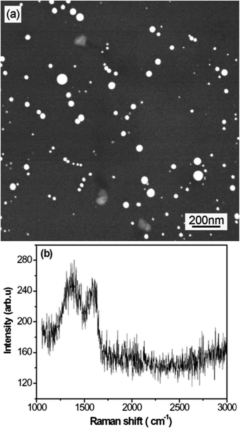 | ||
| Fig. 1 FESEM image (a) and Raman spectrum (b) of carbon islands deposited on a silicon substrate. | ||
Fig. 2 shows the FESEM images of specimens A–C. From Fig. 2, one can see that the area of CNFLs becomes larger from specimen A to specimen C, which indicates that the CNFLs increase in size with the growth time.
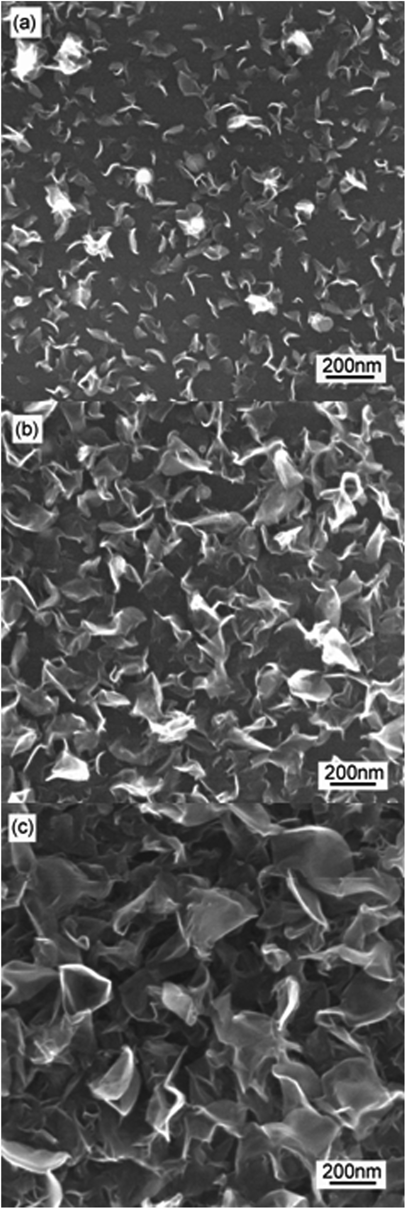 | ||
| Fig. 2 FESEM images of specimens A–C: (a) A; (b) B; (c) C. | ||
Fig. 3 presents the Raman spectra of specimens A–C, which show the D, G, and 2D peaks at about 1343, 1580, and 2696 cm−1, respectively. From Fig. 3, the intensity ratio of G to D peaks is about 1.2, 1.4 and 1.7, respectively, which means that the G peak is stronger than the D peak. The strong G and 2D peaks indicate that the CNFLs are composed of a few graphene sheets.22 The ratio of intensities of 2D and G peaks deduced from Fig. 3 is about 0.85, 0.82, and 0.65 for spectra (1)–(3), respectively. These data suggest that the CNFL thickness gradually increases with the growth time as evidenced by the lower ratio of the intensities of the 2D and G peaks as the number of graphene sheets becomes larger.23
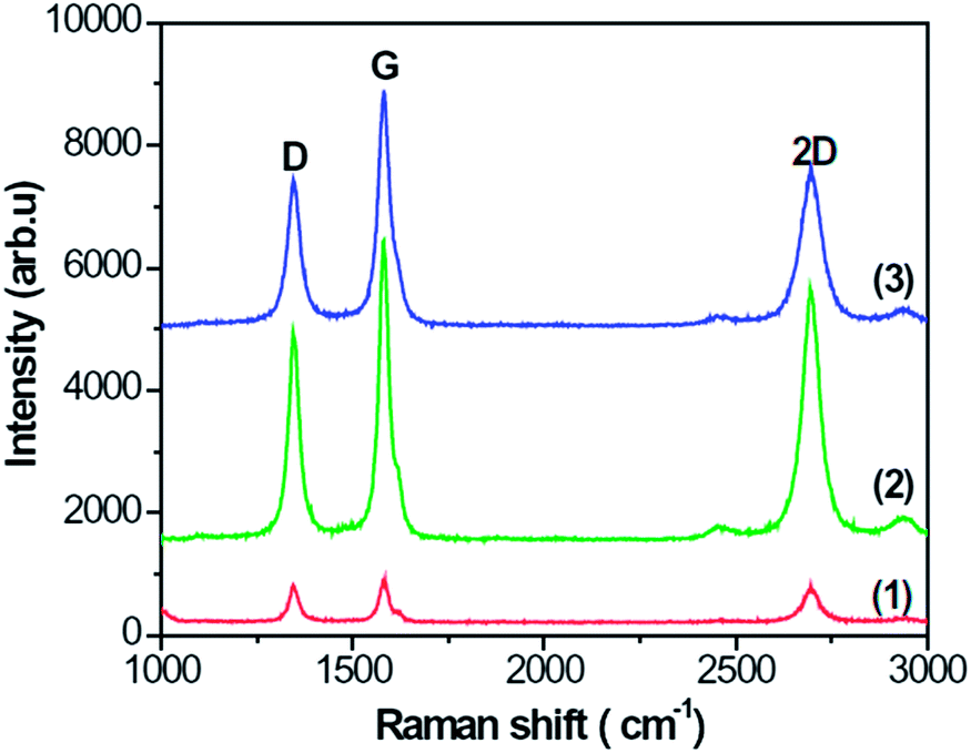 | ||
| Fig. 3 Raman spectra of specimens A–C: (1) A; (2) B; (3) C. | ||
Due to the similarity of Raman spectra of the specimens, specimen B was investigated by TEM after the CNFLs were scraped from the silicon substrate using a sharp knife and the results are shown in Fig. 4. From the high-resolution TEM image in Fig. 4(b), one can see regular graphitic sheets. We used Digital Micrograph software (Gatan™) to obtain the width of 10 carbon sheets and found it to be equal to 3.3 nm, giving a 0.33 nm spacing between two carbon sheets, which clearly corresponds to the interlayer spacing of graphite (0.335 nm).24 In Fig. 4(c), the fast Fourier transform (FFT) image shows two families of spots, which indicate that the CNFLs are composed of only a few graphene sheets.25 Simultaneously, Fig. 4(c) shows the weak diffusive rings, which most likely originated due to the presence of amorphous carbon on the microgrid used for holding the TEM specimen. A quite similar pattern has previously been reported for multilayer graphene sheets.26
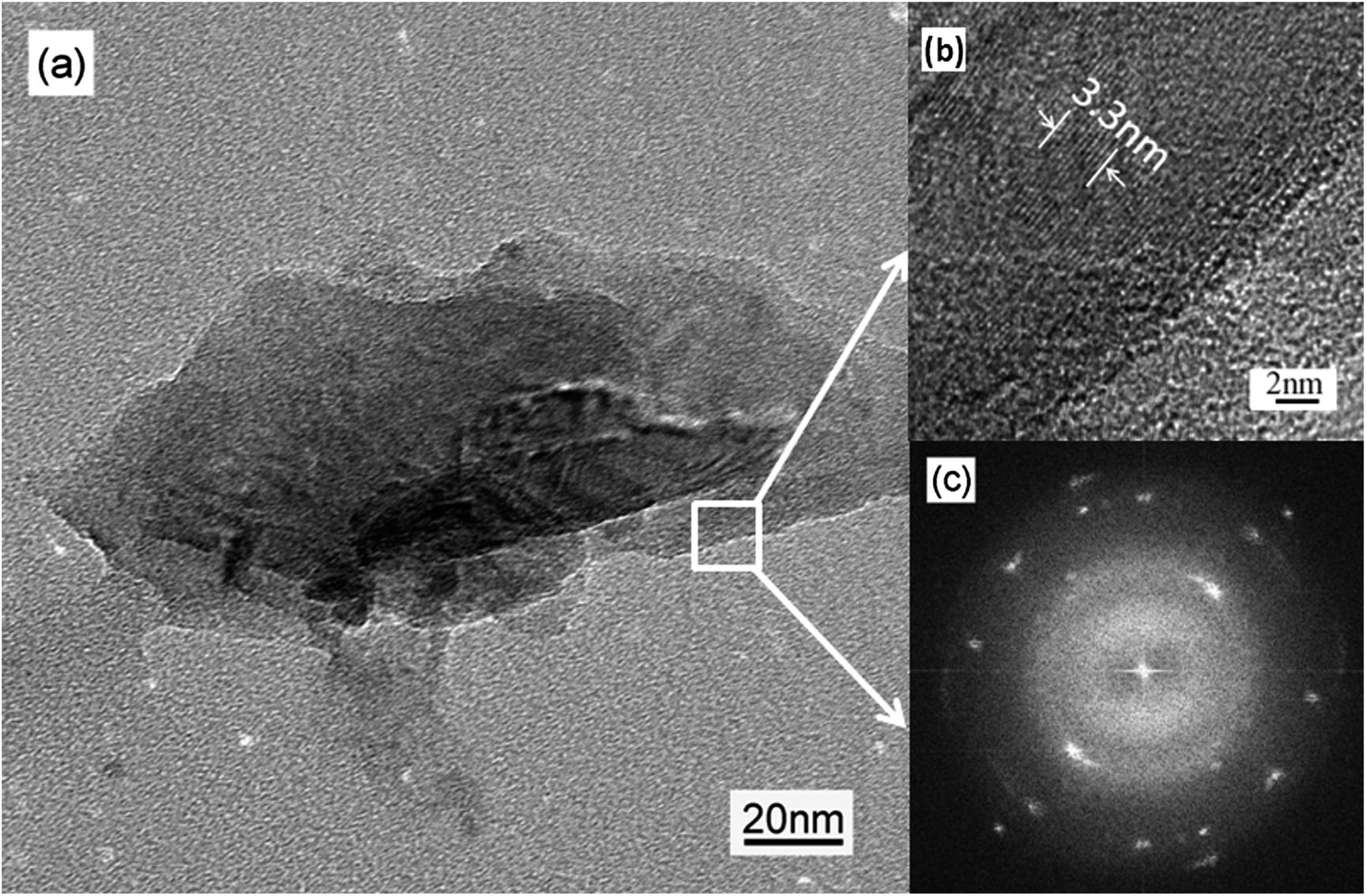 | ||
| Fig. 4 TEM and FFT images of specimen B: (a) TEM; (b) high-resolution TEM; (c) FFT image. | ||
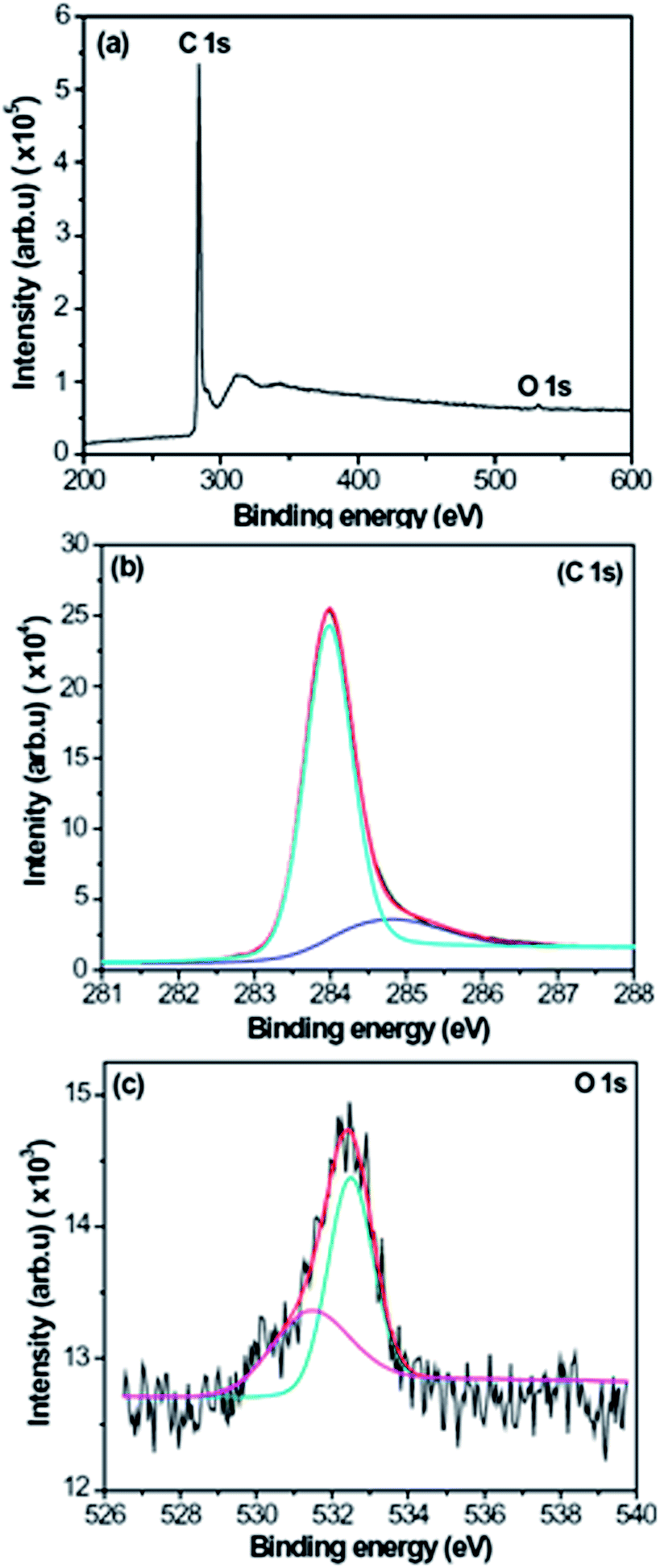
To further confirm the composition of CNFLs, specimen A was analyzed by XPS. Fig. 5 shows the XPS spectra of specimen A. The wide XPS spectrum in Fig. 5(a) shows the C 1s and O 1s XPS peaks at about 283.98 and 532.46 eV, respectively. The very weak peak at 532.46 eV implies that there is a very small amount of oxygen in the CNFLs, with an oxygen content of about 0.8 at% according to the XPS measurement results. Fig. 5(b) and (c) represent the C 1s and O 1s XPS spectra. For the analysis of bonding states of the elements, the C 1s and O 1s XPS spectra are fitted by the standard XPS fitting software after Shirley background subtraction. As shown in Fig. 5(b), the C 1s peak is fitted by two peaks at about 283.97 and 284.79 eV, which are attributed to the Si–C and sp2 C–C bonds, respectively.27,28 For the O 1s peak, it is decomposed into two peaks at about 531.44 and 532.46 eV, respectively. The peak at ∼531.44 eV is related to the C![[double bond, length as m-dash]](https://www.rsc.org/images/entities/char_e001.gif) O bond while the peak at ∼532.46 eV is associated with the C–O–H and/or C–O–C bonds.29
O bond while the peak at ∼532.46 eV is associated with the C–O–H and/or C–O–C bonds.29
 | ||
| Fig. 5 XPS spectra of specimen A: (a) XPS wide spectrum; (b) C 1s XPS spectrum; (c) O 1s XPS spectrum. | ||
In Fig. 5(b), one can see that the peak related to silicon carbide is stronger than the sp2 carbon peak, which is related to the formation of CNFLs from the carbon islands. The growth time of specimen A is the shortest among the three specimens, thus the area of CNFLs is small, which is confirmed by Fig. 2. When the hydrocarbon radicals are deposited on the silicon surface, they react with silicon to form silicon carbide. Due to the small area of CNFLs, most of the substrate surface contributes to the XPS measurement. As a result, the peak related to silicon carbide appears stronger than the sp2 carbon peak.
In the XPS spectra, the appearance of the carbon oxide peak results from the residual oxygen in the CVD reactor. During the growth of CNFLs, oxygen gas is not employed, thus the above peak originates from the residual gases in the CVD reactor. Because oxygen is an active element, it easily reacts with carbon to form carbon oxide. However, the residual oxygen content is small so that the peak related to oxygen is weak.
The XPS spectrum in Fig. 5(c) shows the peaks related to the CO, C–O–H, and C–O–C bonds. To further confirm the functional groups related to these bonds, specimen C was studied by FTIR and the results are shown in Fig. 6. In Fig. 6, the peak at about 624 cm−1 is assigned to out-of-plane C–H deformation vibrations,30 the peaks at 1382 and 1620 cm−1 are attributed to the C–O–C and CC groups, respectively,31 the peak at about 2345 cm−1 is related to the CO2 group,32 and the peaks at 3406–3555 cm−1 are associated with the presence of –OH groups.33
 | ||
| Fig. 6 FTIR spectrum of specimen C. | ||
Possible role of carbon islands in CNFL growth
Before the growth of CNFLs, we pre-deposit the carbon islands on the silicon surfaces to promote the formation of CNFLs. The pre-deposition of carbon islands plays two possible roles in the CNFL growth. One is the acceleration of the reactions among the hydrocarbon radicals because carbon black can be used to catalyze the decomposition of methane;34 the other is the lowering of the energy for carbon nucleation due to the formation of pit-like defects at the joints of the islands with the silicon surface.20During the synthesis of CNFLs, methane is decomposed into various hydrocarbon radicals by the hot filaments,35 with the initial products, methyl radicals and atomic hydrogen, forming via the following reaction,16
| CH4 → CH3 + H. | (1) |
Of course, methane cannot be completely decomposed by the hot filaments due to the continuous gas flow. When the hydrogen, methyl radicals, and methane molecules reach the silicon surface, methane reacts with hydrogen to form the methyl radical through the following reaction,16
| H + CH4 → CH3 + H2. | (2) |
On the silicon surface, the methyl radicals form ethylene molecules through a series of reactions,16 then ethylene molecules form benzene molecules,36 which in turn contribute to the CNFL formation. Because carbon black can accelerate the decomposition of methane, it can also accelerate the reaction of hydrocarbon radicals so that the CNFLs can be formed fast on the surfaces of carbon islands. One can thus say that the carbon islands promote the formation of CNFLs and this is the reason for the presence of more CNFLs near the carbon islands than elsewhere, as shown in Fig. 2(a).
Due to the carbon islands, the pit-like defects are formed at the joints of the carbon islands with the silicon surface. A recent study revealed that a lower energy is required for carbon nucleation in a pit relative to a plain surface.20 Thus, the nucleation of CNFLs requires a low energy at the joints of the islands with the silicon surface, i.e., the growth of CNFLs starts from the carbon islands. This is another reason that the carbon islands can indeed promote the formation of CNFLs.
Here we emphasize that the use of high concentration of methane as a carbon source for the carbon island synthesis was possible in this work, in part due to the ability of the hot-filament-produced plasma to effectively dissociate precursor molecules. In addition, the plasma can be used to grow a number of other nanomaterials such as various nanostructures including nanowires.37–40
It is also worth mentioning that our method of CNFL growth is quite simple because it is catalyst-free and no further treatment is required for the PL study. This is an obvious advantage compared to other studies,12,18 where a catalyst was deposited using a sputtering system while further oxygen plasma treatment was needed to prepare the specimens for the PL analysis.
PL properties of CNFLs
Fig. 7 shows the PL spectra of CNFLs obtained from different places on the surfaces of specimens A–C, which show three PL bands centered about 408, 526, and 699 nm, respectively. The same peak position for every corresponding band in Fig. 7(a) and (b) indicates that the PL emission is generated from the CNFLs. Previously, the PL properties of graphene-based nanomaterials were studied.12–14 Gokus et al. proposed that the PL generation of graphene oxide is related to the defect states induced by oxygen,12 while Eda and Luo et al. suggested that the PL in graphene is associated with the band emission from electron-confined sp2 carbon islands.13,14 However, Shen et al. attributed the strong PL emission of graphene quantum dots to the surface-passivation effects.41 In addition, a combination of graphene quantum dots with agar and zinc oxide quantum dots as the conversion materials helped converting blue emission into white light. The generation of blue light is attributed to the functional groups on the surfaces of graphene quantum dots and the electron transition between the O 2p state of zinc oxide quantum dots and the unoccupied state of graphene oxide, respectively.42,43 Guo and coworkers44 studied the photoinduced electron transfer between pyridine coated cadmium selenide quantum dots and single-sheet graphene and found that the single-sheet graphene can quench the emission of quantum dots.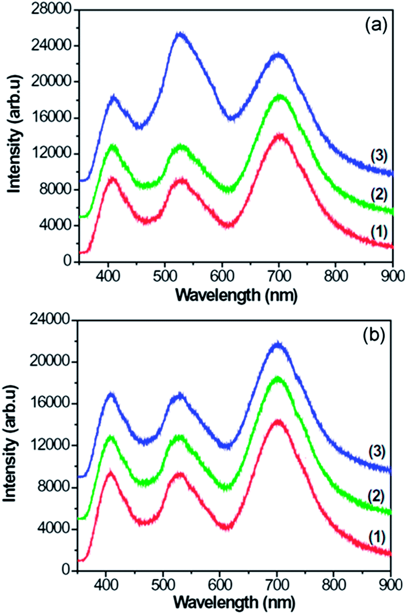 | ||
| Fig. 7 PL spectra of CNFLs obtained from different places on the specimen surfaces: (1) A; (2) B; (3) C. | ||
In these studies, the PL properties of monolayer graphene, graphene quantum dots or their hybrids were studied. In particular, a sole PL band was detected,12–14 implying that the mechanism of PL in our case may be quite different. Indeed, the simultaneous excitation of three PL bands suggests the co-existence of multiple mechanisms of photoluminescence in our CNFL samples.
For our specimens, the CNFLs are composed of multilayer graphene. If the PL generation is interpreted using the radiative recombination of electron–hole pairs produced in the sp2 clusters by photo-induction, the size of clusters should be about 1 nm.45 Since the thickness of CNFLs in Fig. 2 is about 8 nm, it is impossible to generate PL through radiative recombination of electron–hole pairs produced in the sp2 carbon clusters. Previous results suggest that the bandgap of ∼3 nm sp2 carbon clusters is about 0.5 eV, with the corresponding wavelength of 2480 nm.13 For the CNFLs in our specimens, the bandgap is lower than 0.5 eV because it is reduced with increase in the size of sp2 carbon clusters,13 thus it is unlikely to attribute our results to the bandgap emission.
The research results of Fanchini et al. indicate that the energy gap of π* and π states of carbon materials is ∼2.5 eV although their optical gap is lower than 1 eV.46 Other authors6 used the interband transition mechanism to explain the PL generation of carbon materials according to the state density model. In this model the PL bands above 2 eV originate from the transition between the π* and π bands, or the transition between the σ* band and the valence band formed by defects, while the transition between the π* band and the valence band formed by defects occurs in the energy range below 2 eV. The transition mechanism was also used to interpret the generation of multiple PL bands.43 Furthermore, the results of Chiou et al. indicate that the PL generation of graphene nanoflakes is related to the induced changes in the electronic structure and the presence of disorder-induced localized states in the region of π states and the gap between the π* and π states.47 In addition, the PL generation is related to the functional group and defects.12,15,42 These PL mechanisms will be used below to interpret the PL generation in our experiments.
From the above analyses, we note that hydrocarbon (e.g., methyl, and ethenyl) radicals can be formed during the growth of CNFLs. When the growth of CNFLs stops, these radicals can terminate the edges and also possibly the surfaces of the CNFLs because they are easily bonded to benzene.48 Because blue PL can be generated from the aromatic or olefinic molecules,15 the blue PL band centered about 408 nm is attributed to the ethenyl radicals on the CNFLs. The energies corresponding to 408, 526, and 699 nm are 3.05, 2.36 and 1.78 eV, respectively. The energy gap of π* and π states of carbon materials is ∼2.5 eV.46 According to the interband transition mechanism,6 the blue PL band can originate from the transition between σ* and π bands.
Fig. 2 also reveals that the CNFLs are morphologically and structurally similar to the vertical graphene sheets8,11 which also have a bandgap. Thus, the green PL band centered about 526 nm can indeed be attributed to the transition between the π* and π bands.6Fig. 5(c) and 6 indicate the formation of C–O bonds, i.e., there are defect states formed within the π* and π bands.12 The red PL band centered about 699 nm is related to the transition between the π* band and the oxygen-defect states.
Fig. 3 indicates that the CNFLs vary in thickness which in turn leads to bandgap variation among different structures. As a result, the intensity of PL bands also varies among the specimens and the measurement spots shown in Fig. 7. The PL efficiency trends are similar to the results of other authors.49
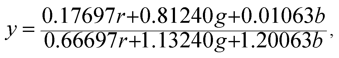
The Commission Internationale de L'eclairage (CIE) chromaticity coordinate diagram for white light emission is presented in Fig. 8. The CIE chromaticity coordinates of the specimens are calculated according to the following equations:51,52
 | (3) |
 | (4) |
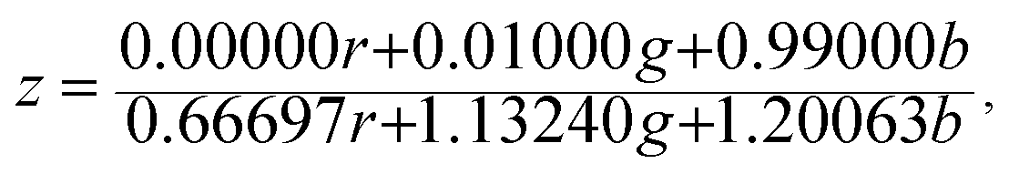 | (5) |
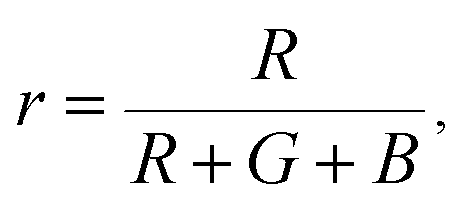 | (6) |
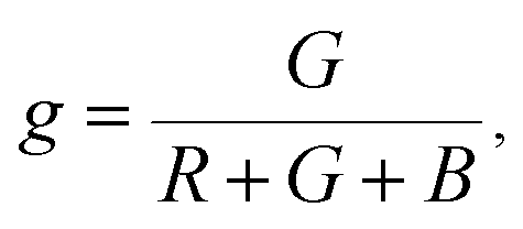 | (7) |
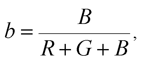 | (8) |
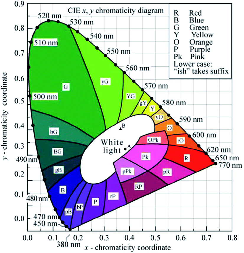 | ||
| Fig. 8 CIE 1931 x,y chromaticity diagram (reprinted with permission from ref. 50). | ||
Conclusion
In summary, CNFLs were synthesized on silicon substrates by HFCVD and their structure and composition were studied using FESEM, high-resolution TEM, micro-Raman spectroscopy, and XPS analyses. The results indicate that the area and thickness of CNFLs increase with the growth duration.The photoluminescence studies confirm that the CNFLs can generate three strong PL bands centered about 408, 526, and 699 nm. These bands are attributed to the chemical radicals terminated on the CNFs and the transitions between the σ* and π bands, between the π* and π bands, and between the π* band and the oxygen-defect states, respectively. The simultaneous generation of the blue, green and red photoluminescence bands indicates that the CNFLs can be regarded as effective sources of white light emission. These results advance our knowledge of the growth and optoelectronic properties of graphene-based materials and contribute to the development of next-generation solid-state white light emission devices.
Acknowledgements
This work is partially supported by the National Natural Science Foundation of China (11004004), the Beijing Municipal Natural Science Foundation (1112004), CSIRO's OCE Science Leadership Scheme, and the Australian Research Council.Notes and references
- W. Ki, J. Li, G. Eda and M. Chhowalla, J. Mater. Chem., 2010, 20, 10676 RSC.
- P. Kumar, L. S. Panchakarla, S. V. Bhat, U. Maitra, K. S. Subrahmanyam and C. N. R. Rao, Nanotechnology, 2010, 21, 385701 CrossRef PubMed.
- S. Ye, F. Xiao, Y. X. Pan, Y. Y. Ma and Q. Y. Zhang, Mater. Sci. Eng., R, 2010, 71, 1 CrossRef PubMed.
- A. H. Mueller, M. A. Petruska, M. Achermann, D. J. Werder, E. A. Akhadov, D. l. D. Koleske, M. A. Hoffbauer and V. I. Klimov, Nano Lett., 2005, 5, 1039 CrossRef CAS PubMed.
- S. Nizamoglu, T. Ozel, E. Sari and H. V. Demir, Nanotechnology, 2007, 18, 065709 CrossRef.
- Y. Iwano, T. Kittaka, H. Tabuchi, M. Soukawa, S. Kunitsugu, K. Takarabe and K. Itoh, Jpn. J. Appl. Phys., 2008, 47, 7842 CrossRef CAS.
- W. Kwon, S. Do, J. Lee, S. Hwang, J. K. Kim and S.-W. Rhee, Chem. Mater., 2013, 25, 1893 CrossRef CAS.
- K. Ostrikov, E. C. Neyts and M. Meyyappan, Adv. Phys., 2013, 62, 113 CrossRef CAS.
- L. Caro, M. J. Meziani, S. Sahu and Y. P. Sun, Acc. Chem. Res., 2013, 46, 171 CrossRef PubMed.
- M. Y. Han, B. Özyilmaz, Y. Zhang and P. Kim, Phys. Rev. Lett., 2007, 98, 206805 CrossRef.
- D. H. Seo, S. Kumar and K. Ostrikov, Carbon, 2011, 49, 4331 CrossRef CAS PubMed.
- T. Gokus, R. R. Nair, A. Bonetti, M. Böhmler, A. Lombardo, K. S. Novoselov, A. K. Geim, A. C. Ferrari and A. Hartschuh, ACS Nano, 2009, 3, 3963 CrossRef CAS PubMed.
- G. Eda, Y.-Y. Lin, C. Mattevi, H. Yamaguchi, H.-A. Chen, I.-S. Chen, C.-W. Chen and M. Chhowalla, Adv. Mater., 2010, 22, 505 CrossRef CAS PubMed.
- Z. Luo, P. M. Vora, E. J. Mele, A. T. C. Johnson and J. M. Kikkawa, Appl. Phys. Lett., 2009, 94, 111909 CrossRef PubMed.
- F. Bonaccorso, Z. Sun, T. Hasan and A. C. Ferrari, Nat. Photonics, 2010, 4, 611 CrossRef CAS.
- C.-J. Chen, M. H. Back and R. A. Back, Can. J. Chem., 1976, 54, 3175 CrossRef CAS.
- D. B. Murphy, R. W. Carroll and J. E. Klonowski, Carbon, 1997, 35, 1819 CrossRef CAS.
- Y. Wu, P. Qiao, T. Chong and Z. Shen, Adv. Mater., 2002, 14, 64 CrossRef CAS.
- B. B. Wang, Q. J. Cheng, X. X. Zhong, Y. Q. Wang, Y. A. Chen and K. Ostrikov, J. Appl. Phys., 2012, 111, 044317 CrossRef PubMed.
- B. B. Wang, W. L. Wang, K. J. Liao and J. L. Xiao, Phys. Rev. B: Condens. Matter Mater. Phys., 2001, 63, 085412 CrossRef.
- A. C. Ferrari and J. Robertson, Phys. Rev. B: Condens. Matter Mater. Phys., 2001, 64, 075414 CrossRef.
- A. C. Ferrari, J. C. Meyer, V. Scardaci, C. Casiraghi, M. Lazzeri, F. Mauri, S. Piscanec, D. Jiang, K. S. Novoselov, S. Roth and A. K. Geim, Phys. Rev. Lett., 2006, 97, 187401 CrossRef CAS.
- X. Li, W. Cai, J. An, S. Kim, J. Nah, D. Yang, R. Piner, A. Velamakanni, I. Jung, E. Tutuc, S. K. Banerjee, L. Colombo and R. S. Ruoff, Science, 2009, 324, 1312 CrossRef CAS PubMed.
- G. Srinivas, Y. Zhu, R. Piner, N. Skipper, M. Ellerby and R. Ruoff, Carbon, 2010, 48, 630 CrossRef CAS PubMed.
- G. Jo, M. Choe, C.-Y. Cho, J. H. Kim, W. Park, S. Lee, W.-K. Hong, T.-W. Kim, S.-J. Park, B. H. Hong, Y. H. Kahng and T. Lee, Nanotechnology, 2010, 21, 175201 CrossRef PubMed.
- C. Virojanadara, M. Syväjarvi, R. Yakimova and L. I. Johansson, Phys. Rev. B: Condens. Matter Mater. Phys., 2008, 78, 245403 CrossRef.
- A. Fink, W. Widdra, W. Wurth, C. Keller, M. Stichler, A. Achleitner, G. Comelli, S. Lizzit, A. Baraldi and D. Menzel, Phys. Rev. B: Condens. Matter Mater. Phys., 2001, 64, 045308 CrossRef.
- M. H. Ahmed, J. A. Byrne, J. McLaughlin and W. Ahmed, J. Biomater. Nanobiotechnol., 2013, 4, 194 CrossRef.
- Z. R. Yue, W. Jiang, L. Wang, S. D. Gardner and C. U. Pittman Jr, Carbon, 1999, 37, 1785 CrossRef CAS.
- B. Schwenzer, S. N. Kerisit and M. Vijayakumar, RSC Adv., 2014, 4, 5457 RSC.
- E. Fuente, J. A. Menéndez, M. A. Díez, D. Suárez and M. A. Montes-Morán, J. Phys. Chem. B, 2003, 107, 6350 CrossRef CAS.
- C. Matranga, L. Chen, M. Smith, E. Bittner, J. K. Johnson and B. Bockrath, J. Phys. Chem. B, 2003, 107, 12930 CrossRef CAS.
- P.-C. Hsu and H.-T. Chang, Chem. Commun., 2012, 48, 3984 RSC.
- S. C. Lee, H. J. Seo and G. Y. Han, Korean J. Chem. Eng., 2013, 30, 1716 CrossRef CAS PubMed.
- M. Younessi-Sinaki, E. A. Matida and F. Hamdullahpur, Int. J. Hydrogen Energy, 2009, 34, 3710 CrossRef CAS PubMed.
- A. Becker and K. J. Hüttinger, Carbon, 1998, 36, 177 CrossRef CAS.
- G. Arnoult, T. Belmonte and G. Henrion, Appl. Phys. Lett., 2010, 96, 101505 CrossRef PubMed.
- U. Cvelbar, Z. Chen, M. K. Sunkara and M. Mozetic, Small, 2008, 4, 1610 CrossRef CAS PubMed.
- S. Xu, I. Levchenko, S. Y. Huang and K. Ostrikov, Appl. Phys. Lett., 2009, 95, 111505 CrossRef PubMed.
- M. Mozetic, U. Cvelbar, M. K. Sunkara and S. Vaddiraju, Adv. Mater., 2005, 17, 2138 CrossRef CAS.
- J. Shen, Y. Zhu, X. Yang, J. Zong, J. Zhang and C. Li, New J. Chem., 2012, 36, 97 RSC.
- C. M. Luk, L. B. Tang, W. F. Zhang, S. F. Yu, K. S. Teng and S. P. Lau, J. Mater. Chem., 2012, 22, 22378 RSC.
- D. I. Son, B. W. Kwon, D. H. Park, W.-S. Seo, Y. j. Yi, B. Angadi, C.-L. Lee and W. K. Choi, Nat. Nanotechnol., 2012, 7, 465 CrossRef CAS PubMed.
- S. Guo, D. Bao, S. Upadhyayula, W. Wang, A. B. Guvenc, J. R. Kyle, H. Hosseinibay, K. N. Bozhilov, V. I. Vullev, C. S. Ozkan and M. Ozkan, Adv. Funct. Mater., 2013, 23, 5199 CrossRef CAS.
- M. Füle, J. Budai, S. Tóth, M. Veres and M. Koós, J. Non-Cryst. Solids, 2006, 352, 1340 CrossRef PubMed.
- G. Fanchini, G. Messina, A. Paoletti, S. C. Ray, S. Santangelo, A. Tagliaferro and A. Tucciarone, Surf. Coat. Technol., 2002, 151–152, 257 CrossRef CAS.
- J. W. Chiou, S. C. Ray, S. I. Peng, C. H. Chuang, B. Y. Wang, H. M. Tsai, C. W. Pao, H.-J. Lin, Y. C. Shao, Y. F. Wang, S. C. Chen, W. F. Pong, Y. C. Yeh, C. W. Chen, L.-C. Chen, K.-H. Chen, M.-H. Tsai, A. Kumar, A. Ganguly, P. Papakonstantinou, H. Yamane, N. Kosugi, T. Regier, L. Liu and T. K. Sham, J. Phys. Chem. C, 2012, 116, 16251 CAS.
- J. MuMurry, Organic Chemistry, Wadsworth Inc., Belmont, CA, 1984 Search PubMed.
- J. Robertson, Phys. Rev. B: Condens. Matter Mater. Phys., 1996, 53, 16302 CrossRef CAS.
- E. F. Schubert, Light-Emitting Diodes, Cambridge University Press, 2006 Search PubMed.
- H. S. Fairman, M. H. Brill and H. Hemmendinger, Color Res. Appl., 1997, 22, 11 CrossRef.
- X. R. Xu and M. Z. Su, Luminescence and Luminescent Materials, Chemical Industry Press, Beijing, 2004 Search PubMed.
| This journal is © The Royal Society of Chemistry 2014 |