
 Open Access Article
 This Open Access Article is licensed under a
 Creative Commons Attribution 3.0 Unported Licence
Highly transparent and flexible triboelectric nanogenerators: performance improvements and fundamental mechanisms†
Feng Ru
Fan‡
ab,
Jianjun
Luo‡
a,
Wei
Tang
a,
Chaoyu
Li
b,
Cuiping
Zhang
a,
Zhongqun
Tian
b and
Zhong Lin
Wang
*ac
aBeijing Institute of Nanoenergy and Nanosystems, Chinese Academy of Science, Beijing 100083, P.R. China. E-mail: zlwang@binn.cas.cn
bCollaborative Innovation Center of Chemistry for Energy Materials, College of Chemistry and Chemical Engineering, Xiamen University, Xiamen 361005, China
cSchool of Material Science and Engineering, Georgia Institute of Technology, Atlanta, Georgia 30332, USA
First published on 16th July 2014
Abstract
Transparent, flexible and highly efficient power sources are essential components of mobile electronics and optoelectronic devices. Here, based on the first generation of the transparent triboelectric nanogenerator (TENG), we demonstrate a simple and innovative design that can simultaneously improve the output performance and transmittance of the TENG. The improved TENG gives a maximum output up to 200 V and 7 μA at a current density of ∼0.78 μA cm−2. The TENG shows a high transmittance of ∼78%. To deeply understand the nature of the triboelectric effect, we investigated the influence of the UV–ozone treatment, surface properties, and surrounding environment on the output performance. Integrating the characterization results, we conclude that the tribocharge generation of the PDMS surface is probably due to the bond breaking of Si–O–Si groups, and is closely related to the surface properties and surrounding environment.
1. Introduction
Transparent electronic devices built on flexible substrates are expected to meet emerging technological demands for the next generation of flexible electronic and optoelectronic devices.1–4 A suitable energy source is a vital part for realizing fully self-powered systems. Energy harvesting and conversion technology from the environment in which the system will be deployed is a promising route.5–9 Recently, we have introduced a new concept on the basis of triboelectrification and electrostatic induction for successfully converting mechanical energy into electrical energy at an energy conversion efficiency as high as 50%.10–12 Subsequently, transparent triboelectric nanogenerators (TENGs) using indium tin oxide (ITO) or graphene as electrodes have been demonstrated, which are the only possible power sources that light can penetrate through.13–17 However, there is a need for a low-cost and large-area compatible technology for producing transparent TENGs with high-output power supply, aiming for applications such as touch screens.In our previous work, we fabricated a transparent TENG and pressure sensor by using polyester (PET) and polydimethylsiloxane (PDMS) films as flexible substrates to integrate ITO electrodes.13 It has also been demonstrated that the patterned surface is an effective method to improve the output performance of the TENG. However, realizing such a structure is not trivial in mass production and the patterned structure will reduce the transparency of the device due to the light scattering effect. Here, we present a simple, cost-effective and large-scalable method for fabrication of highly transparent TENGs. To improve the output performance and transmittance of the TENG device, three approaches are employed: (i) using an ITO film directly as one of the friction surfaces to come into contact with the PDMS surface, (ii) fabricating an arched structure or using PDMS spacers between the two films, and (iii) using a flat PDMS film to improve the transmittance.
Although the triboelectric effect has been known for thousands years, the underlying mechanism is actually very complex and still under debate. The competing possible mechanisms appear to include electron transfer, ion transfer, bond dissociation, chemical changes, and material transfer, and it is likely that different mechanisms may be involved depending on specific materials and environmental conditions.18–21 Usually, it needs specialized equipment to characterize the charged surface and study the mechanism.21,22 It is worth noting that the output performance of the TENG can directly reflect the capacity of triboelectrification. Herein, we use this feature to investigate the mechanism of triboelectrification by examining various factors that affect the performance of the TENG. Furthermore, another meaningful outcome of our study is that we explore the mechanism from the microscopic and molecular perspectives using the methods for surface characterization, which would be beneficial to the improvement and application of the TENG on a large scale.
2. Experimental section
2.1 Fabrication of transparent TENG devices
The PDMS elastomer and cross-linker (Sylgard 184, Tow Corning) were thoroughly mixed in a 10![[thin space (1/6-em)]](https://www.rsc.org/images/entities/char_2009.gif) :1 ratio (w/w) and degassed for 30 min. Then the fluid mixture was spin-coated (at 1000 rpm) onto a transparent ITO-coated PET film (Sigma Aldrich) and cured at 80 °C for 30 min in an oven. Next, another clean ITO-coated PET film was placed onto the prepared PDMS–PET substrate and sealed at the two ends. It is noted that the PDMS surface and the ITO electrode are placed face to face, leaving a small gap between the two contact surfaces by forming an arched structure or PDMS spacers. The gap size is about 3 mm. Two thin copper wires were connected to the ITO electrodes to form a complete TENG device. The effective size of the device was 3 cm × 3 cm, and the total thickness is about 450 μm.
:1 ratio (w/w) and degassed for 30 min. Then the fluid mixture was spin-coated (at 1000 rpm) onto a transparent ITO-coated PET film (Sigma Aldrich) and cured at 80 °C for 30 min in an oven. Next, another clean ITO-coated PET film was placed onto the prepared PDMS–PET substrate and sealed at the two ends. It is noted that the PDMS surface and the ITO electrode are placed face to face, leaving a small gap between the two contact surfaces by forming an arched structure or PDMS spacers. The gap size is about 3 mm. Two thin copper wires were connected to the ITO electrodes to form a complete TENG device. The effective size of the device was 3 cm × 3 cm, and the total thickness is about 450 μm.
2.2 Electrical output, mechanical and optical measurements
The output voltage and current were measured using a Keithley 6514 System Electrometer and an SR570 low noise current amplifier from Stanford Research Systems, respectively. A commercial linear mechanical motor (Linmot Inc.) was used to make the PDMS and ITO surfaces contact and separate periodically, resulting in a triboelectric potential and an electrical output in the external circuit. The transmittance of the TENG device was measured by a UV-vis spectroscopy method with a UV-3600 spectrophotometer (Shimadzu, Japan). The UV–ozone treatment of PDMS surfaces was performed in a commercial UV–ozone cleaner (BZS250GF-TC, HWOTECH Inc.). The contact angles between water and PDMS were measured using a Drop Shape Analysis System (Kruess DSA100) at room temperature. Normal Raman spectra were acquired using a confocal Raman system (Xplora, Horiba) using a 532 nm laser as the excitation light. XPS data were obtained with an Axis Ultra Imaging Photoelectron Spectrometer (Al Kα radiation, hν = 1486.7 eV, 240 W) from Kratos Analytical Co., Ltd.3. Results and discussion
The detailed fabrication protocol of a flexible transparent triboelectric nanogenerator (TENG) is illustrated in Fig. 1A. A piece of a flexible and clean indium tin oxide (ITO)-coated polyethylene terephthalate (PET) film was used as a substrate for supporting the PDMS structure. The ITO film on the PET substrate acts as an induced charge collector and an electrode for connecting to the external circuit. The liquid PDMS elastomer and cross-linker were mixed, degassed and uniformly spin-coated on the insulation surface of the substrate. After curing thermally, a uniform PDMS layer was fixed on the surface of the PET substrate. The thickness of the PDMS thin film was controlled within a range of 50 to 100 μm. Finally, the as-prepared bilayer structure was covered with another ITO-coated PET film to form a sandwich-structured device. The PDMS surface and the second ITO electrode are placed face to face, leaving a small gap between the two contact surfaces by forming an arched structure or PDMS spacers. The use of an arched structure or spacers can significantly improve the output performance of the TENG, which has been demonstrated in previous reports.23,24 Obviously, the entire fabrication process is quite simple and low-cost, which can be done automatically on the assembly line in future for large-scale production, as discussed in detail later. | ||
| Fig. 1 (A) Schematic illustration of the fabrication process for the transparent TENG device. The TENG device is composed of a sandwiched structure with two ITO-coated PET films and a layer of PDMS thin film. (B and C) Photographs of an as-fabricated device being deformed by human fingers and placed on a colored logo of BINN. The thin film structure of the TENG device exhibits good flexibility and high transparency. (D) The UV-vis spectrum of the PET substrate, PDMS-coated PET film, and a full TENG device. | ||
The integration of flexible and transparent characteristics is an important component in the development process of functional TENGs. Fig. 1B–D show a series of images of an as-fabricated TENG device highlighting the features of flexibility and transparency. To circumvent the intrinsic problem of light scattering of the patterned surface, the flat PDMS film is preferable to improve the transparency of the entire device. UV-vis spectroscopy is used to study the transmittance of each component, as plotted in Fig. 1D. The commercial ITO-coated PET film before and after the PDMS layer coating exhibits a transmittance of about 82% in the visible and near infrared region. All regions of the TENG are highly transparent and show a transmittance of ∼78%, which is just 5% lower than either of two components, but significantly higher than the TENG device with a pattern-featured PDMS film (approximately 50%). We note that the PDMS surface with nano-patterns of sizes <310 nm could result in high transmittances above 85% owing to an effective graded refractive index profile.14 This provides us with another effective way for the development of transparent electronic devices, but it requires a complicated process and sophisticated technology.
To investigate the electrical output performance of the transparent TENG, we made a detailed electrical characterization of the device (Fig. 2). During the periodical stress by a linear mechanical motor at a certain frequency (at 0.33 Hz), the open-circuit voltage and short-circuit current of a typical TENG device with a size of 3 cm × 3 cm reach up to 200 V and 7 μA (corresponding to a current density of 0.78 μA cm−2), respectively. This result is almost ten times as high as that of the previously reported transparent TENG and also much greater than that of other types of transparent generators.13–17 Compared to the first generation of the transparent TENG, the dramatic improvement in the electrical output of the transparent TENG here can be attributed to the following two reasons. First, compared to the previous polymer–polymer based TENG, the polymer–electrode design exhibits a stronger ability to exchange the charges in the triboelectric process. Meanwhile, the ITO electrode directly as one of the friction surfaces will reduce the charge loss in the process of electrostatic induction. Second, the use of an arched structure or spacers can significantly improve the capacitance change in the contact and separation process due to the presence of air voids.23,24 Moreover, both these structures will accelerate the separation of two charged surfaces. Faster separation is expected to produce larger current peaks than the slower approach.
 | ||
| Fig. 2 Performance characterization of a typical transparent TENG. (A) Open circuit voltages and (B) short circuit currents of the TENG in continuous operation with a frequency of 0.33 Hz. The relationships between (C) the output voltage and current. (D) The effective power output and the resistance of the external load, respectively. The maximum power is received when the external resistance is around 30 MΩ. (E) Photograph of 50 green LED lamps in a series simultaneously lit by a small TENG device (2.5 cm × 2 cm) with no external circuit components. | ||
Fig. 2C shows the resistance dependence of both output current and voltage, from 103 Ω to 1 GΩ. The output currents decrease with the increasing load resistance while the output voltages show the reverse trend. Therefore, the effective electrical power of the TENG is closely related to the external load and reaches a maximum value of 0.45 mW at a load resistance of ∼30 MΩ (Fig. 2D). The high electrical energy generated by a small TENG device (2.5 cm × 2 cm) was used to directly light up 50 commercial green LED lamps connected in series without a rectifier bridge or storage units (Fig. 2E and ESI†). The experimental results indicate that the transparent TENG can be used as an efficient power source for driving electronics, especially displays, touch screens, and optical devices, because of its transparent and flexible features.
The physical model and working mechanism of the TENG by a conjunction of triboelectrification and electrostatic induction have been studied and explained clearly in previous studies.24,25 (see ESI†) However, there are few studies available about the effect of the changes in the surface composition and molecular structure of the contact-charged surfaces on the TENG output.26–30 The triboelectric phenomenon depends not only on the electronic properties of the materials but also on their elastic and surface characteristics.31 Therefore, we can study the influence of surface structures and properties on the triboelectric effect through surface modification methods. Fig. 3A illustrates the changes in the molecular structure of the PDMS surface before and after the UV–ozone treatment. Reactive oxygen radicals produced by UV–ozone will attack the methyl groups (Si–CH3) and substitute them with silanol groups (Si–OH).32,33 The surface wettability transition of water droplets on the PDMS surface also confirmed this point (Fig. 3B and C). It was found that the water contact angle of the PDMS surface reduced from 111.5° to 70.8° as a result of the UV–ozone treatment. Interestingly, the UV–ozone treatment can also affect the output performance of the TENG. Typically, for a new TENG device prepared using a freshly cured PDMS film, it will pass through a triboelectric charging step for a short time during operation, and then its performance becomes stable (Fig. 3B). While the UV–ozone treatment will make the PDMS surface charged, resulting in a full power output from the beginning (Fig. 3C). Therefore, we can utilize UV–ozone or O2 plasma (with the same effect) to modify the triboelectric surfaces and stabilize the output performance. The same conclusion was established for both the current and voltage output of the TENG (ESI†). The most likely reason for this is that the tribocharges may be electrons or ions, mass (such as molecules, mechanoradicals) produced by the two surfaces in contact and separation.26–28 As shown in Fig. 3A, the polymer fragments are formed by UV–ozone as a result of hemolytic and heterolytic bond breaking and subsequent reaction with atmospheric oxygen and/or water. Therefore, the UV–ozone treatment encouraged the PDMS surface to be charged and maintain the charged state.
 | ||
| Fig. 3 Influence of the UV–ozone treatment on the surface structure of PDMS and the output preference of the TENG. (A) Schematic illustration of the changes in the molecular structure of the PDMS surface by UV–ozone treatment. (B) Before the UV–ozone treatment, the PDMS surface is hydrophobic and the measured short-circuit current is gradually increasing. (C) After the UV–ozone treatment, the PDMS surface becomes hydrophilic and the device is in the state of full power output. | ||
To validate this hypothesis, we systematically compared the output performance of the TENG in the atmosphere and in the glovebox filled with argon gas. As shown in Fig. 4A–C, the output current of the TENG device performed in the atmosphere is much higher than that in the Ar atmosphere. All comparisons between the values of current, voltage and the transferred charge have the same trend (Fig. 4B and ESI†). These results indicate that the PDMS surface is very sensitive to atmospheric oxygen and water in the triboelectric process, the same as the UV–ozone treatment. In order to eliminate the influence of the material, we replaced the ITO film with a gold film as the contact surface and the electrode, which exhibited the same effect. In addition, the curing time of PDMS will also affect the performance of the TENG. The longer the time lasts, the lower the output performance is. The main reason is that a layer of SiO2 like substance will form on the surface with an increase in the curing time, which makes it harder to break the chemical bonds in the polymer. Based on the above experimental results, we believe that the tribocharge generation on the PDMS surface is closely related to the surface properties, the bond breaking of polymer chains, and the surrounding environment, and so on.
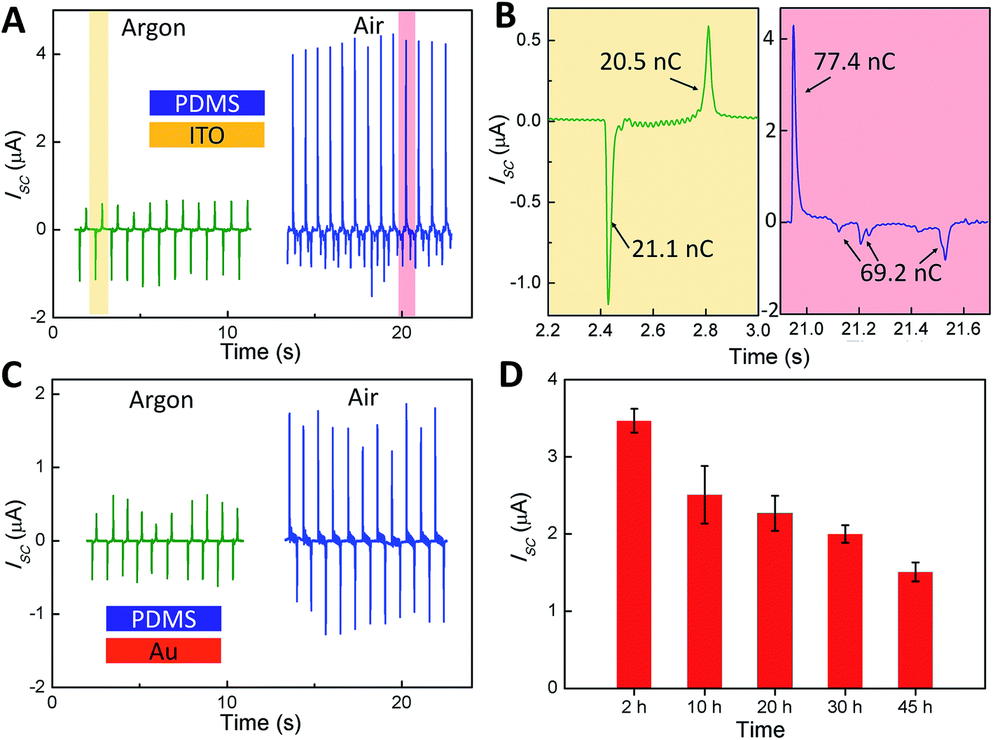 | ||
| Fig. 4 Influence of the operation environment and the material properties on the output preference of the TENG. (A) Performance comparison of the TENG devices using PDMS and ITO as the triboelectric surfaces in an ambient environment and in an argon environment, respectively. (B) The enlarged views of a single current peak marked in (A). The amounts of transferred charges from a single displacement have been calculated. (C) Short-circuit currents of the TENG devices using PDMS and Au as the triboelectric surfaces in an ambient environment and in an argon environment, respectively. (D) Performance of the TENG devices using a PDMS thin film with different curing times. | ||
To gain more insights into the nature of the charged surface, we performed a series of comparative experiments using Raman spectroscopy and X-ray photoelectron spectroscopy (XPS). From the Raman spectrum in Fig. 5A, it is obvious that some materials are transferred from the PDMS to ITO surface during the triboelectric process, resulting in a significant change in the Raman spectra of ITO surfaces before and after triboelectrification. Moreover, the peak at ∼495 cm−1 assigned to the symmetric stretches of the Si–O–Si groups disappeared completely on the tribocharged ITO surface.34 It indicates that the bond breaking of Si–O–Si groups occurred and the charged polymer fragments being transferred. In other words, the tribocharge generation of the PDMS surface is probably due to the bond breaking of the Si–O–Si groups. For XPS characterization, after the UV–ozone treatment, the Si/C and O/C ratios of the PDMS surface were significantly increased due to the breaking of methyl groups (Si–CH3) and the formation of silanol groups (Si–OH). However, there is no difference in the types and ratios of elements between the triboelectric charged and intact samples. One possible reason is that the charges or charged mass produced by triboelectrification decayed with time before XPS measurements.21 To get a deep insight into the triboelectric mechanism, we need to use sensitive spectroscopic methods for in situ characterization of the charged product, and further research into this issue is ongoing. The study of the mechanism of triboelectric electrification and charge transfer from the microscopic perspective will help us to reasonably design the structure and improve the output performance of the TENG.
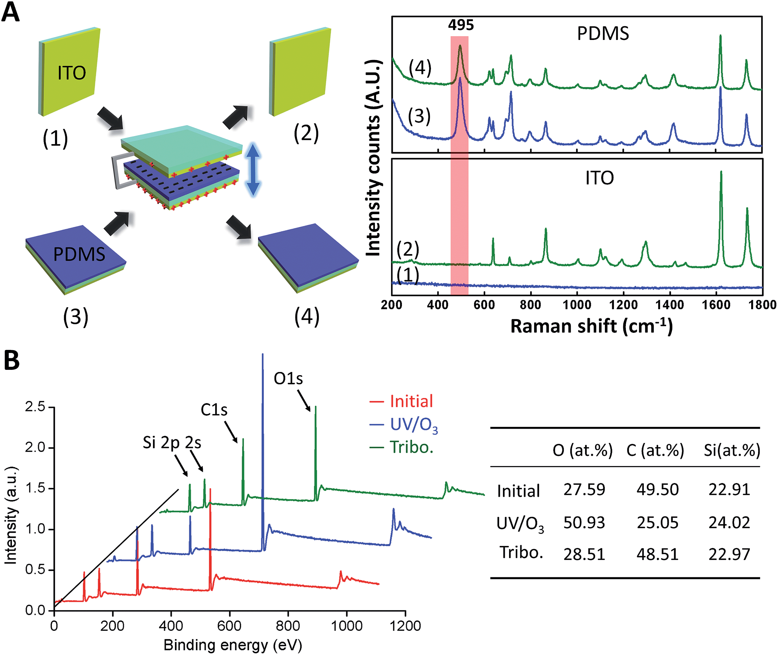 | ||
| Fig. 5 (A) Raman spectra of the ITO surface before (1) and after triboelectrification (2), and the PDMS surface before (3) and after triboelectrification (4), respectively. (B) XPS spectra and atomic composition of PDMS films before the surface modification, after the UV–ozone treatment, or rubbed by an ITO film in an ambient environment, respectively. | ||
4. Conclusion
In summary, we have successfully demonstrated a simple and effective design of a transparent, flexible TENG. It can significantly improve the output efficiency by using an ITO electrode directly as one of the friction surfaces and an arched structure or spacers in the structure. A maximum output up to 200 V and 7 μA at a current density of ∼0.78 μA cm−2, and an effective electrical power up to 0.45 mW at a load resistance of ∼30 MΩ, which is almost ten times as high as that of the previously reported transparent TENG, is obtained. To circumvent the intrinsic problem of light scattering of the patterned surface, a full TENG device prepared with a flat PDMS film shows a high transmittance of ∼78%. We also investigated the influence of the surface modification and surrounding environment on the output performance. It is found that the UV–ozone treatment will make the PDMS surface charged. During the triboelectric process, the PDMS surface is sensitive to atmospheric oxygen and water and the output performance in the atmosphere is much higher than that in the argon atmosphere. We believe that the tribocharge generation of the PDMS surface is probably due to the bond breaking of Si–O–Si polymer chains, and is closely related to the surface properties and surrounding environment. The transparent TENG technology exhibits distinct advantages as a simple, high-powered, cost-effective, and scalable approach. Potential applications range from flexible electronics and low-power portable devices to self-powered systems for touchscreens, electronic displays, and even optoelectronics systems.Acknowledgements
This research was supported by the “thousands talents” program for pioneer researcher and his innovation team, China, and the Beijing City Committee of science and technology project (Z131100006013004, Z131100006013005). The authors would like to thank Prof. Jianfeng Li, Prof. Deying Wu and Weiwei Wu for helpful discussions and assistance in experiments.References
- D. S. Ginley and C. Bright, MRS Bull., 2000, 25, 15–18 CrossRef CAS
.
- K. Nomura, H. Ohta, A. Takagi, T. Kamiya, M. Hirano and H. Hosono, Nature, 2004, 432, 488–492 CrossRef CAS PubMed
- J. F. Wager, Science, 2003, 300, 1245–1246 CrossRef CAS PubMed
- Z. C. Wu, Z. H. Chen, X. Du, J. M. Logan, J. Sippel, M. Nikolou, K. Kamaras, J. R. Reynolds, D. B. Tanner, A. F. Hebard and A. G. Rinzler, Science, 2004, 305, 1273–1276 CrossRef CAS PubMed
- Z. L. Wang and J. H. Song, Science, 2006, 312, 242–246 CrossRef CAS PubMed
- Z. L. Wang and W. Z. Wu, Angew. Chem., Int. Ed., 2012, 51, 11700–11721 CrossRef CAS PubMed
- K. I. Park, M. Lee, Y. Liu, S. Moon, G. T. Hwang, G. Zhu, J. E. Kim, S. O. Kim, D. K. Kim, Z. L. Wang and K. J. Lee, Adv. Mater., 2012, 24, 2999–3004 CrossRef CAS PubMed
- B. Meng, W. Tang, X. S. Zhang, M. D. Han, W. Liu and H. X. Zhang, Nano Energy, 2013, 2, 1101–1106 CrossRef CAS PubMed
- K. Y. Lee, D. Kim, J. H. Lee, T. Y. Kim, M. K. Gupta and S. W. Kim, Adv. Funct. Mater., 2014, 24, 37–43 CrossRef CAS
- F. R. Fan, Z. Q. Tian and Z. L. Wang, Nano Energy, 2012, 1, 328–334 CrossRef CAS PubMed
- Z. L. Wang, ACS Nano, 2013, 7, 9533–9557 CrossRef CAS PubMed
- G. Zhu, Y. S. Zhou, P. Bai, X. S. Meng, Q. Jing, J. Chen and Z. L. Wang, Adv. Mater., 2014, 26, 3788–3796 CrossRef CAS PubMed
- F. R. Fan, L. Lin, G. Zhu, W. Z. Wu, R. Zhang and Z. L. Wang, Nano Lett., 2012, 12, 3109–3114 CrossRef CAS PubMed
- Y. H. Ko, S. H. Lee, J. W. Leem and J. S. Yu, RSC Adv., 2014, 4, 10216–10220 RSC
- Y. H. Ko, N. Goli, S. H. Lee and J. S. Yu, ACS Appl. Mater. Interfaces, 2014, 6, 6631–6637 CAS
- S. Kim, M. K. Gupta, K. Y. Lee, A. Sohn, T. Y. Kim, K. S. Shin, D. Kim, S. K. Kim, K. H. Lee and H. J. Shin, Adv. Mater., 2014, 26, 3918–3925 CrossRef CAS PubMed
- L. M. Zhang, F. Xue, W. Du, C. B. Han, C. Zhang and Z. L. Wang, Nano Res., 2014 DOI:10.1007/s12274-014-0484-1
- L. S. McCarty and G. M. Whitesides, Angew. Chem., Int. Ed., 2008, 47, 2188–2207 CrossRef CAS PubMed
- C. Y. Liu and A. J. Bard, Chem. Phys. Lett., 2009, 480, 145–156 CrossRef CAS PubMed
- H. T. Baytekin, B. Baytekin, T. M. Hermans, B. Kowalczyk and B. A. Grzybowski, Science, 2013, 341, 1368–1371 CrossRef CAS PubMed
- H. T. Baytekin, A. Z. Patashinski, M. Branicki, B. Baytekin, S. Soh and B. A. Grzybowski, Science, 2011, 333, 308–312 CrossRef CAS PubMed
- Y. S. Zhou, Y. Liu, G. Zhu, Z. H. Lin, C. F. Pan, Q. S. Jing and Z. L. Wang, Nano Lett., 2013, 13, 2771–2776 CrossRef CAS PubMed
- G. Zhu, C. F. Pan, W. X. Guo, C. Y. Chen, Y. S. Zhou, R. M. Yu and Z. L. Wang, Nano Lett., 2012, 12, 4960–4965 CrossRef CAS PubMed
- S. H. Wang, L. Lin and Z. L. Wang, Nano Lett., 2012, 12, 6339–6346 CrossRef CAS PubMed
- S. M. Niu, S. H. Wang, L. Lin, Y. Liu, Y. S. Zhou, Y. F. Hu and Z. L. Wang, Energy Environ. Sci., 2013, 6, 3576–3583 Search PubMed
- L. S. McCarty, A. Winkleman and G. M. Whitesides, J. Am. Chem. Soc., 2007, 129, 4075–4088 CrossRef CAS PubMed
- H. T. Baytekin, B. Baytekin, J. T. Incorvati and B. A. Grzybowski, Angew. Chem., Int. Ed., 2012, 51, 4843–4847 CrossRef CAS PubMed
- B. Baytekin, H. T. Baytekin and B. A. Grzybowski, J. Am. Chem. Soc., 2012, 134, 7223–7226 CrossRef CAS PubMed
- Z. H. Lin, Y. N. Xie, Y. Yang, S. H. Wang, G. Zhu and Z. L. Wang, ACS Nano, 2013, 7, 4554–4560 CrossRef CAS PubMed
- Z. H. Lin, G. Zhu, Y. S. Zhou, Y. Yang, P. Bai, J. Chen and Z. L. Wang, Angew. Chem., Int. Ed., 2013, 52, 5065–5069 CrossRef CAS PubMed
- X. S. Zhang, M. D. Han, R. X. Wang, B. Meng, F. Y. Zhu, X. M. Sun, W. Hu, W. Wang, Z. H. Li and H. X. Zhang, Nano Energy, 2014, 4, 123–131 CrossRef CAS PubMed
- H. Hillborg, N. Tomczak, A. Olah, H. Schonherr and G. J. Vancso, Langmuir, 2004, 20, 785–794 CrossRef CAS
- H. Makamba, J. H. Kim, K. Lim, N. Park and J. H. Hahn, Electrophoresis, 2003, 24, 3607–3619 CrossRef CAS PubMed
- L. Jayes, A. P. Hard, C. Sene, S. F. Parker and U. A. Jayasooriya, Anal. Chem., 2003, 75, 742–746 CrossRef CAS
Footnotes |
| † Electronic supplementary information (ESI) available. See DOI: 10.1039/c4ta02747g |
| ‡ F. R. F. and J. L. contributed equally to this work. |
| This journal is © The Royal Society of Chemistry 2014 |