Assembling CdSe/ZnS core–shell quantum dots on localized DNA nanostructures†
Junwye Leea,
Jongtaek Leeb,
Sung Mo Yeonb,
Sunmin Minb,
Jinwoo Kimb,
Hyeokwoo Choib,
Sunho Kimb,
Jonghyun Koob,
Kyungseob Kimb,
Sung Ha Park*a and
Yonghan Roh*b
aSungkyunkwan Advanced Institute of Nanotechnology (SAINT) and Department of Physics, Sungkyunkwan University, Suwon 440-746, Korea. E-mail: sunghapark@skku.edu
bSungkyunkwan Advanced Institute of Nanotechnology (SAINT) and School of Information & Communication Engineering, Sungkyunkwan University, Suwon 440-746, Korea. E-mail: yhroh@skku.edu
First published on 8th October 2014
Abstract
We have demonstrated the assembly of CdSe/ZnS core–shell quantum dots (Qdots) on DNA templates that could potentially be used in practical devices and sensors. Qdots were aligned on one and two dimensional DNA nanostructures through electrostatic interaction between Qdots and DNA nanostructures. About 2 to 3 times larger adsorption ratios of Qdots on DNA templates were observed on both positively and negatively charged substrates. Moreover, assembled Qdots on DNA templates exhibit significant improvement in electric characteristics with a distinct semiconductor-like plateau. The results obtained in this research show the specific complementary relationship between Qdots and DNA nanostructures: the DNA nanostructures guide precise control of Qdot assembly on desired places and assembled Qdots help to increase the functionality of complexes. These approaches open up opportunities to control accurate positioning of specific nano and biomaterials with full functionality and efficiency in a given system.
Fluorescent materials have been of great interest because of their remarkable possible applications in interdisciplinary fields such as biosensors for diagnosis,1,2 photonics3,4 and electronics.5 In addition, nanoscience and nanotechnology, which have rapidly developed within recent years, have provided a low-dimensional nanometer-sized system defining a new research field in condensed-matter physics. These systems have much in common with atoms, allowing the artificial quantum confinement with only a few electrons, but they are man-made structures fabricated in the laboratory. These materials are called quantum dots (Qdots), which provide distinct variation of optical and electronic properties with particle size due to quantum confinement in three spatial dimensions.6,7 The properties of Qdots are closely related with the energy gap between the valence and conduction bands, which are in inverse proportion to the size of the Qdots. Generally, the Qdots generate stable homogeneous light with higher frequencies as the size becomes smaller, resulting in a color shift from red to blue. In addition, the ability to control a few electrons provides the ability to tailor electronic properties.
Recent research on Qdots has focused on the practical usage of Qdots in current applications.1–5 These applications are usually realized by fine control mechanisms of aligning Qdots on desired regions or specific sites on target materials. Consequently, various control techniques have been established in recent years such as submicron-scale imprinting3 and bio-assays with biotin–avidin bonds.8,9 Even though conventional techniques have provided great promise for submicron-scale controllability of Qdots, new control techniques are still required to open up novel approaches to Qdots in different disciplines. As one prime candidate, a DNA molecule has great potential to effectively provide accurate control of Qdot attachment in desired shapes dictated by templates. Due to the notable base-sequence programmability and structural plasticity, DNA molecules can be fabricated into various shapes of artificially designed DNA nanostructures with nano-scale feature resolution, which may serve as a template for Qdot arrangement.10–14 As an intermediate step toward this, we report the complementary relationship between DNA nanostructures and Qdots. Here, Qdots and DNA show a complementary relationship, which aids in overcoming their limited characteristics, i.e., difficulty of accurate arrangement and poor conductivity, respectively.
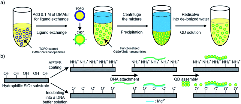
A water-soluble CdSe/ZnS core–shell Qdot with a positively charged capping ligand was prepared as follows. Tri-n-octylphosphine oxide (TOPO)-capped Qdots with chemical composition gradients were synthesized through a single-step method using reactivity differences among precursors.15–17 The Qdots were then precipitated with ethanol, and separated by centrifugation and decantation. While the precipitate steps were repeated, the capping ligand of Qdots, oleic acid, was completely washed away. Subsequently, the precipitate was dissolved in chloroform. In order to functionalize Qdots with positively charged ligands, 300 μL of a methanolic solution (0.1 mM) of 2-dimethylaminoethanethiol (DMAET) was added into 1 mL of a Qdot solution (2 mg mL−1). The mixture was incubated until the ligand-exchanged Qdots fully precipitated. Again, the precipitate was washed with methanol twice to remove excess DMAET and was dissolved in 1 mL of de-ionized water (DI-water). Finally, about 3.71 ± 0.44 nm Qdots with a 32.11 mV surface charge were synthesized (Fig. 1a). Overall optical analyses of the ligand exchange and zeta-potential are discussed in Fig. S1 and S2 in the ESI.†
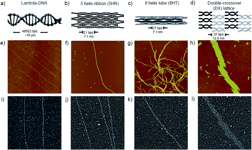
Our strategies to assembly Qdots on DNA templates were carried out in two different ways. For λ-DNA (48![[thin space (1/6-em)]](https://www.rsc.org/images/entities/char_2009.gif) 502 base pairs), a 3-aminopropyltrithoxysilane (APTES) monolayer was synthesized on SiO2 substrate by a self-assembling procedure in a toluene solution,18 whereas the piranha-treated SiO2 (p-SiO2) substrate was prepared for other DNA nanostructures. In contrast to the positive nature of the APTES-coated surface, the p-SiO2 substrate has a negative charge due to deprotonated silanol groups (Si–O–) on the SiO2 surface (Fig. 1b).19,20 For various shapes of DNA templates, three different types of DNA nanostructures were prepared. Double-crossover (DX) crystals were constructed from two different DX tiles consisting of two adjacent duplex DNAs.10 In this system, two adjacent duplex DNAs are strongly tethered by two crossover junctions in which there are 16 nucleotides to make an angle of 540°, i.e., one and a half full turns. Both 5 helix ribbon (5 HR) and 8 helix tube (8 HT) nanostructures were fabricated from 42 base-pair long single-strands.11 Detailed base sequences are given in the ESI Fig. S3 and S4.† Immobilization of each DNA nanostructure was achieved by a molecular combing process for λ-DNA,18 and the simple sample solution deposition method for other DNA nanostructures, respectively. Schematic diagrams of each DNA template are illustrated in Fig. 2a–d, and corresponding atomic force microscopy (AFM) images are displayed in the same column (Fig. 2e–h). Finally, the Qdot attachment was then achieved by depositing a 10 μL droplet of Qdot solution onto the DNA templates for 5 min. Scanning electron microscopy (SEM) images in Fig. 2i–l and transmission electron microscopy (TEM) images in Fig. S5 in the ESI† show well-aligned granular Qdots on corresponding DNA templates.
502 base pairs), a 3-aminopropyltrithoxysilane (APTES) monolayer was synthesized on SiO2 substrate by a self-assembling procedure in a toluene solution,18 whereas the piranha-treated SiO2 (p-SiO2) substrate was prepared for other DNA nanostructures. In contrast to the positive nature of the APTES-coated surface, the p-SiO2 substrate has a negative charge due to deprotonated silanol groups (Si–O–) on the SiO2 surface (Fig. 1b).19,20 For various shapes of DNA templates, three different types of DNA nanostructures were prepared. Double-crossover (DX) crystals were constructed from two different DX tiles consisting of two adjacent duplex DNAs.10 In this system, two adjacent duplex DNAs are strongly tethered by two crossover junctions in which there are 16 nucleotides to make an angle of 540°, i.e., one and a half full turns. Both 5 helix ribbon (5 HR) and 8 helix tube (8 HT) nanostructures were fabricated from 42 base-pair long single-strands.11 Detailed base sequences are given in the ESI Fig. S3 and S4.† Immobilization of each DNA nanostructure was achieved by a molecular combing process for λ-DNA,18 and the simple sample solution deposition method for other DNA nanostructures, respectively. Schematic diagrams of each DNA template are illustrated in Fig. 2a–d, and corresponding atomic force microscopy (AFM) images are displayed in the same column (Fig. 2e–h). Finally, the Qdot attachment was then achieved by depositing a 10 μL droplet of Qdot solution onto the DNA templates for 5 min. Scanning electron microscopy (SEM) images in Fig. 2i–l and transmission electron microscopy (TEM) images in Fig. S5 in the ESI† show well-aligned granular Qdots on corresponding DNA templates.
The Qdot attachment was based on electrostatic interaction between Qdot nanoparticles and DNA molecules. Due to the positively charged amino groups on the Qdot surface, they electrostatically interact with negatively charged phosphate backbones of a DNA molecule. As clearly shown in Fig. 2i, Qdots are assembled on λ-DNA templates, leaving a large empty section of the APTES surface. It is important to note that the repulsive force from the positively charged APTES surface results in a ∼460% increase in adsorption ratio on λ-DNA templates compared to the background (calculation shown in Fig. S6 in the ESI†). A somewhat different Qdot arrangement was obtained when the Qdot solution was deposited onto the DNA nanostructures immobilized onto a p-SiO2 substrate. In contrast to the APTES-coated surface, the p-SiO2 surface has a ∼35 mV negative charge due to the deprotonated Si–O− groups under a normal physiological DNA buffer, 1× TAE/Mg2+ tris-acetate-EDTA (40 mM tris, 1 mM EDTA (pH 8.0), 12.5 mM Mg(Ac)2). Consequently, the electrostatic nature allows Qdot assembly on the DNA nanostructures as well as the p-SiO2 surface. The analyses of Qdot distribution exhibits ∼360, ∼300, ∼270% increases in Qdot adsorption ratio on 5 HR, 8 HT, DX DNA nanostructures, respectively (Fig. S6 in the ESI†). Due to the negatively charged p-SiO2 substrate, the adsorption ratio on the substrate is relatively increased compared to the APTES case, as shown in Fig. 2i–l.
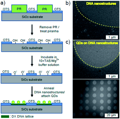
The accurate assembly of Qdots onto the desired places was realized by a substrate-assisted growth (SAG) method such that DNA nanostructures were directly self-assembled onto the lithographically patterned SiO2 substrate during the annealing process.21 Fig. 3a displays the patterning process of SiO2.22 Photoresist (PR) patterns were formed by covering a PR layer deposited on a SiO2 substrate with a mask and exposing it to UV light. After development, the substrate was dipped in an octadecyltrichlorosilane (OTS) and hexane mixture. The PR patterns were removed completely and the substrate was again dipped in a piranha solution (H2O2 (30%):H2SO4 (96%) = 1![[thin space (1/6-em)]](https://www.rsc.org/images/entities/char_2009.gif) :
:![[thin space (1/6-em)]](https://www.rsc.org/images/entities/char_2009.gif) 2), after which both the patterned substrate and individual DX DNA strand were combined in a test tube. These samples were cooled slowly from 95 °C to 25 °C by placing the test-tube in 2 L boiling water in a styrofoam box for 24 hours to facilitate hybridization. Successful fabrication of DX DNA lattices using this method was confirmed through SEM images shown in Fig. 3b. The yellow dashed lines indicate the boundaries between the DX DNA lattices and the OTS monolayers. Finally, Qdot alignment was achieved by depositing a 10 μL droplet of Qdot solution onto the DX DNA lattices for 5 min. Fig. 3c exhibits Qdots assembled onto the desired area, where the accuracy of the Qdot assembly on the lithographic patterns can be seen. Most of images show a slightly lower Qdot adsorption ratio (∼190%) compared to OTS-covered regions (Fig. S7 in the ESI†). The decrease of adsorption ratio of Qdots may stem from the change of surface roughness during the OTS-patterning process shown in Fig. 3a. Compared to the p-SiO2 surface, the OTS regions after piranha treatment has a relatively high surface roughness of ∼0.8 nm, and the topology seems granular (Fig. S8 in the ESI†). Due to this uneven surface of OTS, Qdots deposited non-specifically on it could not be completely removed during the washing process.
2), after which both the patterned substrate and individual DX DNA strand were combined in a test tube. These samples were cooled slowly from 95 °C to 25 °C by placing the test-tube in 2 L boiling water in a styrofoam box for 24 hours to facilitate hybridization. Successful fabrication of DX DNA lattices using this method was confirmed through SEM images shown in Fig. 3b. The yellow dashed lines indicate the boundaries between the DX DNA lattices and the OTS monolayers. Finally, Qdot alignment was achieved by depositing a 10 μL droplet of Qdot solution onto the DX DNA lattices for 5 min. Fig. 3c exhibits Qdots assembled onto the desired area, where the accuracy of the Qdot assembly on the lithographic patterns can be seen. Most of images show a slightly lower Qdot adsorption ratio (∼190%) compared to OTS-covered regions (Fig. S7 in the ESI†). The decrease of adsorption ratio of Qdots may stem from the change of surface roughness during the OTS-patterning process shown in Fig. 3a. Compared to the p-SiO2 surface, the OTS regions after piranha treatment has a relatively high surface roughness of ∼0.8 nm, and the topology seems granular (Fig. S8 in the ESI†). Due to this uneven surface of OTS, Qdots deposited non-specifically on it could not be completely removed during the washing process.
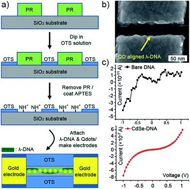
Another interesting feature obtained from the Qdot-DNA complex is the increase in conductivity. In recent years, the promising aspect of using DNA molecules in nanoelectronic circuits has been highlighted because characteristics of self-assembly and self-alignment may help to provide the particular resolution of nano-scale wiring and positioning.23,24 Although previous works have reported the practical usage of DNA molecules in electronic devices with fundamental research on its electric behaviour in different ways, realizing a DNA electronic circuit has still faced some problems due to low electric conductivity.25,26 In order to measure the change of conductivity through DNA molecules, we prepared immobilized λ-DNA on an 1-D shape patterned substrate. The 1-D patterned substrate was prepared by a typical OTS-coating process as mentioned above. The immobilization of λ-DNA on a target site was achieved by the molecular combing method with the same direction of 1-D patterns, and the Qdots were then assembled by depositing a 10 μL droplet of Qdot sample for 5 min. After that, two terminal gold electrodes with a 40 nm gap were made by electron beam lithography exactly on the immobilized Qdot-λ-DNA nanowire. Fig. 4b exhibits a SEM image of the Qdot-λ-DNA nanowire with ∼5 nm feature size between gold electrodes. The current (I)–voltage (V) curve measured at room temperature shows a significant current increase with a semiconductor-like plateau (conductance gap) of about 1.1 eV, whereas the noise level current of ∼pA was detected from a bare λ-DNA duplex shown in Fig. 4c. We prepared about 20 samples. Among them, only 3 samples (∼15% of total measured samples) gave us reliable data which showed a current increase with a semiconductor-like plateau. This suggests that this system would provide a few orders of current increase with semiconducting behaviour through the particular shape of DNA nanostructures. From the literature, these semiconductor-like characteristics of the current flow through these hybrid nanowires were explained nicely by tunnelling – an electron transfer through a series of sites separated by potential wells – and hopping mechanisms, that is, a thermally activated process where the electron transfer follows a classical Arrhenius relationship, k = A![[thin space (1/6-em)]](https://www.rsc.org/images/entities/char_2009.gif) exp(−Ea/kBT), where k, A, Ea, kB, and T were the hopping rate constant, the prefactor, the activation energy, the Boltzmann constant, and the temperature, respectively.27–29
exp(−Ea/kBT), where k, A, Ea, kB, and T were the hopping rate constant, the prefactor, the activation energy, the Boltzmann constant, and the temperature, respectively.27–29
In conclusion, we have demonstrated the assembly of CdSe/ZnS core–shell Qdots on DNA templates that could potentially be used in practical devices and sensors. Qdots on the specific DNA templates were aligned and formed as a specific shape of templates through electrostatic interaction between Qdots and DNA molecules. About 2 to 3 times larger adsorption ratios of Qdots on DNA templates were observed on both positively and negatively charged substrates. Moreover, assembled Qdots on DNA templates exhibit significant improvement in electric characteristics with a distinct semiconductor-like plateau. In short, the results obtained in this research show the specific complementary relationship between Qdots and DNA nanostructures: the DNA nanostructures guide precise control of Qdot assembly on desired places and assembled Qdots help to increase the functionality of complexes. These approaches open up opportunities to control accurate positioning of specific nano and biomaterials with full functionality and efficiency in given a system. Due to the rapid development of structural DNA nanotechnology,30 we could develop more sophisticated nanodevices and sensors templated by DNA nanostructures with better performance.
Acknowledgements
We thank J. Shin for helpful discussions. This research was supported by the Basic Science Research Program through the National Research Foundation of Korea (NRF) funded by the Ministry of Science, ICT & Future Planning (NRF-2012R1A2A2A02046890).Notes and references
- P. Zrazhevskiy, M. Sena and G. Xiaohu, Chem. Soc. Rev., 2010, 39, 4326 RSC.
- D. Geibler, L. J. Charbonnière, R. F. Ziessel, N. G. Butlin, H. Löhmannsröben and N. Hildebrandt, Angew. Chem., Int. Ed., 2010, 49, 1396 CrossRef PubMed.
- T. H. Kim, K. S. Cho, E. K. Lee, S. J. Lee, J. Chae, J. W. Kim, D. H. Kim, J. Y. Kwon, G. Amaratunga, S. Y. Lee, B. L. Choi, Y. Kuk, J. M. Kim and K. Kim, Nat. Photonics, 2011, 5, 176 CrossRef CAS.
- E. Jang, S. Jun, H. Jang, J. Lim, B. Kim and Y. Kim, Adv. Mater., 2010, 22, 3076 CrossRef CAS PubMed.
- S. D. Franceschi, L. Kouwenhoven, C. Schönenberger and W. Wernsdorfer, Nat. Nanotechnol., 2010, 5, 703 CrossRef PubMed.
- D. Bera, L. Qian, T. K. Tseng and P. H. Holloway, Materials, 2010, 3, 2260 CrossRef CAS PubMed.
- S. Kiravittaya, A. Rastelli and O. G. Schmidt, Rep. Prog. Phys., 2009, 72, 046502 CrossRef.
- F. Chen and D. Gerion, Nano Lett., 2004, 4, 1827 CrossRef CAS.
- M. Bäumle, D. Stamou, J. M. Segura, R. Hovius and H. Vogel, Langmuir, 2004, 20, 3828 CrossRef.
- E. Winfree, F. Liu, L. A. Wenzler and N. C. Seeman, Nature, 1998, 394, 539 CrossRef CAS PubMed.
- P. Yin, R. F. Hariadi, S. Sahu, H. M. T. Choi, S. H. Park, T. H. LaBean and J. H. Reif, Science, 2008, 321, 824 CrossRef CAS PubMed.
- J. Sharma, R. Chhabra, Y. Liu, Y. Ke and H. Yan, Angew. Chem., Int. Ed., 2006, 45, 730 CrossRef CAS PubMed.
- S. M. Douglas, H. Dietz, T. Leidl, B. Hogberg, F. Graf and W. M. Shih, Nature, 2009, 459, 414 CrossRef CAS PubMed.
- J. Lee, S. Hamada, R. Amin, S. Kim, A. Kulkarni, T. Kim, Y. Roh, S. Murata and S. H. Park, Small, 2012, 8, 374 CrossRef CAS PubMed.
- W. K. Bae, K. Char, H. Hur and S. Lee, Chem. Mater., 2008, 20, 531 CrossRef CAS.
- M. Artemyev, D. Kisiel, S. Abmiotko, M. N. Antipina, G. B. Khomutov, V. V. Kislov and A. A. Rakhnyanskaya, J. Am. Chem. Soc., 2004, 126, 10594 CrossRef CAS PubMed.
- A. Hoshino, K. Fujioka, T. Oku, M. Suga, Y. F. Sasaki, T. Ohta, M. Yasuhara, K. Suzuki and K. Yamamoto, Nano Lett., 2004, 4, 2163 CrossRef CAS.
- H. J. Kim, Y. Roh and B. Hong, Langmuir, 2010, 26, 18315 CrossRef CAS PubMed.
- J. P. Brunelle, Pure. Appl. Chem., 1978, 50, 1211 CrossRef CAS.
- K. Kamada, M. Tokutomi, N. Enomoto and J. Hojo, J. Mater. Chem., 2005, 15, 3388 RSC.
- J. Lee, S. Kim, J. Kim, C. W. Lee, Y. Roh and S. H. Park, Angew. Chem., Int. Ed., 2011, 50, 9145 CrossRef CAS PubMed.
- Y. Wang and M. Lieberman, Langmuir, 2003, 19, 1159 CrossRef CAS.
- G. Maubach, D. Born, A. Csàki and W. Fritzsche, Small, 2005, 1, 619 CrossRef CAS PubMed.
- J. Lund, J. Dong, Z. Deng, C. Mao and B. A. Parviz, Nanotechnology, 2006, 17, 2752 CrossRef CAS.
- F. D. Lewis, T. Wu, Y. Zhang, R. L. Letsinger, S. R. Greenfield and M. R. Wasielewski, Science, 1997, 277, 673 CrossRef CAS.
- A. Rakitin, P. Aich, C. Papadopoulos, Y. Kobzar, A. S. Bedeneev, J. S. Lee and J. M. Xu, Phys. Rev. Lett., 2001, 86, 3670 CrossRef CAS.
- R. L. McCreery, Chem. Mater., 2004, 16, 4477 CrossRef CAS.
- L. Luo, S. H. Choi and C. D. Frisbie, Chem. Mater., 2011, 23, 631 CrossRef CAS.
- L. V. Govor, G. H. Bauer, G. Reiter and J. Parisi, Phys. Status Solidi A, 2013, 210, 1107 CrossRef CAS.
- R. Amin, S. Kim, S. H. Park and T. H. LaBean, NANO, 2009, 4, 119 CrossRef CAS.
Footnote |
| † Electronic supplementary information (ESI) available: TEM images, EDS spectra, optical and zeta-potential analyses of CdSe/ZnS core–shell Qdots, DNA base sequences of DX, 5 HR and 8 HT structures, adsorption ratio calculation, and roughness analysis of bare/OTS-coated p-SiO2 substrates. See DOI: 10.1039/c4ra04382k |
| This journal is © The Royal Society of Chemistry 2014 |


