 Open Access Article
 This Open Access Article is licensed under a
 Creative Commons Attribution 3.0 Unported Licence
Computational modelling of a graphene Fresnel lens on different substrates
Sunan Denga,
Ali K. Yetisenb,
Kyle Jianga and
Haider Butt*a
aSchool of Mechanical Engineering, The University of Birmingham, Birmingham B15 2TT, UK. E-mail: h.butt@bham.ac.uk; Tel: +44 (0)121 4158623
bDepartment of Chemical Engineering and Biotechnology, University of Cambridge, Cambridge CB2 1QT, UK
First published on 10th July 2014
Abstract
Graphene being the thinnest material known has a lot of potential applications in compact systems, where the size and weight are limited. Here we study through computational modelling a graphene based Fresnel zone plate lens. The optical properties of graphene and the focusing response of the lens are studied for the 850 and 1550 nm wavelengths. The lens performance can be tuned by adjusting the Fermi level of graphene and the number of layers. The effects of substrates (such as glass and SiO2/Si) on the performance of graphene lens are also analysed. The result presented can also be used in optimising the performance of other graphene based optical devices, such as scattering from graphene based transparent electrodes.
I. Introduction
A Fresnel zone plate focuses light by diffracting from a binary mask that blocks part of the radiation.1 Unlike traditional lenses, a Fresnel zone plate has a flat surface with a set of radially symmetric rings, which alternate between opaque and transparent.2 As a Fresnel zone plate offers the possibility of designing high numerical aperture (NA) lens with low weight and small volume, it has been widely used in silicon based electronics with various applications, such as optical interconnects,3 integrated optics,4 beam focusing5,6 and maskless lithography systems.7A thin lens has a thickness that is negligible compared to the focal length. Currently, imaging in traditional curved lenses is limited by distortions. Although the aberrations could be corrected by complex optimization techniques, such as aspheric shapes or multilens design, much cost and space will be needed, especially in mid-and near-infrared wavelength range. An alternative is to develop ultrathin lenses with low weight and small volume. Fresnel zone plate offers a solution by introducing abrupt changes of optical properties, which eliminates the propagation effect.
The ultrathin lens, with a thickness of 60 nm, fabricated by Federico Capasso et al.,8 has attracted enormous attention as it is considered to be a milestone to improve consumer technology. As graphene is the thinnest and most promising material, we studied the properties of graphene Fresnel lens by FDTD method. Graphene, the first 2D material practically realized,9 is an optoelectronic material with a set of superior properties, such as high optical transparency, low reflectance and high carrier mobility at room temperature.10 Accompanying the appealing properties of graphene is its ability to be tunable. The properties of graphene could be altered via changing the charge carriers (electrons or holes), through for example electrical gating11 or chemical doping.12 When a bias voltage is applied, the optical gap, with the energy proportional to the voltage, will open up. Under normal conditions, electrical gating can produce chemical potential of EF ≈ 1 eV,11 which corresponds to additional carriers with concentration13 of n ∼ 7 × 1013 cm−2. As photons are uncharged, it is challenging to control them via electrical means. However, graphene Fresnel lens offers an effective way to manipulate the flow of light energy by changing graphene's Fermi level.
A few papers have been focus on confining light by carbon nanotubes.14–17 In our previous works,15,16 we made carbon nanotubes (CNTs) based Fresnel lenses, in which CNT arrays act as dark structures because of low reflection, high absorption and random surface scattering. The properties of CNTs (semiconducting or metallic) depend largely on the chiral angle of graphene sheet.18 However, it's difficult to synthesize large quantities of CNTs with the same chirality. Also CNTs don't have the perfect tunable absorption as graphene, so we propose tunable graphene Fresnel lens here. Beside the tunability, graphene has larger surface area and much thinner than CNTs. So graphene could be used in a complementary way for photonic-nanotube hybrid devices.
Some literature exists on graphene based flat lenses,19–22 and the focus has been on making plasmonic lenses working in terahertz range. In some works, people use photonic crystal to focus light and graphene works as a gate to achieve tunability.23,24 Compared with their works, we enable both focusing and tunablity function in graphene with two advantages: lower optical losses and greater compactness. Compared with photonic crystal, graphene could have very low optical losses via adjusting its Fermi level to get high carrier density.25
In Karabiyik's work,26,27 a tunable THz Fresnel lenses based on 2D electron gas at AlGaN/GaN interface and on few-layer graphene sheets has been proposed. In this study, graphene works as a gate and metal is used as the opaque zones, so the lens is not thin enough due to its multi-layers structure.
In our work, we design graphene to be the opaque zones to explore the thinnest possible lens for compact optical systems. Single layer graphene has a universal optical conductivity28 of G0 = e2/(4ℏ) ≈ 6.08 × 10⁻⁵ Ω−1, where e is the electronic charge and ℏ is the reduced constant. The transmittance of graphene could be derived from: 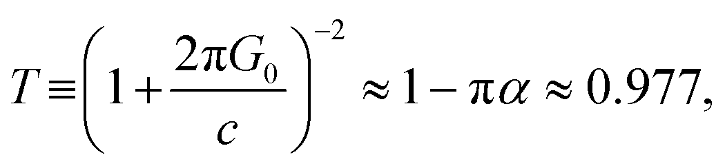 where
where 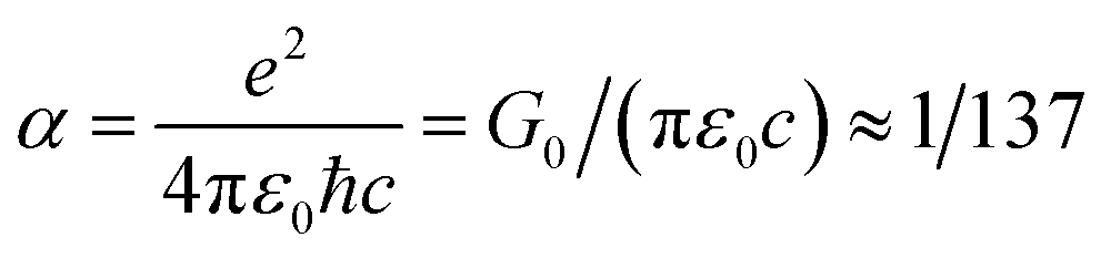 is the fine structure constant.29 In the visible regime, the opacity of graphene will increase linearly with the layers of graphene. For N layers graphene, the transmittance could be written as:30 T ≅ 1 − Nπα. Thus it is possible to use multi-layer graphene as the opaque zone of the Fresnel lenses.
The tunable properties of the graphene Fresnel lens under light of wavelengths of 850 nm and 1550 nm, which are two important windows in optical communication, are studied by changing the Fermi level of graphene. Our research shows clear tunable lensing effect of graphene Fresnel lens under the two wavelengths. In comparison to THz, we studied the tunability of graphene Fresnel lens in optical regime, which has potential applications in solar cells, photodiodes, as well as compact optical devices, such as cameras and medical imaging systems. Due to their manufacturing limits, graphene devices are usually made on different substrates, for example glass and SiO2/Si. Hence, the interference effect on graphene Fresnel lens caused by different substrates is also discussed.
II. Tunable optical properties of graphene
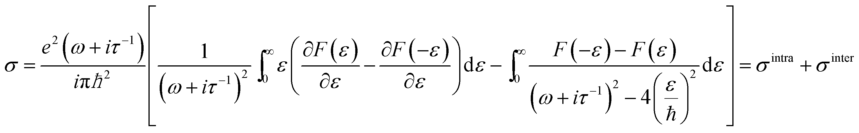
In local limit where spatial dispersion effects are negligible, the surface conductivity of graphene can be obtained from the Kubo formula for finite temperatures T, written as:31
 | (1) |
![[thin space (1/6-em)]](https://www.rsc.org/images/entities/char_2009.gif) 000 cm2 V−1 s−1 is the measured dc mobility, e is the electron charge and vF = 1 × 10⁶ m s−1 is the Fermi velocity.32
000 cm2 V−1 s−1 is the measured dc mobility, e is the electron charge and vF = 1 × 10⁶ m s−1 is the Fermi velocity.32
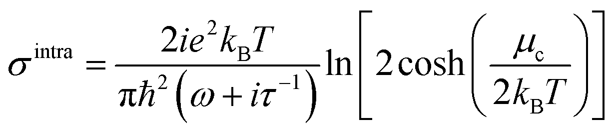
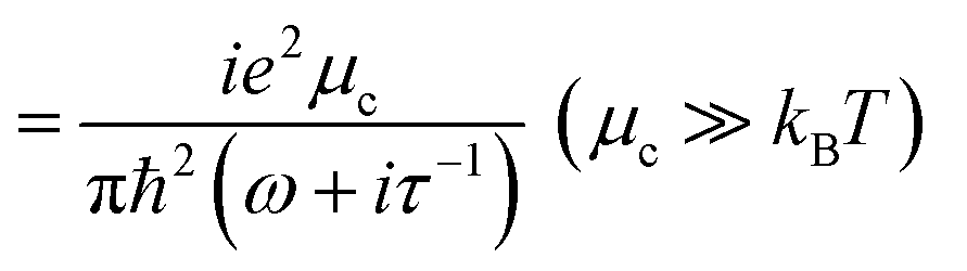
In eqn (1) the first term arises from the contributions of intraband electron–photon scattering and the second term corresponds to contributions from direct interband electron transitions. When μc ≫ kBT (for room temperature, kBT ∼ 26 meV ≪ μc), the term for intraband contribution can be simplified as:
 | (2a) |
 | (2b) |
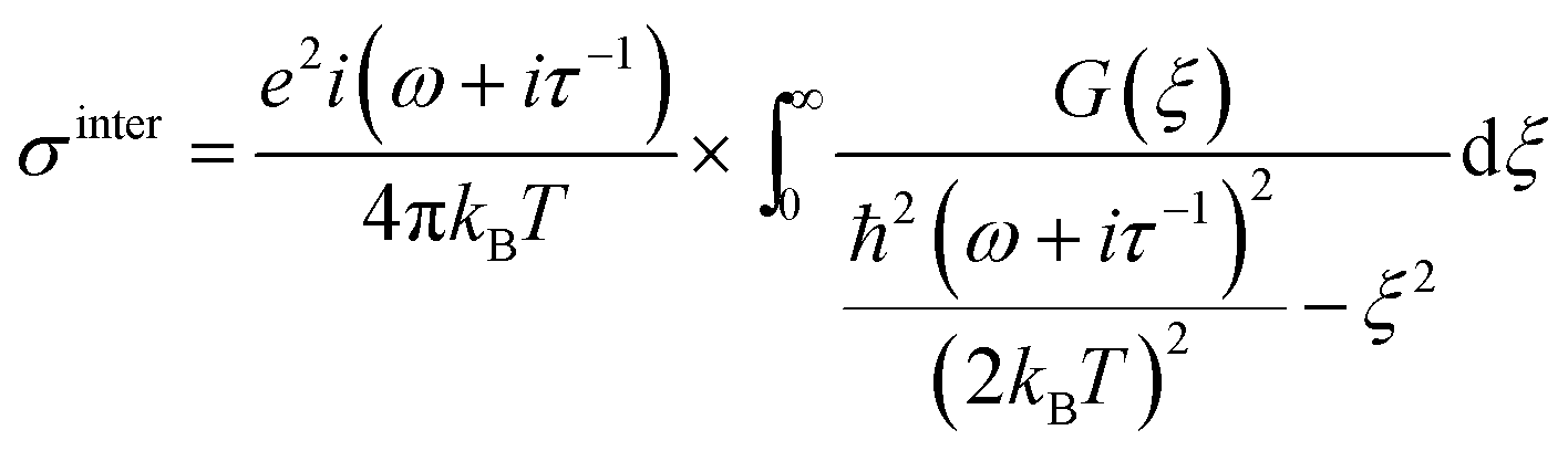
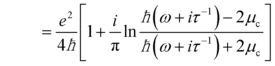
Similarly the inter band contribution can be defined as:
 | (3a) |
 | (3b) |
Eqn (2b) shows that σintra is directly proportional to the chemical potential μc, while eqn (3b) shows that σinter diverges logarithmically when hω ≈ 2μc.
In our simulation, the above surface conductivity cannot be directly used. The volume conductivity can be calculated by σV = σS/Δ, where Δ = Ntg is the thickness of N-layer graphene and tg = 0.34 nm is the monolayer graphene thickness. As graphene is highly anisotropic, only the in-plane component is treated as dispersive. For all our simulation, the graphene is in xz plane and the light emits from the y direction. So the permittivity in different directions could be obtained from the following equations:34
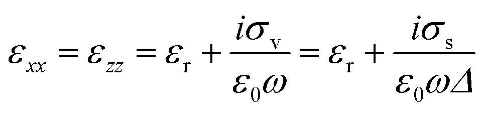 | (4) |
| εyy = εr | (5) |
We studied the permittivity of 5-layer and 10-layer graphene under 850 and 1550 nm wavelengths. Fig. 1 demonstrates the contributions of intraband and interband on permittivity of 5-layer graphene when illuminated with 850 nm and 1550 nm wavelengths. In Fig. 1, the red lines represent the graphene permittivity with 850 nm incident light, while the black ones show the permittivity under 1550 nm light; the dotted lines are contributions from intraband and the dash lines are contributions due to interband, while the solid lines considers both the contribution of interband and intraband. Fig. 1(a) illustrates that in the calculation of the real permittivity of graphene under light of 850 nm and 1550 nm, contributions of both intraband and interband should be considered. The peaks of real permittivity are contributed by intraband, while the contributions of interband are linear. Compared with the peak of graphene real permittivity under 850 nm, the peak of 1550 nm is higher and left shifted. Moreover, the real permittivity of 1550 nm is dominated by intraband at high Fermi level (above the peak value of 0.4 eV). Fig. 1(b) shows that the graphene imaginary permittivity is dominated by interband, and the contributions of intraband could be neglected. At the peak positions of graphene real permittivity (0.73 eV for 850 nm, 0.4 eV for 1550 nm), there are sharp edges in imaginary permittivity. At lower Fermi energies (smaller than 0.4 eV), the graphene imaginary permittivity for 1550 nm is higher than 850 nm.
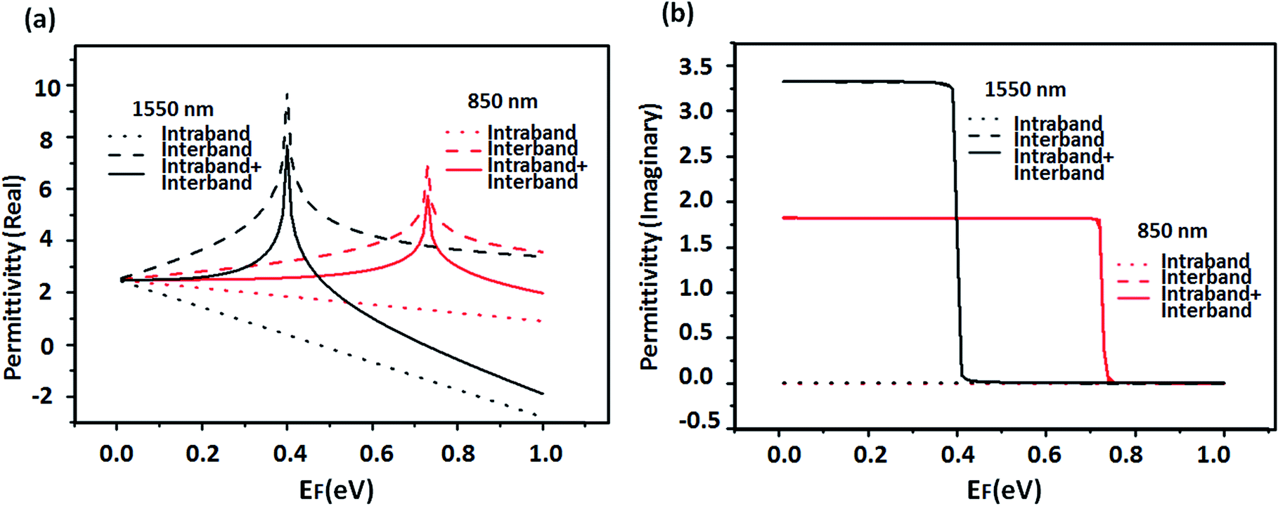 | ||
| Fig. 1 Permittivity of 5-layer graphene for 850 nm and 1550 nm wavelengths with respect to the Fermi level. (a) Real permittivity of graphene considers contributions of intraband (the dotted lines), interband (the dash lines), both intraband and interband (solid lines) (b) imaginary permittivity of graphene considers contributions of intraband (the dotted lines), interband (the dash lines), both intraband and interband (solid lines). | ||
We have also studied the permittivity of 10-layer graphene at 850 nm and 1550 nm wavelengths with respect to Fermi energies. As shown in Fig. 2(a), when shine with the same light, the peaks of graphene real permittivity are at the same positions and the peaks for 10-layer graphene are lower than 5-layer graphene. Fig. 2(b) demonstrates that the imaginary permittivity of graphene with the same light has the same sharp edges. Before the sharp edges, the imaginary permittivity of 5-layer graphene is higher than 10-layer graphene.
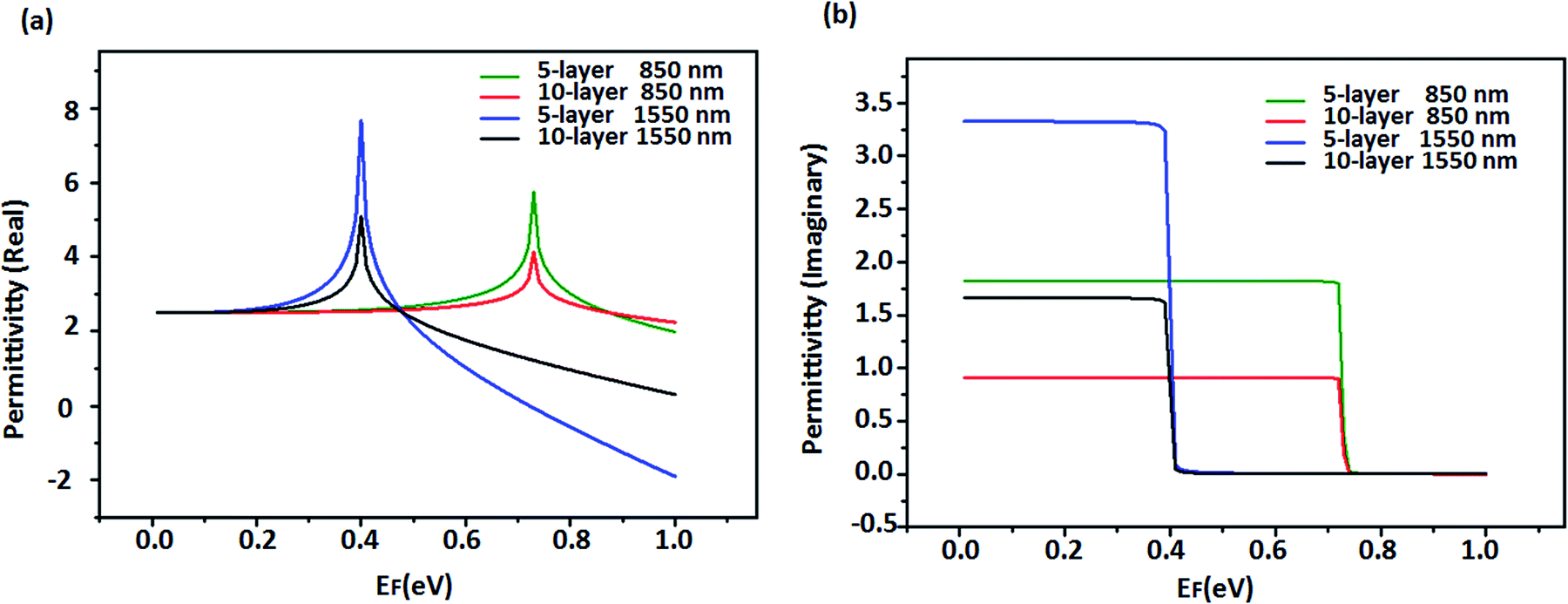 | ||
| Fig. 2 Permittivity of 5-layer and 10-layer graphene under light of 1550 nm and 850 nm. (a) Real permittivity of 5-layer and 10-layer graphene (b) imaginary permittivity of 5-layer and 10-layer graphene. | ||
III. Graphene based ultra-thin Fresnel lenses
The graphene Fresnel zone plate was designed according to the equation:35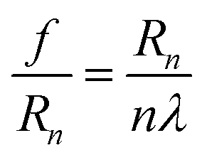 (where λ is the wavelength of light, n = 1, 2, 3…), and the radius of the nth zone (Rn) in a Fresnel lens Rn2 = nR12 (for n > 1). In our simulation R1 = 10 μm, nmax = 23, therefore the diameter of the lens is about 94 μm.
Due to the circular symmetry of the Fresnel zone plates, 2D simulations were performed. The graphene lens was placed on the X plane and the light travelled in the Y direction. Fig. 3(a) shows the computed power flow distribution of the light reflected by the Fresnel lens. The lens was designed from 5-layer graphene at Fermi level 0.73 eV, illuminated with 850 nm wavelength light. The horizontal and vertical cross sectional lines at the focal point are shown in Fig. 3(b) and (c) (red lines), respectively. The simulation confirms the focusing of the reflected light of the graphene-based Fresnel lens. Fig. 3(b) and (c) also show the influence of varying Fermi levels on the lensing effect, while Fig. 3(d) and (e) illustrate the influence of the thickness of graphene on lensing effect.
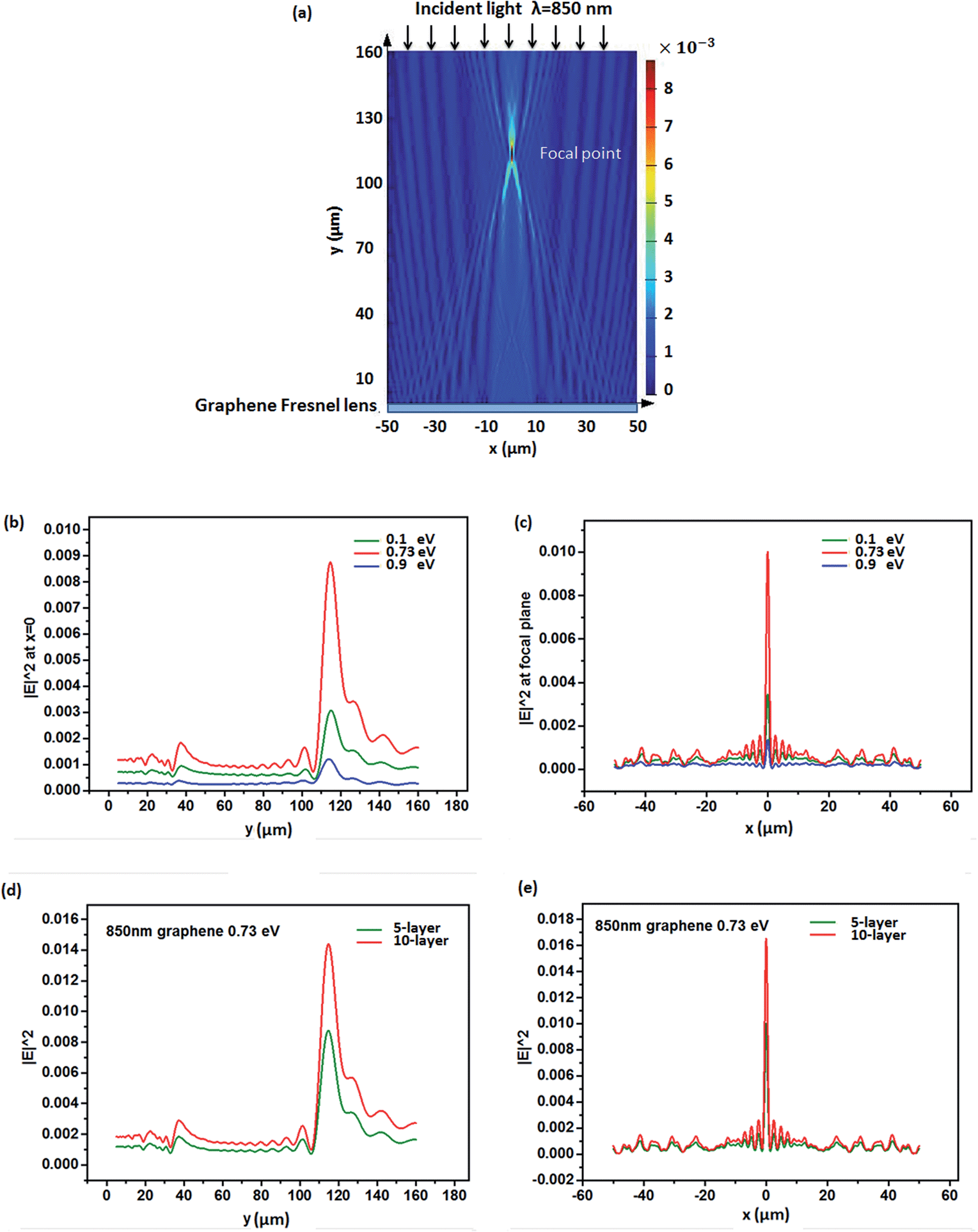 | ||
| Fig. 3 Graphene Fresnel lens illuminated by 850 nm (a) power flow distribution of light reflected from the 5-layer graphene Fresnel lens when illuminated by 850 nm light (Fermi level 0.73 eV). The lens is located at y = 0. (b) Power flow distribution across the y-axis, extracted at x = 0. (c) Power flow distribution across the x-axis, at the focal plane. In (b) and (c), the green, red and blue lines correspond with graphene Fermi levels of 0.1 eV, 0.73 eV and 0.9 eV respectively. Power flow distribution across (d) y-axis and (e) x-axis for 5-layer (green line) and 10-layer (red line) graphene lens. | ||
In Fig. 3(b) and (c), the green lines and blue lines are intensity distribution of cross section lines at focal point when the Fermi level of graphene is 0.1 eV and 0.9 eV, respectively. The focal point power intensity of graphene Fresnel lens with 0.73 eV Fermi level is almost three times as high as that at Fermi level 0.1 eV and nine times as high as that at Fermi level 0.9 eV. This phenomenon is caused by different permittivity of graphene with different Fermi levels, as shown in Fig. 1(a). The focal point intensity of graphene Fresnel lens with 0.73 eV Fermi level is higher due to the high real permittivity (peak) and low imaginary permittivity (almost 0). The focal point intensity of 0.1 eV is higher than 0.9 eV because of higher real and imaginary permittivities. The results show that the focal point intensity can be adjusted by changing graphene's Fermi level which in turn changes the optical properties (dielectric constant and absorption) of the Fresnel zones. The performance of the lens is improved with an increase contrast in the difference of optical properties between the transparent (air) and opaque zones (graphene). Fig. 3(d) and (e) shows that the power intensity at the focal point increases nearly two times when the number of layers increases from 5 to 10, owing to the increased light reflection.
We also studied the influence of different wavelengths on the lensing effect. Fig. 4(a) is the power flow intensity distribution of the reflected light by 5-layer graphene Fresnel lens (Fermi level is the peak value 0.4 eV), illuminated by 1550 nm light. Compared with Fig. 3(a), the focal length in Fig. 4(a) changes from 115 μm (theoretical value for 850 nm is 117.65 μm) to 63.25 μm (theoretical value for 1550 nm should be 64.51 μm). Fig. 4(b) and (c) shows the horizontal and vertical cross sectional lines at the focal point both for 850 nm and 1550 nm light with the same Fermi level (0.1 eV). The focal point intensity of 1550 nm is lower than 850 nm, which means that the graphene Fresnel lens with Fermi level 0.1 eV has imporved lensing effect at 850 nm. This may be attributed to the imaginary permittivity of graphene (Fermi level 0.1 eV) under 1550 nm light that is nearly twice of that under 850 nm light while graphene's real permittivities under both wavelengths are almost same. A higher imaginary permittivity causes losses leading to reduced reflection.
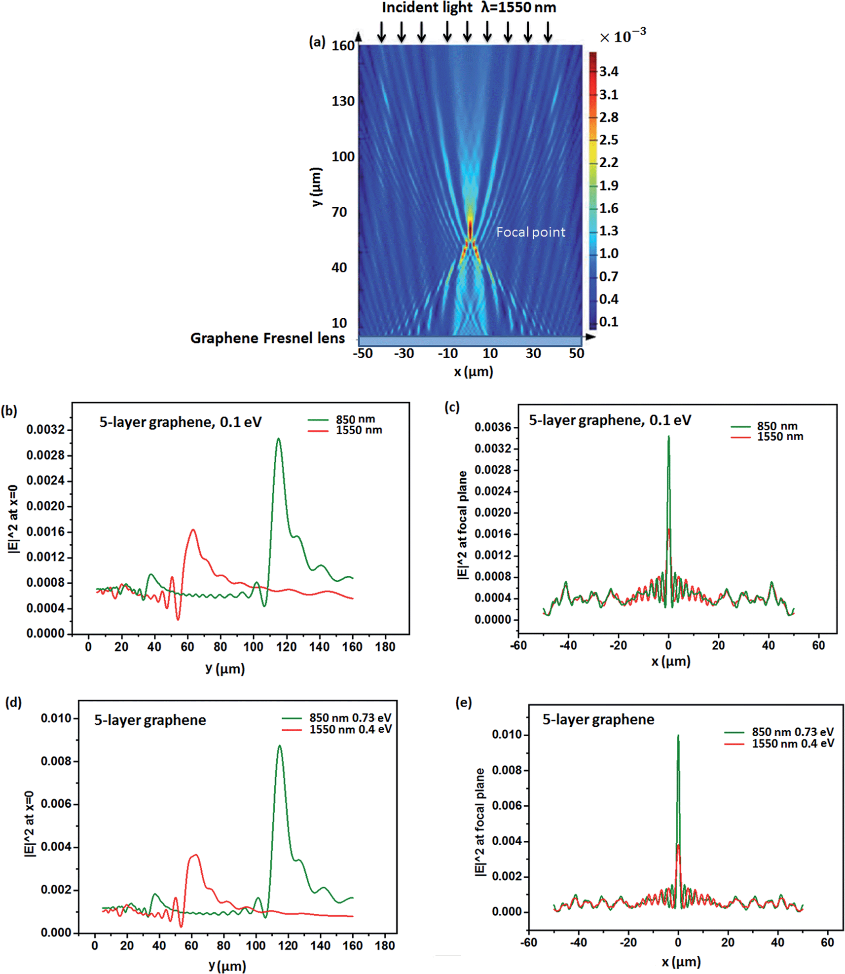 | ||
| Fig. 4 (a) Power flow reflected from 5-layer graphene Fresnel lens when illuminated with light of 1550 nm (Fermi level 0.4 eV), (b) power flow distribution along x = 0, (c) power flow distribution at the focal plane, (d) power flow distribution along x = 0 and (e) the focal plane for lens illuminated by of 850 nm (with Fermi level at peak real permittivity: 0.73 eV) and 1550 nm (with Fermi level at peak real permittivity: 0.4 eV). | ||
Fig. 4(d) and (e) compare the focal intensity distribution when the graphene Fresnel lens is illuminated with 850 nm and 1550 nm light with Fermi levels of peak real permittivities (for 850 nm is 0.73 eV, for 1550 nm is 0.4 eV). The focal point intensity of 1550 nm is lower than 850 nm light. The possible reason could be more absorption related losses due to a higher imaginary permittivity.
IV. Influence of different substrates
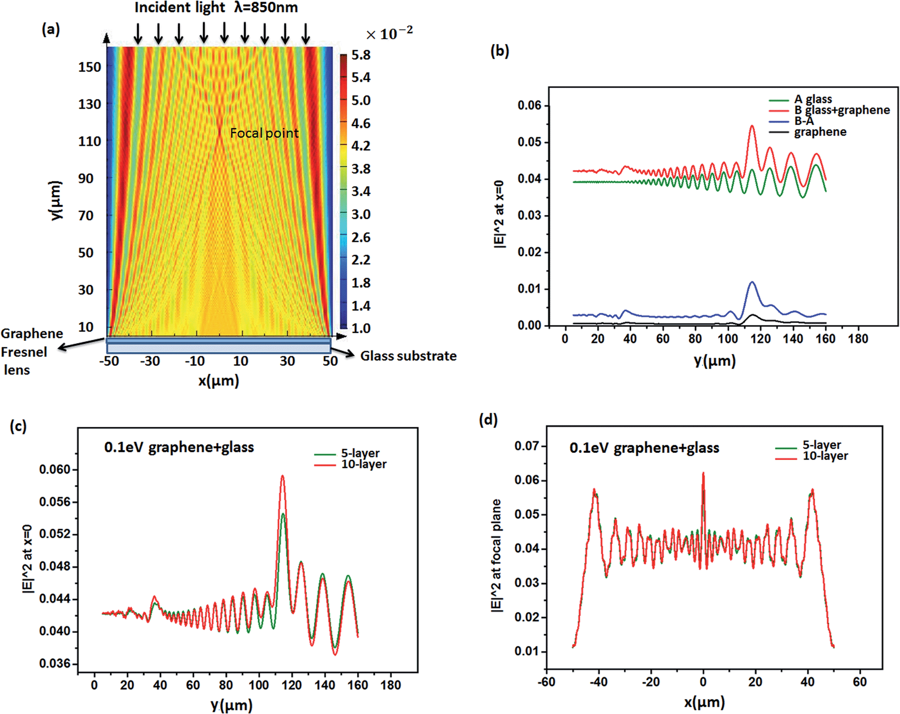
The graphene devices are usually fabricated on various substrates, such as glass and SiO2/Si. Hence we simulate graphene Fresnel lens on these substrates.According to Skulason et al,36 a few-layer graphene on glass could have very high reflection contrast, which could be written as: 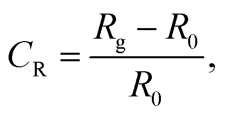 where Rg is reflectance of air–graphene–glass, and R0 is the reflectance of the air–glass interface. This indicates the possibility of fabricating Fresnel lenses on glass.
Fig. 5(a) illustrates the power flow of the reflection of 5-layer graphene Fresnel lens (Fermi level 0.1 eV) on a 5 μm thick glass substrate, illuminated with light of 850 nm wavelength. The focal point is seen from Fig. 5(a), but not as clear as Fig. 3(a). The figure shows an interference pattern produced by the glass substrate.
 | ||
| Fig. 5 Graphene Fresnel lens on glass substrate. (a) Power flow reflected from 5-layer graphene Fresnel lens on glass substrate when illuminated by light of 850 nm (Fermi level 0.1 eV) (b) power flow across y-axis, extracted from x = 0. The green, red and black lines correspond with power flow when light is shined on glass substrate, graphene lens on glass substrate, and on a graphene lens respectively. The blue line is the result of the green line subtracted from the red line. The power flow distribution in across (c) y (at x = 0) and (d) x-axis (at focal point) for 5-layer and 10-layered graphene lens. | ||
Fig. 5(b) compares the intensity distribution along the cross sectional lines at the focal point of graphene Fresnel lens with and without glass substrate. In this figure, the black line shows the intensity distribution of the graphene lens without the substrate, red line shows the distribution for the graphene lens with a glass substrate, and the green line shows the distribution light is shined only on the 5 μm thick glass substrate.
Compared with the black line (graphene Fresnel lens without substrate), it is seen that the wave shape of the red line consists of an interference effect produced by the glass substrate. When the influence of glass is subtracted from the red line we observe a clear focusing effect shown as B-A (blue line) in the figure.
The study of different layered graphene Fresnel lens in Fig. 5(c) and (d) also shows that the interference wave is caused by glass substrate while the focal lensing effect is caused by graphene. Fig. 5(c) and (d) demonstrate that 5-layer and 10-layer graphene Fresnel lenses on glass have comparable interference wave, but 10-layer graphene Fresnel lens will make more contribution to the focal lensing effect, due to the increasing reflection.
The interference effect of the substrates can be explained by the interference theory of light, which is related to the wavelength of incident light as well as the thickness of the substrate. To get the optimized lensing effect, we explore the relationship between the thickness of glass substrate and the reflection of the 5-layer graphene lens/glass structure, with graphene Fermi level 0.73 eV. Fig. 6(a) shows the effective reflection from the graphene Fresnel lens/glass changes when we change the thickness of the glass substrates from 4.3 μm to 5 μm, and the step is 50 nm. In our simulation, the monitor was put on 1 μm above the graphene lens, and the reflection is the total reflected power flow passing the monitor. Periodic change of reflection could be seen from Fig. 6(a), and the period is 300 nm. Theoretically, if there is only a glass substrate, the period should be λ/2 = 425 nm. The difference between the simulation value and the theoretic value may be due to the effect of the 5 layer-graphene Fresnel lens. The shape of the reflection curve is not smooth enough, and this may be caused by the large sweep step.
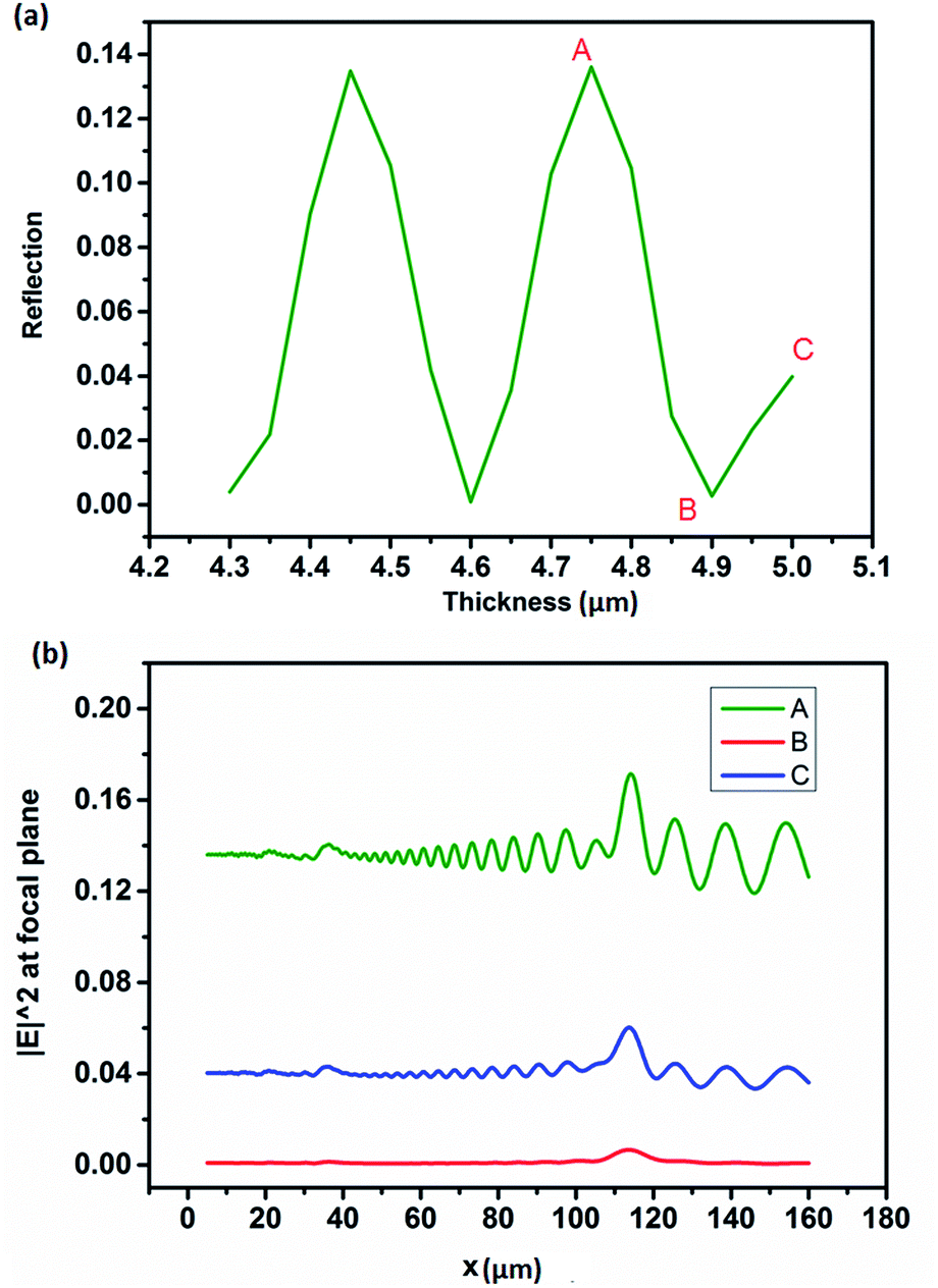 | ||
| Fig. 6 (a) The reflection of 5-layer graphene Fresnel lens on glass substrate with the changing substrate thickness. (b) Power flow distribution along the vertical line across the focal plane. The green, blue and red line represents the power distribution when the substrate thickness equal to points A, B, and C in (a), respectively. | ||
We also choose different thicknesses of substrates to calculate the power distribution along the vertical line across the focal plane, as shown in Fig. 6(b). The green line represents the power distribution of the 4.75 μm thick substrate shown as A in Fig. 6(a). This graph represents the peak reflection caused by the cavity. The red line in Fig. 6(b) is the power distribution with glass substrate thickness at point B (4.9 μm), which has the lowest reflection.
In addition it is reported that graphene has a high optical contrast on the substrate of SiO2/Si, especially when the thickness of SiO2 is 300 nm.37,38 The performance of the graphene Fresnel lens was studied on SiO2/Si substrate. Fig. 7(a) shows the power intensity of reflection from 5-layer graphene Fresnel lens (Fermi level 0.1 eV) on substrate of SiO2/Si substrate, which consists of a 300 nm SiO2 layer and 5 μm Si. Lensing effect can hardly be observed due to the strong interference produced by the substrate. In Fig. 7(b), the power distributions across y-axis are shown for silicon substrate (black line) and silicon substrate with a graphene lens (blue line). The comparison of the two curves shows the light focusing effect produced by the graphene lens. SiO2/Si substrate due to the thin film of SiO2 produces a stronger cavity interference response compared with the glass substrate.
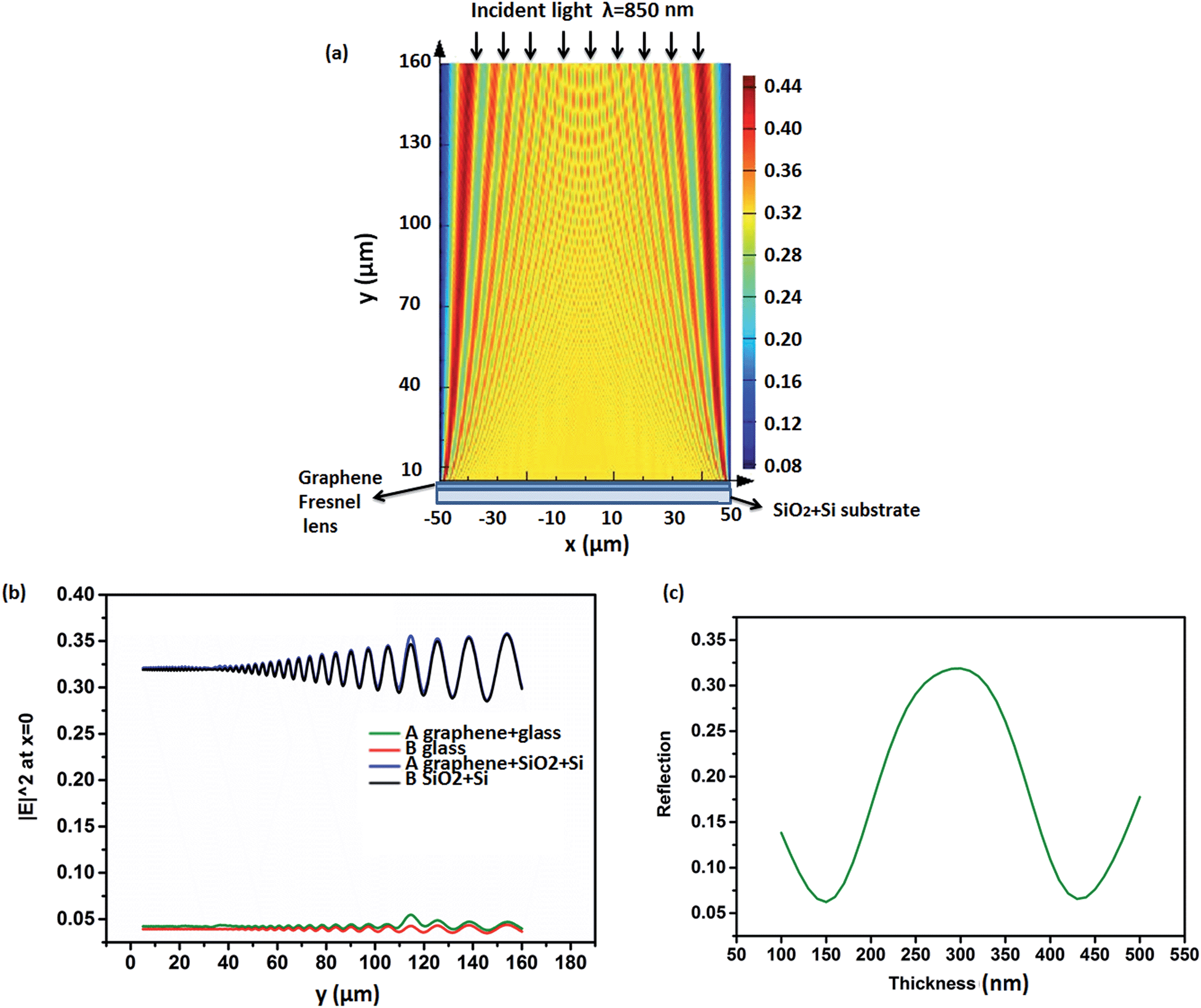 | ||
| Fig. 7 5-layer graphene Fresnel lens (Fermi level 0.1 eV) on SiO2/Si substrate. (a) Power flow reflected from 5-layer graphene Fresnel lens on SiO2/Si substrate (consisting of 300 nm SiO2 layer and 5 μm silicon). (b) Power flow across the y-axis at x = 0. The red and green lines represent the power flow when 850 nm light illuminates a glass substrate and a 5-layer graphene Fresnel lens on glass substrate. The black and blue lines show the power flow when light is projected on a SiO2/Si substrate and a 5-layer graphene lens on SiO2/Si substrate. (c) The reflection of the 5 layer-graphene Fresnel lens on SiO2/Si changes with the thickness of SiO2. | ||
The graphene/SiO2/Si structure could be considered as a sort of Fabry–Perot cavity,39 with graphene acting as the input/output barriers and SiO2 the spacer. According to the principle of Fabry–Perot cavity, the optical contrast of graphene could be adjusted by changing the thickness of spacer or the wavelength of light. We vary the thickness of SiO2 from 100 nm to 500 nm, with increments of 10 nm, and the change of reflection is seen from Fig. 7(c). When the thickness of SiO2 is 300 nm, the graphene/SiO2/Si structure has peak reflection. However, the reflection is very low when the thickness is 150 nm and 440 nm. If we change the thickness of SiO2 for a larger range, the reflection changes periodically and the period is about 300 nm, which is consistent with the results in Fig. 6(a).
V. Conclusions
We have explored the tunable properties of graphene Fresnel lens under illumination of 850 nm and 1550 nm, which are two important wavelengths for optical communication. By adjusting the Fermi level of graphene, the intensity of focal point changes. The properties of graphene on glass and SiO2/Si substrates are also studied. When the incident light is fixed, the thickness of substrates plays a role in producing the interference patterns which affect the focusing ability of the lenses. The results can also be used to explain the properties of other graphene based optical devices using similar substrates.Acknowledgements
The authors thank The Leverhulme Trust for the research funding. Author Contributions: SD performed the work under guidance of HB. AY and KJ helped in writing and proof reading the paper.References
- B. Aničin, V. Babović and D. Davidović, Am. J. Phys., 1989, 57, 312 CrossRef.
- K. Rastani, A. Marrakchi, S. F. Habiby, W. M. Hubbard, H. Gilchrist and R. E. Nahory, Appl. Opt., 1991, 30(11), 1347–1354 CrossRef CAS PubMed.
- M. Ferstl and A.-M. Frisch, J. Mod. Opt., 1996, 43(7), 1451–1462 CrossRef.
- K. Kodate, E. Tokunaga, Y. Tatuno, J. Chen and T. Kamiya, Appl. Opt., 1990, 29(34), 5115–5119 CrossRef CAS PubMed.
- M. Fallahi, K. J. Kasunic, S. Penner, O. Nordman and N. Peyghambarian, Opt. Eng., 1998, 37(4), 1169–1174 CrossRef CAS PubMed.
- B. Morgan, C. M. Waits, J. Krizmanic and R. Ghodssi, J. Microelectromech. Syst., 2004, 13(1), 113–120 CrossRef CAS.
- D. J. D. Carter, D. Gil, R. Menon, M. K. Mondol, H. I. Smith and E. H. Anderson, J. Vac. Sci. Technol., B: Microelectron. Nanometer Struct.--Process., Meas., Phenom., 1999, 17(6), 3449–3452 CrossRef CAS.
- F. Aieta, P. Genevet, M. A. Kats, N. Yu, R. Blanchard, Z. Gaburro and F. Capasso, Nano Lett., 2012, 12(9), 4932–4936 CrossRef CAS PubMed.
- K. S. Novoselov, A. K. Geim, S. Morozov, D. Jiang, Y. Zhang, S. Dubonos, I. Grigorieva and A. Firsov, Science, 2004, 306(5696), 666–669 CrossRef CAS PubMed.
- H. Butt, P. R. Kidambi, B. Dlubak, Y. Montelongo, A. Palani, G. A. Amaratunga, S. Hofmann and T. D. Wilkinson, Adv. Opt. Mater., 2013, 1(11), 869–874 CrossRef.
- C.-F. Chen, C.-H. Park, B. W. Boudouris, J. Horng, B. Geng, C. Girit, A. Zettl, M. F. Crommie, R. A. Segalman and S. G. Louie, Nature, 2011, 471(7340), 617–620 CrossRef CAS PubMed.
- H. Liu, Y. Liu and D. Zhu, J. Mater. Chem., 2011, 21(10), 3335–3345 RSC.
- F. J. García de Abajo, ACS Photonics, 2014, 1(3), 135–152 CrossRef.
- A. E. Nikolaenko, N. Papasimakis, A. Chipouline, F. De Angelis, E. Di Fabrizio and N. I. Zheludev, Opt. Express, 2012, 20(6), 6068–6079 CrossRef CAS PubMed.
- R. Rajasekharan, H. Butt, Q. Dai, T. D. Wilkinson and G. A. Amaratunga, Adv. Mater., 2012, 24(23), OP170–OP173 CrossRef CAS PubMed.
- H. Butt, R. Rajesekharan, Q. Dai, S. Sarfraz, R. Vasant Kumar, G. A. J. Amaratunga and T. D. Wilkinson, Appl. Phys. Lett., 2012, 101, 243116 CrossRef PubMed.
- Q. Zhang, E. H. Hároz, Z. Jin, L. Ren, X. Wang, R. S. Arvidson, A. Lüttge and J. Kono, Nano Lett., 2013, 13(12), 5991–5996 CrossRef CAS PubMed.
- R. H. Baughman, A. A. Zakhidov and W. A. de Heer, Science, 2002, 297(5582), 787–792 CrossRef CAS PubMed.
- A. Andryieuski, A. V. Lavrinenko and D. N. Chigrin, Phys. Rev. B: Condens. Matter Mater. Phys., 2012, 86(12), 121108 CrossRef.
- G. Wang, X. Liu, H. Lu and C. Zeng, Sci. Rep., 2014, 4, 4073 Search PubMed.
- M. Tamagnone, J. Gomez-Diaz, J. R. Mosig and J. Perruisseau-Carrier, Appl. Phys. Lett., 2012, 101(21), 214102 CrossRef PubMed.
- E. Forati, G. W. Hanson, A. B. Yakovlev, A. Alù, arXiv preprint arXiv:1311.4791, 2013.
- A. Majumdar, J. Kim, J. Vuckovic and F. Wang, Nano Lett., 2013, 13(2), 515–518 CrossRef CAS PubMed.
- X. Gan, R.-J. Shiue, Y. Gao, K. F. Mak, X. Yao, L. Li, A. Szep, D. Walker Jr, J. Hone and T. F. Heinz, Nano Lett., 2013, 13(2), 691–696 CrossRef CAS PubMed.
- Q. Bao and K. P. Loh, ACS Nano, 2012, 6(5), 3677–3694 CrossRef CAS PubMed.
- M. Karabiyik, C. Al-Amin, S. Das, N. Pala and W. B. Choi, in Subwavelength, multimode, tunable plasmonic terahertz lenses and detectors, SPIE Defense, security, and sensing, International Society for Optics and Photonics, 2012: pp. 83630L Search PubMed.
- M. Karabiyik, C. Al-Amin and N. Pala, IEEE Trans. Terahertz Sci. Technol., 2013, 3(5), 1–8 CrossRef.
- A. Kuzmenko, E. Van Heumen, F. Carbone and D. Van Der Marel, Phys. Rev. Lett., 2008, 100(11), 117401 CrossRef CAS.
- R. Nair, P. Blake, A. Grigorenko, K. Novoselov, T. Booth, T. Stauber, N. Peres and A. Geim, Science, 2008, 320(5881), 1308–1308 CrossRef CAS PubMed.
- F. Bonaccorso, Z. Sun, T. Hasan and A. Ferrari, Nat. Photonics, 2010, 4(9), 611–622 CrossRef CAS.
- C. H. Gan, H. S. Chu and E. P. Li, Phys. Rev. B: Condens. Matter Mater. Phys., 2012, 85(12), 125431 CrossRef.
- A. Grigorenko, M. Polini and K. Novoselov, Nat. Photonics, 2012, 6(11), 749–758 CrossRef CAS.
- A. Vakil and N. Engheta, Science, 2011, 332(6035), 1291–1294 CrossRef CAS PubMed.
- L. Falkovsky, in Optical properties of graphene, Journal of Physics: Conference Series, IOP Publishing, 2008, p. 012004 Search PubMed.
- Y.-H. Fan, H. Ren and S.-T. Wu, Opt. Express, 2003, 11(23), 3080–3086 CrossRef.
- H. Skulason, P. Gaskell and T. Szkopek, Nanotechnology, 2010, 21(29), 295709 CrossRef CAS PubMed.
- C. Casiraghi, A. Hartschuh, E. Lidorikis, H. Qian, H. Harutyunyan, T. Gokus, K. Novoselov and A. Ferrari, Nano Lett., 2007, 7(9), 2711–2717 CrossRef CAS PubMed.
- P. Blake, E. Hill, A. Castro Neto, K. Novoselov, D. Jiang, R. Yang, T. Booth and A. Geim, Appl. Phys. Lett., 2007, 91(6), 063124 CrossRef PubMed.
- S. Roddaro, P. Pingue, V. Piazza, V. Pellegrini and F. Beltram, Nano Lett., 2007, 7(9), 2707–2710 CrossRef CAS PubMed.
| This journal is © The Royal Society of Chemistry 2014 |