Photocatalytic dye degradation properties of wafer level GaN nanowires by catalytic and self-catalytic approach using chemical vapor deposition

V. Purushothamana, S. Prabhub, K. Jothivenkatachalamb, S. Parthibanc, J. Y. Kwonc and K. Jeganathan*a
aCentre for Nanoscience and Nanotechnology, School of Physics, Bharathidasan University, Tiruchirappalli, 620024, India. E-mail: kjeganathan@yahoo.com; jagan@physics.bdu.ac.in
bDepartment of Chemistry, Anna University, Tiruchirappalli-620024, India
cSchool of Integrated Technology and Yonsei Institute of Convergence Technology, Yonsei University, Yeonsu-gu, Incheon, 406-840, Korea

Received 22nd April 2014 , Accepted 19th May 2014

First published on 19th May 2014


Abstract

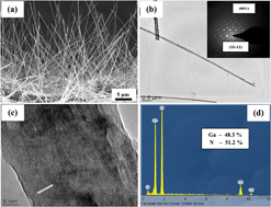
We report the photocatalytic dye degradation properties of self-assembled gallium nitride (GaN) nanowires grown using chemical vapor deposition. GaN nanowires have been fabricated using Ni and Au as the catalyst in addition to the self-catalytic approach. The defect engineered multiband GaN nanowires were subjected to the photocatalytic decay of methylene blue (MB), a common dye in the dying industry, under UV and visible light. Ni-catalyst assisted GaN nanowires possess the maximum degradation of 93% under UV irradiation as correlated with the strong UV band edge emission at 3.42 eV. Interestingly, self-catalytic GaN nanowires show higher photocatalytic activity of 89% under visible irradiation than the catalyst assisted nanowires because of the presence of radiative surface defects in visible region as evidenced by photoluminescence studies. The nanowires exhibit enhanced photocatalytic decay as compared to epitaxial layer due to high surface area and active sites of one-dimensional nanostructures. Detailed analysis further demonstrates the stable photocatalytic activity of the GaN NWs for several cycles against photocorrosion. This work establishes the use of wafer level GaN NWs as a viable photocatalyst for visible light driven decay of organic pollutants.


Introduction

Models of photosynthesis mimetic systems, or artificial photosynthesis systems, including photoelectrochemical water splitting,1 photocatalysis2 and photovoltaic cells,3 have attracted significant amount of attention because of the abundance of availability of solar resource and minimum carbon footprint generated by these systems. Waste water generated by the textile industry contains large amounts of azo dyes, which are considered to be a major threat to the surrounding ecosystem due to their non-biodegradability, toxicity, and potential carcinogenicity. Environmental concerns and the need to meet stringent international standards for waste water safety have encouraged the development of novel, efficient, and low-cost processes for purifying textile aqueous effluents. Azo dye removal by the photoinduced decomposition of pollutants using photocatalysts has been widely studied.4 Semiconductor photocatalysts, especially metal oxides such as TiO2, ZnO, Fe2O3, WO3, etc., have received tremendous attention as photocatalysts because these powders can be easily prepared using simple methods.5–9 However, these photocatalyst nanopowders are generally suspended in water, which limits their practical application because of the difficulty in collecting and recycling photocatalyst powders from a suspension. In order to solve this mobilization problem, immobilized photocatalyst has been suggested by preparing a photocatalytic thin film or nanostructures strongly attached to a substrate.4,10–13 In particular, high density one-dimensional nanostructures are good candidates for photocatalytic applications because photocatalytic activity generally increases with the surface area. Numerous industrial processes require photocatalysts that work under harsh conditions such as high chemical environment with low or high pH. Accordingly, it is very important to synthesize a substrate-supported nanostructured photocatalyst, which is chemically stable under harsh conditions.

Gallium nitride (GaN) is one of the most promising semiconducting materials with a direct band gap of 3.4 eV. Although the wide band gap is a drawback for photocatalytic decay under sunlight, GaN has considerably high flat-band potential (approximately equal to the conduction band edge for n-type conductors of −1.5 eV), which is advantageous because the photogenerated electrons in the conduction band must have high reduction potential. Furthermore, it has been reported that GaN has excellent chemical stability in acidic or basic solutions when compared with the well-known photocatalysts such as TiO2 and ZnO, which makes it very useful in several industrial processes where pollutant degradation under extreme pH conditions is required. In addition, GaN is expected to enable continuous photocatalytic activity and high recyclability without degradation.

In the recent past, semiconductor nanostructures such as nanowires (NWs), nanorods and nanotubes have received a great amount of attention for understanding new structures and utilizing them as a building block for future nanoscale devices.14 Semiconductor NWs have the potential to be used in the fields of electronics,15 optoelectronics,16 photocatalyst17 and sensors18 because of their outstanding electrical, optical, thermal and mechanical properties caused by their size and surface effects. Here, we investigated the photodegradation of methylene blue (MB) under UV and visible light using GaN nanowires grown under various conditions. The higher photocatalytic decay of self-catalyst assisted GaN NWs under visible light is attributed to the defect induced multi-band energy levels in the visible region as evidenced by the optical transitions in PL spectrum.

Experimental methods

A detailed growth process for both the catalytic and self-catalytic approach has already been published elsewhere.19–21 In short, GaN NWs were synthesized by the direct reaction of metal Ga and ammonia (NH3) in the horizontal CVD reactor. Metal Ga of 0.1 g (Alfa Aesar – 99.999%) is taken in a quartz crucible and placed in an alumina boat. A piece of Si (111) (1 × 1 cm2) substrate is cleaned by RCA and placed downstream to the metal Ga. The temperature is kept (@900 °C) constant for all the samples. For catalyst assisted growth, 5 nm thick metal layers (Au and Ni) were deposited by e-beam evaporation method prior to loading into the CVD reactor. N2 and NH3 (99.999%) flow of 500 and 200 SCCM (standard cubic centimetre), respectively are used as carrier and reactant gases. For self-catalytic GaN NWs, initially N2 is flown for 2 min to transport Ga vapours and deposit the Ga droplet layer on the Si substrate, which acts as the catalyst for the subsequent growth of NWs. Then, 200 SCCM of NH3 flow is introduced without the interruption of Ga vapour. The growth duration is fixed for one hour for all the samples. At the end the reactor is turned off to naturally cool down to room temperature.

The morphology and compositional variation of GaN NWs were studied using field emission scanning electron microscopy (FESEM) (Carl Zeiss – Sigma) equipped with energy dispersive X-ray analysis (EDX) (Oxford instruments). EDX was recorded at 10 keV with the point resolution of around 10 nm. High resolution transmission electron microscopy (HRTEM) (JEOL-2010-200 kV) was carried out to examine the crystallinity of a single GaN nanowire. TEM samples were prepared by scratching GaN NWs from the substrate, dispersing them in ethanol, and casting a drop of the suspension on a Cu-grid coated with porous carbon thin film. Photoluminescence (PL) spectrum for the ensemble of NWs were recorded by the He–Cd laser of 325 nm (power: 30 mW) as an excitation source, and the resulting luminescence signal was analyzed by a monochromator (Horiba Jobin Yvon – 0.55 M) using a charge coupled device.

Photocatalytic experiments were performed in an apparatus specially designed for the photocatalytic reaction. The photocatalytic degradation of methylene blue (MB) was chosen to investigate the activity of GaN nanowires because it is one of the important industrial dyes. In a typical experiment, GaN NWs (Fig. S1 in the ESI) on Si substrate (1 × 1 cm2) was suspended inside 50 mL of an aqueous solution containing 10 mg L−1 of MB dye. Prior to irradiation, the suspension was kept in dark for 30 min to attain adsorption–desorption equilibrium by aeration. The photocatalytic activity was investigated under UV and visible light irradiation using 125 W medium pressure mercury lamp emitting at 365 nm (110 μW cm−2, measured by Lutron UV light meter) and 300 W tungsten halogen lamp (8500 lumen), respectively. The distance between the light source and mouth of a glass bottle was 16 cm to reduce the heat radiation from the lamp. The reaction solution was maintained under illumination for 240 min and 180 min for UV and visible light irradiations, respectively. At certain intervals of time, aliquots (1 mL) of the solution were removed and the degradation of MB dye was determined by measuring the maximum absorbance at 554 nm on UV-visible spectrophotometer. The concentration of MB in the solution at various reaction times was determined using a calibration curve of absorbance against standard solutions (10 mM). In order to avoid the photosensitization effect, the entire reaction was carried out under the flow of noble gas (Ar) to remove the degraded gas molecules from the reaction chamber. The percentage of the degradation of MB was calculated by the following equation (eqn (1)).

 
image file: c4ra03642e-t1.tif(1)
where D is the percentage of degradation, A0 and At are initial absorption and absorption at time t, respectively. Photocatalytic degradation of organic compounds usually follows pseudo-first-order kinetics model. The rate constant for the degradation of MB is calculated using the following Langmuir–Hinshelwood kinetic equation.
 
image file: c4ra03642e-t2.tif(2)
where C0 is the initial concentration of the dye solution (mol L−1), C is the concentration of the dye solution at time t (mol L−1), Kapp is the apparent rate constant (min−1). The rate constant for the degradation of MB was calculated from the slope of plot ln(C0/C) vs. irradiation time.

Results and discussion

Fig. 1(a) shows the quasi-aligned GaN NWs grown using the self-catalytic approach having an average diameter and length of ∼160 nm and 10 μm, respectively. Fig. 1(b) shows the TEM image recorded on a single GaN NW that reveals the un-tapered straight NW. Inset of Fig. 1(b) shows the selected area electron diffraction (SAED) pattern recorded on the body of a single NW. Fig. 1(c) shows the HRTEM image of GaN NW, which contains defects such as stacking faults and cubic inclusion. In addition to wurtzite structure, the presence of cubic inclusions and stacking faults is also evidenced by the SAED pattern. Extensive investigations on the HRTEM analysis are warranted to map the defect formation and propagation, which is beyond the scope of this manuscript. EDX recorded on the ensembles of NWs shows (Fig. 1(d)) almost equimolar atomic concentration of Ga and N.
image file: c4ra03642e-f1.tif
Fig. 1 (a) Tilted view FESEM image of self-catalytic GaN NWs; (b) TEM image of GaN NWs. Inset (b) SAED pattern recorded on the body of the NW; (c) HRTEM recorded on the single NW shows defects such as cubic inclusion and (d) EDX recorded on the ensembles of self-catalytic GaN NWs.

Fig. 2(a) shows the Ni-nanodots after annealing a 5 nm thick Ni film coated Si substrate for 15 min at 900 °C under vacuum. Fig. 2(b) shows the tilt-view FESEM image of high yield quasi-aligned Ni-catalyst assisted GaN NWs grown on Si(111) substrates. The average diameter and length of the NWs are ∼120 nm and 10 μm, respectively. EDX recorded (inset of Fig. 2(b)) on the ensembles of GaN NWs shows almost equimolar Ga to N ratio in addition to the presence of other elements such as Ni and substrate impurities of Si and O. The presence of O has been attributed to the presence of strong native oxide of Si substrate. Fig. 2(c) presents a detailed HRTEM examination on the interface between the NW and the catalyst droplet of a single GaN NW, which indicates that the interface is abrupt and smooth. Fig. 2(d) shows that the NW is free of domain boundaries and cubic inclusion with a single-crystalline nature. SAED pattern (inset of Fig. 2(d)) shows that the NW acquired the wurtzite structure and grew along [100].22


image file: c4ra03642e-f2.tif
Fig. 2 (a) Ni-nanodots after annealing the Ni-coated Si substrate for 15 minutes; (b) tilted view FESEM image of Ni-catalyst assisted GaN NWs, inset (b) EDX recorded on the ensembles of the self-catalytic GaN NWs; (c) HRTEM recorded on the interface between the catalyst and body of the NW and (d) HRTEM recorded on the body of a single GaN NW. Inset shows the SAED pattern of single GaN NW.

Fig. 3(a and b) show the FESEM images of Au-catalyst assisted GaN NWs. The average diameter and length of the NWs were 150 nm and 10 μm, respectively. Fig. 3(c) shows that the TEM image recorded on the single nanowire reveals the presence of Au catalyst on the top of the NW. SAED pattern recorded (inset of the Fig. 3(c)) on the NW shows the hexagonal wurtzite crystal structure. Fig. 3(d) shows the HRTEM recorded on the body of a single NW, which reveals that the NWs are free from defects, such as cubic inclusion, and have a single-crystalline nature. The NW diameter is apparently very homogeneous from top to bottom without any tapering effect. The structural qualities of Au-assisted GaN NWs and Ni-assisted GaN NWs are very similar.


image file: c4ra03642e-f3.tif
Fig. 3 (a and b) FESEM images of Au-catalyst assisted GaN NWs; (c) TEM image of single GaN NW, and the corresponding SAED pattern is shown in the inset of (c); and (d) HRTEM recorded on the body of a single GaN NW.

Room temperature photoluminescence (PL) spectrum was recorded on the ensembles of GaN nanowires. Fig. 4(a–c) show the PL spectra for self-catalyst and catalyst assisted GaN NWs. In all the GaN NWs grown under various catalysts, the band edge emission at 3.4 eV dominates the luminescence spectra, which reveal the good optical quality of the GaN NWs. For Ni-catalyst assisted GaN NWs (Fig. 4(c)), in addition to the band edge at 3.43 eV, the broad donor–acceptor pair recombination (DAP) emission is also observed at 3.28 eV. The shallow DAP was attributed to defects such as SiGa and ON because both the defects are quite possible in our growth approach.23 Si has high solubility in both Ni and Au, hence the NWs can have Si interstitials and/or SiGa type defects. Further, it has been widely reported that the catalytically grown GaN NWs on Si substrates can be unintentionally doped with Si. In addition with Si, O could also be incorporated into the growing NW from the complex native oxide layer of Si. The other source for O2 could be from the atmospheric transfer of samples for analysis. There are no other peaks for Ni-catalyst assisted GaN NWs.


image file: c4ra03642e-f4.tif
Fig. 4 Room temperature photoluminescence spectra recorded on the ensembles of (a) self-catalytic GaN NWs, (b) Au-catalyst assisted GaN NWs, (c) Ni-catalyst assisted GaN NWs; and (d) energy level diagram for GaN NW with defect-induced intermediate energy levels and degradation kinetics of MB molecule.

For Au-catalyst assisted GaN NWs (Fig. 4(b)), the band edge is observed at 3.41 eV, which is slightly red shifted from Ni-catalyst assisted NWs. In addition to band edge emission, three other peaks were also clearly resolved from the Lorentzian curve fitting. The peak at 2.98 eV was attributed to the DAP type peak due to defects such as SiGa and ON.24 The peak centered at 3.01 eV can be assigned to the blue luminescence (BL) band of GaN. BL band at room temperature can be attributed to the escape of holes from the acceptor to the valence band, and/or the bound holes may non-radiatively recombine with free electrons in the conduction band. Generally, the BL band is related to a shallow acceptor (SiN or CN) and the origin of this BL band is still a topic of considerable debate in literature.25 The peak at 2.20 eV was attributed to the yellow luminescence (YL) of GaN. In most of the unintentionally and intentionally doped n-type GaN samples grown using the various available techniques, the room-temperature PL spectrum contains YL band centering at 2.10–2.25 eV.

For self-catalytic assisted GaN NWs (Fig. 4(a)) the band edge emission is centered at 3.39 eV, which is 0.3 eV red shifted from Ni-catalyst assisted GaN NWs. In addition to the band edge emission, two additional peaks were also resolved. The BL band is centered at 3.02 eV and the intense YL band is observed at 2.1 eV. The YL band is split into two peaks and its intensity is very dominant and comparable with the band edge emission of GaN. Here, the dominant defect related YL band has been attributed to several defects such as VGa, VN and complex defect-related, which gives rise to emission at 2.1 eV.26 It is also worth noting that both the self-catalytic and Au-catalytic assisted GaN NWs possess considerable defect-related emissions in the visible region, whereas Ni-catalyst assisted GaN NWs does not show any defect-related emissions in the visible region including YL band owing to high optical quality of NWs. The energy level diagram for self-catalytic GaN NW with defect induced intermediate energy levels and degradation kinetics of dye molecule is illustrated in Fig. 4(d).

It is well-known that the dye industry has the problem of disposal of MB dyes due to their high solubility in water. Traces of these dyes are harmful to human beings. MB causes skin diseases and intestinal problems. In view of this, the photocatalytic activity of the prepared GaN NWs for the degradation of MB is demonstrated under UV and visible irradiation. This reaction is chosen because both the electron and hole end up participating in the production of OH radical, which degrades MB and the extent of the reaction can be monitored through optical absorption. We have studied the photocatalytic dye degradation properties for Ni-catalyst assisted GaN NWs, Au-catalyst assisted GaN NWs and self-catalytic GaN NWs. In addition, the results are compared with the MOCVD grown 2 μm thick GaN epitaxial layers. Special care was paid to evaporation losses during illumination. Before the photocatalytic reaction, two separate tubes consisting of (1) GaN NWs immersed in MB solution kept under dark conditions and (2) MB solution without GaN NWs was also kept at UV and visible irradiation. The results show that MB colour remained unaffected in the presence of GaN NWs under dark conditions, and no further photochemical reaction of the dye occurred under UV and visible light in the absence of the GaN NWs. Therefore, both UV-visible illumination and semiconductor catalysts (GaN NWs) are necessary for the efficient decolourization reaction to occur.

Fig. 5(a and b) show the photocatalytic degradation properties of GaN NWs for MB under UV and visible light irradiation with different time durations. UV-vis absorption spectra of degraded MB solution (10 ppm) using as-synthesized GaN NWs is provided in the ESI (Fig. S2 and S3). From UV-vis absorption the concentration of MB in the solution was plotted as a function of irradiation time using Beer–Lambert's law, and the results of different GaN NWs are compared in Fig. 5(c and d). The changes of normalized concentration (C/C0) of MB with irradiation were assumed to be proportional to the normalized maximum absorbance (A/A0).


image file: c4ra03642e-f5.tif
Fig. 5 Photocatalytic dye degradation properties of various GaN NWs and its corresponding efficiency under UV (a and b) and visible light irradiation (c and d).

The Ni-catalyst assisted NWs show the maximum degradation of 93% under UV irradiation for 240 minutes, and the results of the other samples are quite comparable with the Ni-catalyst assisted NWs. However, epitaxial GaN layer grown by MOCVD shows considerable low degradation percentage (∼65%). Here, the results of photocatalytic dye degradation for various GaN NWs cannot be directly compared because the photocatalytic activity depends directly on the surface area of the NWs. However, it is clear that GaN NWs show better photocatalytic activity than their epitaxial counterparts. From the UV absorption spectra, the peak at 662 nm (Fig. S2 and S3 in the ESI) almost disappeared gradually without any considerable shift of the peak position upon UV-light exposure with elapsing time, which indicates a cleavage of the aromatic ring of the dye molecule.

Surprisingly, photodegradation activity of GaN NWs increases under visible light irradiation and the maximum degradation of 89% for the self-catalytic GaN NWs was achieved within 180 minutes. It is very important to note that Ni-catalyst assisted NWs show better performance for photocatalytic degradation under UV light. However, in case of visible light the trend reverses and the photocatalytic degradation of self-catalytic GaN NWs shows better degradation activity. These results can be understood by correlating the photocatalytic dye degradation property with the optical transitions in PL spectra.

In general, the organic waste degradation is due to the oxidation by the photo generated carriers. Electrons generated in semiconductors during light irradiation contribute to reductions whose potentials are positioned between the conduction and valence bands, and the band gap of GaN possesses all the possible redox potentials.27 It is well-known that holes are responsible for oxidation and electrons are responsible for reduction.28 We believe that electrons from the energy levels of surface defects, such as vacancies, produce excessive electron–hole recombination process. PL spectrum of self-catalytic GaN NWs shows the band edge emission at 3.42 eV in addition with the broad BL and YL band at 3.01 eV and 2.2 eV due to defect-induced transitions. The spectrum encompasses the most visible region of the solar spectrum including UV-optical band edge emission for self-catalytic and Au-catalytic NWs. The samples dominant with the visible emission undergo efficient photocatalytic decay of dyes in a short duration. Under visible irradiation, sample produces high density electron–hole pairs on the surface of NWs, which promotes decay of dyes due to oxidation because the energy level matches with the redox potential of GaN with the organic pollutants (Fig. 4(d)). The samples with high defect concentration including high non-radiative defects as well as high shallow donor concentration have been reported to exhibit low photocatalytic activity.29 In general, the non-radiative point defects include the recombination of electron–hole pairs via thermally remitting any optical emissions. These defects do not contribute to the photo decay process thereby reducing efficiency. The radiative type defects-induced BL and YL bands in self-catalytic and Au-catalytic assisted NWs are optically active in the solar spectrum, which is commensurate with the enhancement of degradation under visible light.

It is also possible to compare the luminescence intensity for various GaN NW samples and their corresponding photocatalytic dye degradation activity. Although the optical intensity directly depends on the density of NWs, the defects-related intensity can be well compared with its own band edge. From this perspective, self-catalytic GaN NWs show that YL band emission is comparable with the band edge emission. The BL band and YL band emissions are in the visible region and band edge emission is at the UV range. Hence, the higher photocatalytic activity of self-catalytic GaN NWs under visible region could be well triggered from the radiative type defects. For Ni-catalyst assisted GaN NWs, there are no visible BL and YL bands, which corroborates the lower photocatalytic degradation under visible region, while it demonstrated the maximum degradation of 93% under UV irradiation due to the dominant band edge at 363 nm.

GaN nanowires also have favorable reuse performance, which has been demonstrated by five successive recycling tests for photocatalytic reduction of MB. As shown in Fig. 6, the nanowires exhibit almost no deactivation during five cycles of photoactivity test for the reduction of MB under visible light irradiation. The decay conversion efficiency of MB is nearly constant for each run. Therefore, the GaN nanowires can perform as stable visible light driven photocatalyst towards the selective reduction of azo dye compounds, such as MB, at room temperature under ambient atmosphere.


image file: c4ra03642e-f6.tif
Fig. 6 Reusability of GaN nanowires under visible light irradiation (a) Ni-catalyst assisted NWs, (b) Au-catalyst assisted NWs and (c) self-catalytic NWs. It clearly shows that the dye degradation efficiency of the nanowires does not reduce even after the 5 cycles of usage.

Conclusion

The photocatalytic activity of wafer level GaN NWs grown under catalytic and self-catalytic approach was investigated for the degradation of emergent organic pollutant dye MB under UV and visible light irradiation. The self-catalyst assisted GaN NWs exhibit the high photocatalytic decay of 89% under visible light while Ni-catalyst assisted GaN NWs decay 93% under UV irradiation. The higher photocatalytic activity of Ni-catalyst assisted GaN NWs under UV irradiation was attributed to the dominant band edge emission at UV region. The optically active radiative defects in the visible region are responsible for the enhanced photocatalytic activity of self-catalytic GaN NWs under visible light. The defect-engineered visible emission actively participates in the photocatalytic decay of dyes under solar spectrum, and the results well corroborate with the room temperature photoluminescence emissions.

Acknowledgements

K.J. thanks the Department of Science and Technology (DST), Govt. of India for financial assistances under the Nanomission project no. SR/NM/NS-77/2008. V.P. acknowledges CSIR, India for the award of senior research fellowship.

References

  1. Z. Zou, J. Ye, K. Sayama and H. Arakawa, Direct splitting of water under visible light irradiation with an oxide semiconductor photocatalyst, Nature, 2001, 414, 625–627 CrossRef PubMed.
  2. A. Mills, R. H. Davies and D. Worsley, Water purification by semiconductor photocatalysis, Chem. Soc. Rev., 1993, 22, 417–425 RSC.
  3. M. Grätzel, Dye-sensitized solar cells, J. Photochem. Photobiol., C, 2003, 4, 145–153 CrossRef.
  4. K. Vinodgopal and P. V. Kamat, Enhanced Rates of Photocatalytic Degradation of an Azo Dye Using SnO2/TiO2 Coupled Semiconductor Thin Films, Environmental Science & Technology, 1995, 29, 841–845 Search PubMed.
  5. T. Wu, G. Liu, J. Zhao, H. Hidaka and N. Serpone, Photoassisted Degradation of Dye Pollutants. Self-Photosensitized Oxidative Transformation of Rhodamine B under Visible Light Irradiation in Aqueous TiO2 Dispersions, J. Phys. Chem. B, 1998, 102, 5845–5851 CrossRef.
  6. S. Chakrabarti and B. K. Dutta, Photocatalytic degradation of model textile dyes in wastewater using ZnO as semiconductor catalyst, J. Hazard. Mater., 2004, 112, 269–278 CrossRef PubMed.
  7. S. Sakthivel, B. Neppolian, M. V. Shankar, B. Arabindoo, M. Palanichamy and V. Murugesan, Solar photocatalytic degradation of azo dye: comparison of photocatalytic efficiency of ZnO and TiO2, Sol. Energy Mater. Sol. Cells, 2003, 77, 65–82 CrossRef.
  8. M. Shen, X. Zhang, K. Dai, H. Chen and T. Peng, Hierarchical PbMoO4 microspheres: hydrothermal synthesis, formation mechanism and photocatalytic properties, CrystEngComm, 2013, 15, 1146–1152 RSC.
  9. K. Dai, Y. Yao, H. Liu, I. Mohamed and H. Chen, Enhancing the photocatalytic activity of lead molybdate by modifying with fullerene, J. Mol. Catal. A: Chem., 2013, 374–375, 111–117 CrossRef PubMed.
  10. C. Liu, H. Chen, K. Dai, A. Xue, H. Chen and Q. Huang, Synthesis, characterization, and its photocatalytic activity of double-walled carbon nanotubes–TiO2 hybrid, Mater. Res. Bull., 2013, 48, 1499–1505 CrossRef PubMed.
  11. K. Dai, H. Chen, T. Peng, D. Ke and H. Yi, Photocatalytic degradation of methyl orange in aqueous suspension of mesoporous titania nanoparticles, Chemosphere, 2007, 69, 1361–1367 CrossRef PubMed.
  12. K. Dai, T. Peng, D. Ke and B. Wei, Photocatalytic hydrogen generation using a nanocomposite of multi-walled carbon nanotubes and TiO2 nanoparticles under visible light irradiation, Nanotechnology, 2009, 20, 125603 CrossRef PubMed.
  13. K. Dai, X. Zhang, K. Fan, T. Peng and B. Wei, Hydrothermal synthesis of single-walled carbon nanotube–TiO2 hybrid and its photocatalytic activity, Appl. Surf. Sci., 2013, 270, 238–244 CrossRef PubMed.
  14. J. C. Johnson, H. J. Choi, K. P. Knutsen, R. D. Schaller, P. Yang and R. J. Saykally, Single gallium nitride nanowire lasers, Nat. Mater., 2002, 1(2), 106–110 CrossRef PubMed.
  15. P. D. Ye, B. Yang, K. K. Ng, J. Bude, G. D. Wilk, S. Halder and J. C. M. Hwang, GaN metal-oxide-semiconductor high-electron-mobility-transistor with atomic layer deposited Al2O3 as gate dielectric, Appl. Phys. Lett., 2005, 86, 063501 CrossRef PubMed.
  16. C. J. Barrelet, A. B. Greytak and C. M. Lieber, Nanowire Photonic Circuit Elements, Nano Lett., 2004, 4(10), 1981–1985 CrossRef.
  17. J. L. Yang, S. J. An, W. I. Park, G. C. Yi and W. Choi, Photocatalysis Using ZnO Thin Films and Nanoneedles Grown by Metal–Organic Chemical Vapor Deposition, Advanced Materials, 2004, 16(18), 1661–1664 CrossRef.
  18. Y. S. Kim, I. S. Hwang, S. J. Kim, C. Y. Lee and J. H. Lee, CuO nanowire gas sensors for air quality control in automotive cabin, Sens. Actuators, B, 2008, 135, 298–303 CrossRef PubMed.
  19. V. Purushothaman and K. Jeganathan, Structural Evolution and Growth Mechanism of Self-Assembled Wurtzite Gallium Nitride (GaN) Nanostructures by Chemical Vapor Deposition, J. Phys. Chem. C, 2013, 117, 7348–7357 Search PubMed.
  20. V. Purushothaman, V. Ramakrishnan and K. Jeganathan, Whiskered GaN nanowires by self-induced VLS approach using chemical vapor deposition, CrystEngComm, 2012, 14, 8390–8395 RSC.
  21. V. Purushothaman, V. Ramakrishnan and K. Jeganathan, Interplay of VLS and VS growth mechanism for GaN nanowires by a self-catalytic Approach, RSC Adv., 2012, 2, 4802 RSC.
  22. X. Duan and C. M. Lieber, Laser-Assisted Catalytic Growth of Single Crystal GaN Nanowires, J. Am. Chem. Soc., 1999, 122, 188–189 CrossRef.
  23. A. Soudi, E. H. Khan, J. T. Dickinson and Y. Gu, Observation of Unintentionally Incorporated Nitrogen-Related Complexes in ZnO and GaN Nanowires, Nano Lett., 2009, 9(5), 1844–1849 CrossRef PubMed.
  24. J. Liu, X. M. Meng, Y. Jiang, C. S. Lee, I. Bello and S. T. Lee, Gallium nitride nanowires doped with silicon, Appl. Phys. Lett., 2003, 83, 4241–4243 CrossRef PubMed.
  25. M. A. Reshchikov and H. Morkoç, Luminescence properties of defects in GaN, J. Appl. Phys., 2005, 97, 061301 CrossRef PubMed.
  26. N. Thillosen, K. Sebald, H. Hardtdegen, R. Meijers, R. Calarco, S. Montanari, N. Kaluza, J. Gutowski and H. Lüth, The State of Strain in Single GaN Nanocolumns As Derived from Micro-Photoluminescence Measurements, Nano Lett., 2006, 6, 704–708 CrossRef PubMed.
  27. H. S. Jung, Y. J. Hong, Y. Li, J. Cho, Y. J. Kim and G. C. Yi, Photocatalysis Using GaN Nanowires, ACS Nano, 2008, 2, 637–642 CrossRef PubMed.
  28. B. Liu, A. Khare and E. S. Aydil, TiO2–B/Anatase Core–Shell Heterojunction Nanowires for Photocatalysis, ACS Appl. Mater. Interfaces, 2011, 3, 4444–4450 Search PubMed.
  29. F. Liu, Y. H. Leung, A. B. Djurišić, A. M. C. Ng and W. K. Chan, Native Defects in ZnO: Effect on Dye Adsorption and Photocatalytic Degradation, J. Phys. Chem. C, 2013, 117, 12218–12228 Search PubMed.

Footnote

Electronic supplementary information (ESI) available. See DOI: 10.1039/c4ra03642e

This journal is © The Royal Society of Chemistry 2014
Click here to see how this site uses Cookies. View our privacy policy here.