Electronic structure engineering in chemically modified ultrathin ZnO nanofilms via a built-in heterointerface†
Hongyan Guoab,
Ning Lucd,
Jun Daid,
Xiao Cheng Zengbd,
Xiaojun Wu*abe and
Jinlong Yangbe
aCAS Key Laboratory of Materials for Energy Conversion and Department of Materials Science and Engineering, Hefei, Anhui 230026, China. E-mail: xjwu@ustc.edu.cn
bSchool of Chemistry and Materials Science and Hefei National Laboratory of Physical Science at the Microscale, University of Science and Technology of China, Hefei, Anhui 230026, China
cCenter for Nano Science and Technology, Department of Physics, Anhui Normal University, Wuhu, Anhui 241000, China
dDepartment of Chemistry and Nebraska Center for Materials and Nanoscience, University of Science and Technology of China, Hefei, Anhui 230026, China
eSynergetic Innovation Center of Quantum Information & Quantum Physics, University of Science and Technology of China, Hefei, Anhui 230026, China
First published on 9th April 2014
Abstract
Zinc oxide, a typical semiconducting material crystallizing in either hexagonal wurtzite or cubic zinc blende structure in the bulk, exhibits a graphite-like structure in ultrathin nanofilms with a few layers. On the basis of first-principles calculations, we show that the ultrathin ZnO nanofilms regain their bulk structures with either surface hydrogenation or fluorination. In particular, a heterointerface containing only Zn–Zn or O–O bonds can be built spontaneously in ultrathin ZnO nanofilms depending on their surface chemical modification, dividing the nanofilm into two different domains. An extended impurity state, constrained in the heterointerface, is created around the Fermi energy level. The ZnO nanofilms with a Zn–Zn heterointerface are metallic, whereas those with an O–O heterointerface are still semiconducting. The built-in heterointerface presents a novel channel for charge collection and transport in ZnO nanofilms for their potential applications in electronic and optoelectronic devices.
Introduction
Zinc oxide is an important metal oxide semiconductor material with a wide band gap (about 3.3 eV),1 large exciton binding energy (60 meV), and extraordinary piezoelectric and optical properties.2 These unusual properties give ZnO wide applications in UV-light emitting diodes,3 solar cells,4 photocatalysts, etc.5 Although crystalline in wurtzite or cubic zincblende structures in the bulk, ZnO material can exhibit various morphologies at the nanoscale, such as nanofilms,6–8 nanowires,9 nanoclusters,10 nanobelts,11 and nanotubes,12 nanorods,13 nanonails,14 and nanorings.15 In particular, the wurtzite-type ZnO nanofilms prefer a graphite-like structure when the number of ZnO (0001) layers is reduced due to the depolarization of the surfaces.16–18 Notably, polar oxide surfaces of compound semiconductors are electrostatic unstable due to the presence of this macroscopic dipole, which can be compensated by modification of charge density or at a critical film thickness which is a new compensation mechanism.19–26 The energetically preferred growth direction of ZnO is the (0001) axis, along which Zn and O planes alternate in a regular fashion. Experimentally, Tushce et al. have successfully synthesized two-monolayer-thick depolarized ZnO (0001) films deposited on Ag (111) surface, where Zn and O atoms are arranged in planar sheet like in the hexagonal boron-nitride (h-BN) monolayer.22 The graphene-like ZnO monolayer is predicted to be a semiconductor with a wide band gap of 3.57 eV with GW method.27 Further calculations have also shown that the half-metallicity may be induced in ZnO monolayer by introducing Zn vacancy, doping with metal or nonmetal element, or chemically modifying with H, F, or NH2.28–33Recently, experiments and theoretical calculations have revealed that few layers of two dimensional materials, such as graphene, h-BN, and ZnO monolayers, can transformed into ultrathin nanofilms with covalent bonds between layers by chemical functionalization. For instance, graphene multilayers can be converted into ultrathin diamond (111) nanofilms by surface modification, which exhibit large band gap independent of their thickness. Similarly, theoretical work predicted that both diamond-like and cubic boron-nitride nanofilms with tunable band gap and magnetism can be obtained by chemically modifying h-BN multilayer.34 Tang et al. recently showed that the wurtzite-type ultrathin ZnO films can also be formed and stabilized with the hydrogenation of ZnO bilayer or trilayer.35 Moreover, the half-metallicity was predicted in ultrathin ZnO nanofilms with semihydrogenation for their applications in spintronics.
In this work, we show that the heterointerface with only Zn–Zn or O–O bonds can be formed spontaneously in diamond-like ZnO nanofilms when hydrogenating or fluorinating ZnO multilayer. The heterointerface divides ZnO nanofilms into two domains. In particular, contrary to the intrinsic semiconducting property of ZnO bulk, the ZnO nanofilms with heterointerface can be either metallic or semiconducting with an extended impurity state constrained at the heterointerface. Our studies present a new design of ZnO nanofilms with embedded metallic heterointerface for their applications in energy conversion and electronics.
Computational methods
All calculations are performed within the framework of spin-polarized plane-wave density functional theory (DFT), implemented in the Vienna ab initio simulation package (VASP).36,37 The generalized gradient approximation (GGA) with the Perdew–Burke–Ernzerhof (PBE) functional and projector augmented wave (PAW) potentials are used.38–40 We adopted a unit cell for the investigation and a test calculation with a 2 × 2 supercell yields nearly the same results. The vacuum size is larger than 15 Å between two adjacent images. In ZnO bilayer with AB (AA) stacking between two layers, we let the Zn (Zn/O) atom of one layer directly above the O (Zn/O) atom of the other layer. An energy cutoff of 400 eV is used for the plane-wave expansion of the electronic wave function. Geometry structures are relaxed until the force on each atom is less than 0.01 eV Å−1, and the convergence criteria for energy 1 × 10⁻⁵ eV is met. The two dimensional Brillouin zone integration using Γ-center scheme is sampled with 9 × 9 × 1 grid for geometry optimizations and 15 × 15 × 1 grid for static electronic structure calculations. The lattice parameters were optimized for each system. Note that PBE method always underestimated the band gap of semiconductor, the screen hybrid HSE06 method is used to check the band structures.41,42Results and discussions
At first, the benchmark calculations were performed on the pure ZnO monolayer. The fully relaxed ZnO monolayer presents a graphene-like planar structure with Zn–O bond length of about 1.90 Å. The electronic structure calculation indicates that the graphene-like ZnO monolayer is a nonmagnetic (NM) semiconductor with a direct band gap of about 1.66 eV at the Γ point of the first Brillouin zone, consistent well with previous theoretical calculations.43–45 Note that the DFT always underestimated the band gap of semiconductor. The formation energy difference between ZnO bulk and ZnO monolayer is 0.46 eV per ZnO pair, where ZnO monolayer is energetically unfavorable. Nevertheless, the ZnO monolayer can be realized in experiment.17 Due to the ionicity of Zn–O bond in ZnO monolayer, the adsorption of H and F atom on ZnO monolayer is site-selective. The adsorption energy is defined as Eads = E(H/F adsorbed ZnO sheet) − E(H/F) − E(ZnO sheet), where E(system) is the total energy of system. The calculated adsorption energy indicates that the H atom prefers to adsorb on the top site of O oxygen atom with the adsorption energy of 1.65 eV. The adsorption energy on the top of Zn atom is only 0.30 eV. The optimized O–H and Zn–H bond lengths are 0.98 and 2.12 Å, respectively. Differently, the F atom prefers to adsorb on the hollow site of ZnO monolayer with the total adsorption energy of about 2.30 eV. The optimized F–Zn and F–O bond lengths are 2.11 and 2.01 Å, respectively.AB-stacked ZnO bilayer
Upon the graphene-like ZnO bilayer, there are two possible stacking configurations, i.e. AB or AA stacking. Fig. 1(a) displays the optimized structures and electronic band structures of AB-stacked ZnO bilayer. The interlayer distance is 2.43 Å and AB-stacked ZnO bilayer is nonmagnetic semiconductor with a direct band gap of 1.45 eV at Γ point, consistent with previous theoretical calculations.28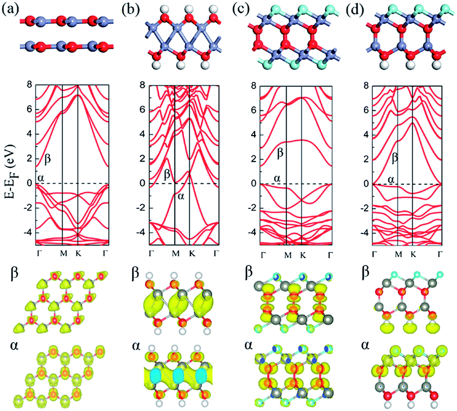 | ||
| Fig. 1 The optimized structures and the calculated band structures of (a) pure, (b) hydrogenated, (c) fluorinated and (d) H and F co-adsorbed ZnO bilayer with AB stacking. The red, grey, white and blue balls represent O, Zn, H and F atoms, respectively. The Fermi level is marked by a dashed line. The bellow in (b) is the partial charge density distribution of the α and β bands crossing the Fermi level. The bellow in (a), (c) and (d) is partial charge density distribution of the corresponding α and β bands, respectively. The isosurface value is 0.01 e Å−3. | ||
As shown in Fig. 1(b), different from the perfect AB-stacked ZnO bilayer, the hydrogenation of AB-stacked ZnO bilayer's surfaces induce a spontaneous binding of Zn atoms between two layers and a heterointerface with only Zn–Zn bonds is formed. Note that H atom prefers chemically adsorb on the top site of O atom. Each Zn atoms forms three Zn–Zn bonds with neighboring three Zn atoms in the neighboring layer and two ZnO layers still keep their AB stacking. The optimized bond lengths of Zn–O, Zn–Zn, and O–H are 2.12, 2.75 and 0.98 Å, respectively. As shown in Fig. 1(b), the calculated band structure indicates that hydrogenated ZnO bilayer is metallic. Two bands (labeled with α and β) cross the Fermi energy level with large dispersion. The bellow in Fig. 1(b) shows that the charge density of the extended α and β bands are mainly contributed by Zn atoms in the heterointerface. Test calculation with the screened hybrid HSE06 functional confirms the metallicity of hydrogenated ZnO bilayer with AB stacking (see Fig. S1(b)†). To further investigate the stability of the hydrogenated ZnO bilayer with Zn–Zn heterointerface, we calculated the interaction energy between two ZnO sheet with or without hydrogenation. The interaction energy is defined as EIE = Eup + Edown − Ebilayer, where Eup is the total energy of up ZnO layer with or without H/F adsorption, Edown is the total energy of down ZnO layer with or without H/F adsorption, Ebilayer is the total energy of ZnO bilayer with or without H/F adsorption. For the pure ZnO bilayer with AB stacking, the interaction between two ZnO sheets is van der Waals interaction and the calculated interaction energy is as low as about 0.29 eV. Note that the weak interaction can't be described accurately with pure DFT calculations and DFT method with dispersion calculation may present improved results on binding energy. The hydrogenation of ZnO bilayer's surface definitely strengthens this interaction via forming Zn–Zn chemical bonds. The calculated interaction energy between two ZnO sheets in hydrogenated ZnO bilayer is about 1.23 eV per supercell, indicating the forming Zn–Zn heterointerface has high thermal stability.
Differently, the fluorination of AB-stacked ZnO bilayer leads to the spontaneous formation of O–O heterointerface in ZnO bilayer, as shown in Fig. 1(c). F atoms adsorbed on the hollow site of ZnO hexagon rings and pulls out three Zn atoms from its original planar. The average bond length of Zn–F bonds is 2.09 Å and the O–O bond length in heterointerface is 1.48 Å. The calculated interaction energy between two ZnO sheets in fluorinated ZnO bilayer is 2.01 eV, which is larger than that in the hydrogenated ZnO bilayer with AB stacking. The calculated electronic structure shows that the fluorinated ZnO bilayer is a semiconductor with a direct band gap of 1.50 eV, as shown in Fig. 1(c), which is slightly larger than that of pure ZnO bilayer (1.45 eV). The partial charge density analysis shows that the highest valence band (α) mainly comes from the p orbital of the O atoms in the interface, and Zn's d and F's p orbitals have minor contributions. The lowest conduction band (β) is also mainly contributed by the p orbital of the O atoms in the heterointerface, and the s orbital of the O atoms in the interface and F's p orbital have minor contributions, as shown in the bellow of Fig. 1(c).
As a comparison, the AB-stacked ZnO bilayer with both hydrogenated and fluorinated surfaces are considered, as shown in Fig. 1(d). The hybrid hydrogenation and fluorination on both surfaces of AB-staked ZnO bilayer leads to the formation of Zn–O bonding between two ZnO monolayers, recovering its bulk structure. The Zn–F, Zn–O, and O–H bond lengths are 2.10, 1.81, and 0.98 Å, respectively. The calculated interaction energy between two ZnO layers is 4.78 eV per supercell, revealing that the bulk-like Zn–O connected ZnO bilayer is the most stable configuration. Notably, the bulk-like ZnO bilayer with both hydrogenation and fluorination is a semi-metal. However, the hybrid HSE06 result (see Fig. S1(d)†) shows that it is a semiconductor with direct band gap of 1.0 eV. The partial charge density analysis shows that the lowest conduction band (β) is mainly contributed by terminated H's s orbital, whereas the highest valence band (α) is mainly contributed by O's p, F's p and Zn's d orbitals at the fluorinated surface.
The formation of heterointerface in ultrathin ZnO films results from the breaking of p–d bonding between O and Zn atom in ZnO monolayer due to the hydrogenation or fluorination. For instance, the adsorption of F atoms on the Zn top leaves the dangling pz orbitals in O atom, which results in the spontaneous formation of O–O hetero-interface in the fluorinated ZnO bilayer. Similar behaviors can be predicted in hydrogenated ZnO bilayer.
AA-stacked ZnO bilayer
Upon the pure ZnO bilayer with AA stacking, the optimized interlayer distance is 3.30 Å and the interaction energy between two ZnO sheets is negligible, indicating that the AA-stacked ZnO bilayer is meta-stable compared with AB-stacked ZnO bilayer, as shown in Fig. 2(a). The band structure indicates that the pure ZnO bilayer exhibits semiconducting with a direct band gap of 1.18 eV at the Γ point, similar with AB-stacked ZnO bilayer. The partial charge density analysis indicates that the α band is mainly contributed by the p orbitals of O atoms and the d orbitals of Zn atoms, while the β band is mainly contributed by the d orbitals of Zn atoms and the p orbitals of O atoms have little contribution. | ||
| Fig. 2 The optimized structures and calculated band structures of (a) pure, (b) hydrogenated, (c) fluorinated and (d) H and F co-adsorbed ZnO bilayer with AA stacking. The red, grey, white and blue balls represent O, Zn, H and F atoms, respectively. The Fermi level is marked by a dashed line. The bellow in (b) is the partial charge density distribution of the α and β bands crossing the Fermi level. The bellow in (a), (c) and (d) is partial charge density distribution of the corresponding α and β bands, respectively. The isosurface value is 0.01 e Å−3. | ||
Although AA stacked ZnO bilayer is energetically unfavorable compared with AB-stacked ZnO bilayer, the hydrogenation of ZnO bilayer with AA stacking leads to the spontaneous formation of different Zn–Zn heterointerface between two ZnO sheets, as shown in Fig. 2(b). In the heterointerface, only Zn–Zn bond is formed between neighboring Zn atoms from two ZnO sheets. The optimized bond lengths of Zn–O, Zn–Zn, and O–H are 2.13, 2.37, and 0.97 Å, respectively. The Zn–Zn bond length in hydrogenated AA-stacked ZnO bilayer (2.37 Å) is distinctly shorter than that in hydrogenated AB-stacked ZnO bilayer (2.75 Å), indicating the interaction between two layers in the former is stronger than the latter. The calculated interaction energy also confirms this point, where the value is 1.41 eV per supercell in hydrogenated AA-stacked ZnO bilayer, larger than that of hydrogenated AB-stacked ZnO bilayer (1.23 eV). The total energy of AA and AB stacking after hydrogenation are −24.26 eV and −24.07 eV, respectively. Compared with hydrogenation AB stacking, hydrogenation AA stacking is a meta-stable state. The calculated band structures, as shown in Fig. 2(b), indicates that the hydrogenated AA-stacked ZnO bilayer is still metal, whereas the band crossing the Fermi level shifts downward. Test calculations with hybrid HSE06 functional also suggests that the hydrogenated AA-stacked ZnO bilayer is still a metal (see Fig. S1(f)†). The bands states crossing the Fermi energy level (α and β) are still mainly contributed by Zn atoms in the heterointerface.
The fluorination of ZnO bilayer with AA stacking leads to same configuration as that of ZnO bilayer with AB stacking, whereas the AA-stacked ZnO bilayer with both hydrogenation and fluorination on two surfaces also shows different configuration from that of ZnO bilayer with AB stacking, as shown in Fig. 2(c) and (d). Two fluorinated ZnO monolayers are AA stacked with the formation of O–O heterointerface. The optimized bond lengths of Zn–O and Zn–F are 1.49 and 2.09 Å, respectively. The calculated band structures, shown in Fig. 2(c), and the interaction energy between two semi-fluorinated ZnO sheets are same as those of hydrogenated ZnO-bilayer with AB stacking. As shown in Fig. 2(d), with AA stacking, graphene-like ZnO bilayer recovers its cubic bulk structure with formed Zn–O bonds. The optimized bond lengths of Zn–F, Zn–O and O–H are 2.07, 2.08, and 0.97 Å, respectively. The calculated band structure in Fig. 2(d) indicates that it shows semiconducting with a direct band gap of 1.72 eV at the Γ point. The partial charge density analysis indicates that the α band is mainly contributed by the p orbitals of the O atoms in the inner layer and the d orbitals of the Zn atoms have little contribution, while the β band is mainly contributed by the s orbitals of terminated H atoms. The interaction energy of the bulk-like ZnO bilayer is 4.94 eV, which is that of ZnO bilayer with AB stacking (4.78 eV).
Note that the presence of adsorbates usually result in a different polarity of the surface, necessitating a spontaneous reconstruction since a polar surface is unstable.23–26 To investigate the stability of surface with hydrogen or fluorine adsorption, we performed a geometric optimization, as well as Born–Oppenheim molecular dynamic simulations with AA stacking.46 The canonical ensemble (NVT) simulation with total time of 5 ps and time step of 1 fs are performed at the temperature of 300 and 700 K, respectively. Our results show that the surface is stable without reconstruction.
Hydrogenated graphene-like ZnO multilayers
At last, we consider the surface hydrogenation 4-, 8-, and 12-layer of graphene-like ZnO nanofilms with ABBA, ABABBABA, and ABABABBABABA stackings, respectively. As shown in Fig. 3, with the surface hydrogenation, the Zn–Zn heterointerface can be stabilized in the ZnO wurtzite-type bulk structure. The Zn–Zn bond lengths are 2.48, 2.64, and 2.89 Å for 4-, 8-, and 12-layers ZnO nanofilms, indicating the stability of Zn–Zn bonding in the heterointerface decreases with the increase of layer thickness. However, the calculated band structures indicates that all these ZnO ultrathin films with Zn–Zn heterointerface are metallic. | ||
| Fig. 3 The band structures and partial charge density distribution of hydrogenation (a) 4-layer (b) 8-layer and (c) 12-layer ZnO nanofilms. The red, grey, and white balls represent O, Zn and H atoms, respectively. The Fermi level is marked by a dashed line. The isosurface value is 0.008 e Å−3. | ||
The partial charge density distribution of electronic band states crossing Fermi energy level was plotted in Fig. 3. Upon the hydrogenated 4- and 8-layer ZnO ultrathin nanofilms, the major band crossing the Fermi energy level originates from the Zn–Zn heterointerface, indicating an extended impurity states are confined within the heterointerface in ZnO ultrathin films. However, the bands crossing the Fermi energy level in the hydrogenated 12-layer ZnO ultrathin films are mainly contributed by the surface atoms. One reason to this difference is that the interaction energy between two domains in 12-layer hydrogenated ZnO ultrathin film is quite weak and there is no strong interaction between Zn atoms from two domains. The calculated interaction energy between two domains also confirms this point, where the values are 1.05, 0.60, and 0.50 eV for 4-, 8-, and 12-layer ZnO ultrathin films.
Discussion
Finally, it should be pointed out that it is still a technique challenge to get hydrogenated ZnO ultrathin films with heterointerface before freestanding ZnO sheets are synthesized. However, as many freestanding two-dimensional materials have been realized in experiments, such as graphene and h-BN sheet, and hydrogenated graphene has been obtained in experiment by exposing graphene in hydrogen plasma environment,47 it is quite possible to realize our design in experiment. Alternatively, ZnO films have been grown on various metal surfaces, such as electronegative Au(111) support,21 and electropositive Ag(111)22 or Pd(111)20 substrate. Using polar substrate may be a practicable method to realize the hetero-interface designed in our work.Conclusions
In conclusion, based on the first-principles calculations, we show that the graphene-like ZnO multilayer recovers its bulk structure with surface hydrogenation or fluorination. Depending on the surface modification, O–O or Zn–Zn heterointerface can be formed spontaneously in ZnO ultrathin films, and ZnO ultrathin films present tunable metallic, semi-metallic, or semiconducting properties. The surface fluorination of ZnO multilayer results into semiconducting ZnO ultrathin films with O–O heterointerface, whereas the surface hydrogenation of ZnO multilayer leads to metallic ZnO ultrathin films with Zn–Zn heterointerface. In addition, the ZnO ultrathin films with both hydrogenation and fluorination on two surfaces are semi-metallic. The built-in heterointerface presents a novel channel for charge collection and transport in ZnO nanofilms for their potential applications in electronic and optoelectronic devices.Acknowledgements
USTC group is supported by the National Basic Research Programs of China (nos 2011CB921400, 2012CB 922001), NSFC (Grant nos 21121003, 51172223), One Hundred Person Project of CAS, by Strategic Priority Research Program of CAS (XDB01020300), by the Fundamental Research Funds for the Central Universities (no. WK2060190025, WK2060140014), Shanghai Supercomputer Center, and Hefei Supercomputer Center. UNL group is supported by ARL (Grant no. W911NF1020099), NSF (Grant no. DMR-0820521), and a grant from USTC for (1000plan) Qianren-B summer research.Notes and references
- V. Srikant and D. R. Clarke, J. Appl. Phys., 1998, 83, 5447 CrossRef CAS PubMed.
- U. Ozgur, Y. I. Alivov, C. Liu, A. Teke, M. Reshchikov, S. Dogan, V. Avrutin, S.-J. Cho and H. Morkoc, J. Appl. Phys., 2005, 98, 041301 CrossRef PubMed.
- A. Tsukazaki, A. Ohtomo, T. Onuma, M. Ohtani, T. Makino, M. Sumiya, K. Ohtani, S. F. Chichibu, S. Fuke and Y. Segawa, Nat. Mater., 2004, 4, 42–46 CrossRef.
- M. Law, L. E. Greene, J. C. Johnson, R. Saykally and P. Yang, Nat. Mater., 2005, 4, 455–459 CrossRef CAS PubMed.
- K. Maeda, T. Takata, M. Hara, N. Saito, Y. Inoue, H. Kobayashi and K. Domen, J. Am. Chem. Soc., 2005, 127, 8286–8287 CrossRef CAS PubMed.
- K. Govender, D. S. Boyle, P. B. Kenway and P. O'Brien, J. Mater. Chem., 2004, 14, 2575–2591 RSC.
- K. T. Butler and A. Walsh, Thin Solid Films, 2013 DOI:10.1016/j.tsf.2013.10.108.
- I. Demiroglu and S. T. Bromley, Phys. Rev. Lett., 2013, 110, 245501 CrossRef.
- M. H. Huang, S. Mao, H. Feick, H. Yan, Y. Wu, H. Kind, E. Weber, R. Russo and P. Yang, Science, 2001, 292, 1897–1899 CrossRef CAS PubMed.
- H. Cao, J. Y. Xu, D. Z. Zhang, S. H. Chang, S. T. Ho, E. W. Seelig, X. Liu and R. P. H. Chang, Phys. Rev. Lett., 2000, 84, 5584–5587 CrossRef CAS.
- Z. W. Pan and Z. L. Wang, Science, 2001, 291, 1947–1949 CrossRef CAS PubMed.
- J. Duan, X. Huang and E. Wang, Mater. Lett., 2006, 60, 1918–1921 CrossRef CAS PubMed.
- M. Yin, Y. Gu, I. L. Kuskovsky, T. Andelman, Y. Zhu, G. Neumark and S. O'Brien, J. Am. Chem. Soc., 2004, 126, 6206–6207 CrossRef CAS PubMed.
- J. Lao, J. Huang, D. Wang and Z. Ren, Nano Lett., 2003, 3, 235–238 CrossRef CAS.
- X. Y. Kong, Y. Ding, R. Yang and Z. L. Wang, Science, 2004, 303, 1348–1351 CrossRef CAS PubMed.
- C. L. Freeman, F. Claeyssens, N. L. Allan and J. H. Harding, Phys. Rev. Lett., 2006, 96, 066102 CrossRef.
- F. Claeyssens, C. L. Freeman, N. L. Allan, Y. Sun, M. N. Ashfold and J. H. Harding, J. Mater. Chem., 2005, 15, 139–148 RSC.
- Z. Tu and X. Hu, Phys. Rev. B: Condens. Matter Mater. Phys., 2006, 74, 035434 CrossRef.
- A. Pojani, F. Finocchi, J. Goniakowski and C. Noguera, Surf. Sci., 1997, 387, 354–370 CrossRef CAS.
- G. Weirum, G. Barcaro, A. Fortunelli, F. Weber, R. Schennach, S. Surnev and F. P. Netzer, J. Phys. Chem. C, 2010, 114, 15432–15439 CAS.
- F. Stavale, L. Pascua, N. Nilius and H.-J. Freund, J. phys. Chem. C, 2013, 117, 10552–10557 CAS.
- C. Tusche, H. Meyerheim and J. Kirschner, Phys. Rev. Lett., 2007, 99, 026102 CrossRef CAS.
- P. W. Tasker, J. Phys. C: Solid State Phys., 1979, 12, 4977–4984 CrossRef CAS.
- S. A. French, A. A. Sokol, S. T. Bromley and C. R. A. Catlow, J. Chem. Phys., 2003, 118, 317–320 CrossRef CAS PubMed.
- A. Kornherr, S. A. French, A. A. Sokol, C. R. A. Catlow, S. Hansal, W. E. G. Hansal, J. O. Besenhard, H. Kronberger, G. E. Nauer and G. Zifferer, Chem. Phys. Lett., 2004, 393, 107–111 CrossRef CAS PubMed.
- A. A. SoKol, S. T. Bromley, S. A. French, C. R. A. Catlow and P. Sherwood, Int. J. Quantum Chem., 2004, 99, 695–712 CrossRef CAS.
- Z. Tu, J. Comput. Theor. Nanosci., 2010, 7, 1182–1186 CrossRef CAS PubMed.
- M. Topsakal, S. Cahangirov, E. Bekaroglu and S. Ciraci, Phys. Rev. B: Condens. Matter Mater. Phys., 2009, 80, 235119 CrossRef.
- T. Schmidt, R. Miwa and A. Fazzio, Phys. Rev. B: Condens. Matter Mater. Phys., 2010, 81, 195413 CrossRef.
- E. Kan, H. Xiang, F. Wu, C. Tian, C. Lee, J. Yang and M.-H. Whangbo, Appl. Phys. Lett., 2010, 97, 122503 CrossRef PubMed.
- Y. Wang, Y. Ding, J. Ni, S. Shi, C. Li and J. Shi, Appl. Phys. Lett., 2010, 96, 213113–213117 CrossRef PubMed.
- Q. Chen, J. Wang, L. Zhu, S. Wang and F. Ding, J. Chem. Phys., 2010, 132, 204703 CrossRef PubMed.
- Y. Zhang, S.-Q. Wu, Y.-H. Wen and Z.-Z. Zhu, Appl. Phys. Lett., 2010, 96, 223113 CrossRef PubMed.
- Z. Zhang, X. C. Zeng and W. Guo, J. Am. Chem. Soc., 2011, 133, 14831–14838 CrossRef CAS PubMed.
- Q. Tang, Y. Li, Z. Zhou, Y. Chen and Z. Chen, ACS Appl. Mater. Interfaces, 2010, 2, 2442–2447 CAS.
- G. Kresse and J. Furthmüller, Phys. Rev. B: Condens. Matter Mater. Phys., 1996, 54, 11169 CrossRef CAS.
- G. Kresse and J. Furthmüller, Comput. Mater. Sci., 1996, 6, 15–50 CrossRef CAS.
- G. Kresse and J. Hafner, Phys. Rev. B: Condens. Matter Mater. Phys., 1993, 47, 558 CrossRef CAS.
- J. P. Perdew, K. Burke and M. Ernzerhof, Phys. Rev. Lett., 1996, 77, 3865 CrossRef CAS.
- G. Kresse and D. Joubert, Phys. Rev. B: Condens. Matter Mater. Phys., 1999, 59, 1758 CrossRef CAS.
- J. Heyd, G. E. Scuseria and M. Ernzerhof, J. Chem. Phys., 2003, 118, 8207 CrossRef CAS PubMed.
- J. Heyd, G. E. Scuseria and M. Ernzerhof, J. Chem. Phys., 2006, 124, 219906 CrossRef PubMed.
- S. Lany and A. Zunger, Phys. Rev. B: Condens. Matter Mater. Phys., 2008, 78, 235104 CrossRef.
- J. Heyd, G. E. Scuseria and M. Ernzerhof, J. Chem. Phys., 2003, 118, 8207–8215 CrossRef CAS PubMed.
- J. Heyd, G. E. Scuseria and M. Ernzerhof, J. Chem. Phys., 2006, 124, 219906 CrossRef PubMed.
- R. N. Barnett and U. Landman, Phys. Rev. B: Condens. Matter Mater. Phys., 1993, 48, 2081 CrossRef CAS.
- D. C. Elias, R. R. Nair, T. M. G. Mohiuddin, S. V. Morozov, P. Blake, M. P. Halsall, A. C. Ferrari, D. W. Boukhvalov, M. I. Katsnelson, A. K. Geim and K. S. Novoselov, Science, 2009, 323, 610–613 CrossRef CAS PubMed.
Footnote |
| † Electronic supplementary information (ESI) available. See DOI: 10.1039/c4ra02517b |
| This journal is © The Royal Society of Chemistry 2014 |