 Open Access Article
 This Open Access Article is licensed under a Creative Commons Attribution-Non Commercial 3.0 Unported Licence
High performance transistors based on the controlled growth of triisopropylsilylethynyl-pentacene crystals via non-isotropic solvent evaporation
C.
Pitsalidis
*a,
N.
Kalfagiannis
ab,
N. A.
Hastas
c,
P. G.
Karagiannidis
a,
C.
Kapnopoulos
a,
A.
Ioakeimidis
a and
S.
Logothetidis
*a
aLab for Thin Films-Nanosystems and Nanometrology, Aristotle University of Thessaloniki, GR-54124 Thessaloniki, Greece. E-mail: cpitsali@physics.auth.gr; logot@auth.gr
bSchool of Science and Technology, Nottingham Trent University, Nottingham, NG11 8NS, UK
cDepartment of Physics, Aristotle University of Thessaloniki, GR-54124 Thessaloniki, Greece
First published on 15th April 2014
Abstract
Triisopropylsilylethynyl-pentacene (TIPS-PEN) has proven to be one of the most promising small molecules in the field of molecular electronics, due to its unique features in terms of stability, performance and ease of processing. Among a wide variety of well-established techniques for the deposition of TIPS-PEN, blade-metered methods have recently gained great interest towards the formation of uniform crystalline films over a large area. Following this rationale, we herein designed a versatile approach based on blade-coating, which overcomes the problem of anisotropic crystal formation by manipulating the solvent evaporation behaviour, in a way that brings about a preferential degree of crystal orientation. The applicability of this method was evaluated by fabricating field-effect transistors on glass as well as on silicon dioxide/silicon (SiO2/Si) substrates. Interestingly, in an attempt to improve the rheological and wetting behaviour of the liquid films on the SiO2/Si substrates, we introduced a polymeric interlayer of polystyrene (PS) or polymethylmethacrylate (PMMA) which concurrently acts as passivation and crystallization assisting layer. In this case, the synergistic effects of the highly-ordered crystalline structure and the oxide surface modification were thoroughly investigated. The overall performance of the fabricated devices revealed excellent electrical characteristics, with high saturation mobilities up to 0.72 cm2 V−1 s−1 (on glass with polymeric dielectric), on/off current ratio >104 and low threshold voltage values (<−5 V).
1. Introduction
During the last decade, organic field-effect transistors (OFETs) have attracted significant attention for their great potential in fabricating the next generation of electronic devices including electronic paper,1 flexible displays,2,3 RFIDs4,5 and sensing systems.6–8 Despite the remarkable progress in the research and development of vacuum-deposited organic semiconducting molecules,9 the demands for low-cost and easy-processing methods have led to the manufacturing of OFETs employing solution-processed semiconductors. To this end, functionalized acenes represent a class of especially promising compounds, due to their good intrinsic field-effect mobilities, enhanced environmental stability and sufficient solubility in common organic solvents. Among them, triisopropylsilylethynyl-pentacene (TIPS-PEN)10 is one of the most intensively investigated organic small molecules. The insertion of the bulky side groups in pentacene, affects the molecular packing pattern by converting the edge-to-face herringbone conformation into a face-to-face arrangement. This structural modification results in significant enhancement of the charge carrier mobility due to the high degree of π-orbital overlap.11 An excellent proof of concept regarding the performance of TIPS-PEN based OFETs, was recently reported by Diao et al.12Apart from the advantageous inherent properties of these materials, the solution-processing technique along with the experimental parameters (i.e., solvent type, substrate surface energy, annealing procedure, etc.) are key factors, governing the resulting crystalline morphology and the overall film quality. Particularly, the orientation along with the size and the shape of the crystallites strongly define the electronic behaviour, since the conductivity in organic materials is highly anisotropic.13,14 Thus, in single-crystal and polycrystalline textured TIPS-PEN films, the uniaxial crystal orientation is prerequisite for efficient charge carrier transport. Two simple and effective solution-processing techniques which have been broadly employed towards the production of efficient transistor devices, are drop-casting15,16 and spin-coating.17,18 In the case of drop-casted TIPS-PEN OFETs however, crystals misorientation which typically occurs, leads to charge carrier anisotropy and inconsistent device performance. Spin-coating on the other hand, enables the formation of thin and uniform films over a large area, providing control over the film thickness and good reproducibility, yet the insufficient time for molecular self-organization impedes the generation of highly-ordered crystalline structure. Hence, a variety of alternative solution-processing techniques has emerged, to tune the morphology by taking control over the crystallization process and giving directional properties to the crystalline films. Some representative examples of these techniques include hollow pen writing,13 zone-casting,19 solution-shearing,20 dip-coating21 and other approaches.22–24 Still, establishing a reliable method of producing crystal alignments or uniaxial periodic arrangements while keeping the coating speed at high levels, remains a challenge. Owing to the simplicity and the compatibility with roll-to-roll processes, blade-metered techniques provide the technological potential for use in large area electronics. Moreover, their unique advantages in terms of thickness uniformity and reproducibility have rendered them a useful tool for the precise deposition of soluble organic semiconducting materials. Recently, blade-metered techniques have been applied in different experimental setups for the realization of solar cells,25 light-emitting diodes26 and field-effect transistors.27–29 However, the quality of the resulting films is highly dependent on an intricate balance of several parameters, such as the viscosity, the processing temperature, the solvent evaporation rate and the coating speed.
We herein first report a simple and fast film-forming route based on a combination of blade-coating and a controlled drying process namely “non-isotropic solvent evaporation”, for growing self-aligned TIPS-PEN crystals. To achieve that, we introduced an evaporation gradient which limits the random crystal growth and prevents the commonly observed “coffee-stain” patterns. It should be noted that despite the numerous approaches for the induction of uniaxial crystal orientation that already exist in literature, our work is clearly distinguished, in the sense that neither time consuming nor complex experimental setups are required. The proposed method was initially evaluated by fabricating OFETs on glass substrates based on crosslinked polyvinylphenol (PVP) dielectric, while its compatibility was further investigated in conventional SiO2/Si substrates. However, in the latter case, when the active layer of the organic semiconductor is fast blade-coated from low viscous solutions, problems in its wetting and flow behaviour are encountered, restricting the coating of homogeneous wet films. To rectify this issue, we incorporated a soluble polymer onto SiO2 which also serves as a passivation layer. The various types of the fabricated OFETs, yielded reliable performance with high charge carrier mobility, highlighting the versatility and effectiveness of the “non-isotropic solvent evaporation” method.
2. Experimental section
2.1 Materials
Triisopropylsilylethynyl-pentacene (TIPS-PEN, ≥99.0%) was purchased from Sigma-Aldrich and used without further purification. Polyvinylphenol (PVP, Mw: 25 kDa), polystyrene (PS, Mw: 280 kDa), polymethylmethacrylate (PMMA, Mw: 996 kDa), polymelamine-co-formaldehyde (PMF, Mn ∼432![[thin space (1/6-em)]](https://www.rsc.org/images/entities/char_2009.gif) 84 wt% in 1-butanol), as well as propylene glycol methyl ether acetate (PGMEA, >99.5%) toluene (99.8%, anhydrous) and anisole (99.7%, anhydrous) were also purchased from Sigma-Aldrich and used without further purification.
84 wt% in 1-butanol), as well as propylene glycol methyl ether acetate (PGMEA, >99.5%) toluene (99.8%, anhydrous) and anisole (99.7%, anhydrous) were also purchased from Sigma-Aldrich and used without further purification.
2.2 Sample preparation
:1 in PGMEA solvent. Glass substrates, were rinsed with deionized water and ultrasonicated in isopropylalcohol (IPA) for 10 min at 120 °C. After drying, aluminium (50 nm) was deposited by electron beam evaporation in order to form the gate electrodes. PVP dielectric was spun onto the substrates, followed by thermal annealing at 180 °C for 30 min to promote crosslinking. The thickness of the resulted films was about 500 nm.
 | ||
| Fig. 1 Schematic presentation of the device structure of blade-coated TIPS-PEN OFETs based on (a) crosslinked-PVP and (b) polymer/SiO2 dielectrics. (c) Scheme of the employed blade-coating technique. The inset image depicts the experimental apparatus used in this work. | ||
After the deposition of the active solution onto the various substrates, gold source-drain electrodes (thickness: 50 nm, width, (W) = 1000 or 4000 μm, length (L) = 30–100) were vapor-deposited through a shadow mask with various channel lengths and widths in an ultra-high vacuum chamber.
2.3 Blade-coating process
A blade-coating apparatus (RK PrintCoat Instruments), capable of micro-adjusting the speed of the blade (1–10 cm s−1) as well as its height through precision holders, was utilized for the accurate deposition of the semiconducting solutions. The stage was kept fixed, while the edge of the blade was forming an angle with the substrate (Fig. 1c). By adjusting the height of the blade, we were able to regulate the shape of the meniscus and spread the contact line of the liquid across the desired area. The speed of the blade was constant at 1.5 cm s−1, while the height was adjusted to 0.4 ± 0.1 mm. The optimum volume of the TIPS-PEN solution for rectangular substrates with dimensions of 20 × 15 mm, was determined in the range of 20–25 μL, as smaller amounts led to fluctuations in the liquid film, whereas larger prevented the expulsion of the solution due to the capillary forces.A schematic representation of the processing steps used in the present study, is shown in Fig. 2a. Prior to depositing the semiconducting solutions, the substrates were kept at 80 °C for several minutes. Promptly, the solution was transferred into the gap between the substrate and the blade through capillary action in order to form a meniscus and subsequently was spread by the blade until a thin liquid film was formed. Following, the samples were covered with a small Teflon container which incorporates a rectangular slit in its one side, in order to selectively direct the vapour flow of the solvent and control the crystallization of TIPS-PEN. The width of the slit was fixed at 3 mm, whereas its length was specified by the substrate's dimension. After film solidification, the samples were dried overnight to a vacuum chamber to remove the residual solvent.
 | ||
| Fig. 2 (a) Process flow chart for the development of self-aligned TIPS-PEN films using “non-isotropic solvent evaporation” method (POM image shows a close view of the channel of a fabricated OFET). (b) Schematic illustration of the evaporation behaviour when the liquid film is left to evaporate freely (left) and via “non-isotropic solvent evaporation” method (right). | ||
2.4 Characterization
For the investigation of the surface morphology, AFM and polarized optical microscopy (POM) measurements were performed via a NTEGRA Scanning Probe Microscope (NT-MDT) and a Nikon LV100 polarized optical microscope, respectively. For the AFM measurements, tapping mode was used for better image acquisition using rectangular silicon cantilevers with 10 nm nominal tip curvature. The images were acquired at a resolution of 512 points per line. A D-5000 (Brucker) diffractometer with CuKα1 (2.2 kW X-ray tube) monochromatic radiation source, operating at 40 kV and 40 mA was used to determine the crystalline quality of TIPS-PEN films. X-Ray diffraction (XRD) were performed in the angular range (2θ) of 4° to 20° with a step size of 0.02° which is the range where the main reflections from TIPS-PEN are apparent. Finally, the electrical characteristics of the produced OFETs were investigated using a Keithley 4200SCS semiconductor parameter analyzer under dark and ambient conditions, at room temperature.3. Results and discussion
3.1 Non-isotropic solvent evaporation
In the conventional drying approach, the liquid film is left to evaporate freely (Fig. 2b, left), resulting in a rapid drying process which is mainly governed by the free (natural) convection due to the temperature difference between the lower (substrate/liquid) and the upper interface (liquid/air). In such case, the evaporation rate at the contact edges is higher than in the centre region of the wet film. During this stage, the nucleation preferably occurs at the edges of the liquid film and seeds the formation of self-assembled crystals towards the inner region of the substrate. This phenomenon arises from the capillary flow of the solvent, transferring the solute from the centre to the periphery line in order to compensate the higher evaporation rate. Typically, the resulting films exhibit a ring-like morphology, approaching the so-called “coffee stain” pattern.24The process significantly differs when using a container as shown in Fig. 2b (right). Specifically, when the solvent close to the substrate receives heat, it becomes less dense and rises to the upper part of the container, thus increasing the vapour pressure and creating a solvent environment. Under such conditions, the evaporation rate is notably reduced, inhibiting the uncontrollable crystallization. Interestingly, a slit in the container acts as a ventilator and causes diffusion of the solvent vapors driven by the temperature difference between the inside and the outside regimes. The crystal growth is initiated from the pinned contact line at the edges of the wet film, when the nucleation density reaches a critical concentration value.30 As the evaporation rate from the side of the substrate closer to the slit is elevated, more TIPS-PEN molecules are transferred towards the front side to seed the crystallization. In this way, crystals preferably grow towards the opposite direction, maintaining a macroscopic uniaxial orientation.
Since, the films crystallization is greatly influenced by the evaporation process, the choice of a suitable solvent, is undoubtedly a critical factor. To this end, solvents with different boiling points were tested, in order to obtain the optimum crystalline characteristics (Fig. 3). It was found, that low boiling point solvents (<70 °C, i.e., chloroform) led to uncontrollable crystallization and a consequent formation of spherulite structures. On the other hand, high boiling point solvents (<130 °C, i.e., dichlorobenzene) resulted in undesirable bulky crystalline domains with a thickness exceeding 600 nm. Hence, toluene was chosen as the most suitable solvent due to its moderate boiling point (110 °C), which gives the semiconductor adequate time to self-assemble into high quality crystalline arrays.
 | ||
| Fig. 3 POM images of the blade-coated TIPS-PEN crystals via “non-isotropic solvent evaporation” using different solvents: (a) chloroform, (b) toluene, (c) 1,2-dichlorobenzene. | ||
3.2 OFETs on glass substrates
Our first results concerning the “non-isotropic solvent evaporation” method were obtained in OFETs incorporating crosslinked PVP dielectric on glass substrates. The surface properties of the underlying layer not only play a crucial role in the coating-process of the wet film, but also in the resulting crystalline morphology. Specifically, PVP demonstrates excellent compatibility with TIPS-PEN, providing a suitable surface in terms of roughness (0.31 nm, Fig. 4a), while favouring the adhesion of the hydrophobic silyl groups of TIPS-PEN due to its low surface energy (34.6 mJ m−2). This is consistent with the XRD spectra (Fig. 4b) and the POM measurements (Fig. 4c) obtained for the crystalline films grown onto the PVP layer. | ||
| Fig. 4 (a) AFM topography image and the corresponding contact angle measurement of the crosslinked PVP surface. (b) Out-of-plane XRD spectra of TIPS-PEN films deposited on top of the PVP layer. Inset shows the AFM image of a TIPS-PEN crystal. (c) POM image in the channel area of a transistor showing the excellent directionality of the crystalline domains. The white arrow indicates the direction of the vapor flow. (d) Transfer (VG was swept from 10 to −40 V with constant VD at −40 V) and (e) output (VG varied from 0 to −40 V in steps of −10 V) characteristic curves of TIPS-PEN OFETs on PVP/Au/glass substrates fabricated via “non-isotropic solvent evaporation” method. | ||
Specifically, the diffraction pattern showed a series of strong and sharp (00l) peaks implying the well-organized molecular structure and confirming that the TIPS-PEN molecules are stacked with the silyl groups on the substrate surface.31 Moreover, according to Bragg's law (2dsinθ = nλ, λ = 1.54 Å) the primary diffraction peak at 2θ = 5.38° corresponds to an interlayer spacing of d(001) = 16.4 Å, which matches well with the c-axis unit cell (triclinic system with unit cell parameters of a = 7.5650 Å, b = 7.7500 Å, c = 16.835 Å, α = 89.15°, β = 92.713°, γ = 83.63°).10 POM imaging revealed a clear optical birefringence of a broad oriented crystalline array along the direction of the vapor flow. The crystals displayed an elongated ribbon-like structure while maintaining a good degree of orientation and shape uniformity over several hundreds of microns, depending on the uniformity of the blade-coated wet film and geometrical factors such as the substrate dimensions. The crystals thickness ranged between 220–340 nm as calculated from the AFM peak-to-valley values. These results are comparable with that of relevant reported works,19,21 in which more demanding or time-consuming techniques were applied for the establishment of the desirable crystalline orientation.
Fig. 4d and e shows typical transfer and output characteristics of top contact devices. The field-effect mobilities (μ) were calculated in the saturation regime using the following equation:
 | (1) |
3.3 OFETs on SiO2/Si
First attempts to deposit TIPS-PEN on self-assembled monolayers (SAM)-treated SiO2 using the above approach, resulted in poor film coverage and limited crystal grain orientation, due to the non-ideal wet film distribution. This is attributed to the low viscosity of TIPS-PEN solution and the fast blade movement. A well-known approach to cope with such issues is to mix the semiconductor with a polymer, forming a blended solution with compatible wetting properties.29 However, in this case the resulting vertical profile of the film is influenced by the complexity of the phase separation phenomena, which may lead to a non-distinct stratified structure and thus non-uniform charge conduction. Interestingly, in the present work, we examined the use of polymeric interlayers as an alternative way to modify the high surface energy of the polar SiO2, and effectively facilitate favourable crystallization. Therefore, two commonly used hydroxyl-free polymers, PS or PMMA, were chosen for their excellent dielectric properties32,33 and their hydrophobic nature which can limit the migration of water molecules on the hydrophilic oxide surface.Since a non-orthogonal solvent (toluene) was used for the processing of the semiconductor, one would expect a serious degradation or even a complete delamination of the underlying soluble polymeric layer. Indeed, this is a plausible hypothesis when using spin-coating for the deposition of the semiconductor's solution over a soluble polymer due to the strong centrifugal forces. In contrast, blade-coating can serve as a gentle way of solution-processing, since the liquid-film is formed in a relatively slow manner onto the substrate by the assistance of the capillary forces. Accordingly, in our approach a multitude of interplaying factors define the evolution of the crystalline morphology, depending on the degree of interaction between the three components (solvent, TIPS-PEN, polymer). Therefore, a qualitative explanation regarding the different stages of crystalline formation that take place during the deposition of the active layer, follows. After spreading the active solution, the local dissolution of the polymer leads to the partial diffusion of TIPS-PEN molecules into the polymeric matrix. Since the crystalline TIPS-PEN enriches the upper interface (film/air), it tends to solidify faster and locally separate from the polymer's phase. Simultaneously, the induced temperature increases the solvent evaporation rate and consequently the crystal growth is driven by the “non-isotropic solvent evaporation” process, resulting in self-oriented crystalline arrays.
The degree of intermixing between TIPS-PEN and polymer is a crucial factor which defines the critical interfaces of the stratified layers. The above assumption was investigated by the selective etching of TIPS-PEN using hexane solvent. The removal of TIPS-PEN in both samples, revealed the existent interface with the polymer and allowed us to study the remaining surface characteristics using AFM measurements. Therefore, in the case of PS interlayer, a relatively smooth surface along with residual small crystalline fractions with molecular terraces appeared on the top surface, indicating the existence of a good molecular interface (Fig. 5a). Additionally, this is consistent with the AFM results obtained from the PS surface after casting neat toluene using the exact procedure parameters (same drying time, etc.) (Fig. 5c and d). Specifically, the obtained topographs revealed a negligible increase in the surface roughness, indicating that the solvent did not notably affect the polymeric surface. In the case of PMMA interlayer, TIPS-PEN etching revealed polymeric domains protruding from the surface (Fig. 5b). This fact, along with the increased surface roughness observed when casting neat toluene onto PMMA films, suggests a more extensive intermixing of the polymer with TIPS-PEN (Fig. 5e and f). In this case, phase separation phenomena driven by the enthalpic and/or entropic effects, seem to play a more predominant role to the resulting interfacial composition, similarly to that of small molecule/polymer blended film approaches.34,35
 | ||
| Fig. 5 AFM images of the hexane-etched (a) TIPS-PEN/PS and (b) TIPS-PEN/PMMA films and the surface topographies of (c and d) PS and (e and f) PMMA before and after casting neat toluene using the same deposition parameters. | ||
Fig. 6a and b, shows the POM images of typical blade-coated TIPS-PEN films as deposited on PS or PMMA interlayer via “non-isotropic solvent evaporation”, respectively. The clear birefringence indicates that well-oriented crystalline features were successfully established, forming into elongated needle-like crystals of some hundreds of microns. Moreover, the relative consistency in the brightness and the colour of the crystals implies good thickness uniformity and crystallographic alignment. The long axis of the crystals is in the direction [210] while the short-axis corresponds to [1![[2 with combining macron]](https://www.rsc.org/images/entities/char_0032_0304.gif) 0] .31 The angular deviation of the crystals long-axis from the main growth direction was found in the range of ±18° in an area of 10 mm2, which is acceptable for efficient charge transport and device performance consistency. It is worth noting, that the utilization of the different polymeric interlayers did not induce significant effects in the crystalline orientation and morphology. The insets show the corresponding AFM topographies of the blade-coated TIPS-PEN films. As calculated from the peak-to-valley values, the crystals thickness was comparable in both cases, ranging from 160 to 230 nm. Correspondingly, the average width of the crystals was found in the range of 20–60 μm for the PS and 15–40 μm for the PMMA-modified films. Continuing with the structural characterization, the out-of-plane XRD spectra of Fig. 6c shows strong (001)n reflections, indicating the highly crystalline nature of the TIPS-PEN films onto the polymeric interlayers. According to the Bragg's law, the intense peak at 2θ = 5.32° ± 0.04° corresponds to an interplanar distance of d(001) = 16.5–16.8 Å, which is consistent with the distance of the well-defined layered structure depicted in the AFM inset image, where consecutive layers of ∼1.7 nm thickness are evidenced in the height profile. We conclude that the triclinic structure of the TIPS-PEN crystals was well preserved in the deposited films, indirectly confirming the strong 2D π–π stacking which benefits the efficient charge carrier transport.
0] .31 The angular deviation of the crystals long-axis from the main growth direction was found in the range of ±18° in an area of 10 mm2, which is acceptable for efficient charge transport and device performance consistency. It is worth noting, that the utilization of the different polymeric interlayers did not induce significant effects in the crystalline orientation and morphology. The insets show the corresponding AFM topographies of the blade-coated TIPS-PEN films. As calculated from the peak-to-valley values, the crystals thickness was comparable in both cases, ranging from 160 to 230 nm. Correspondingly, the average width of the crystals was found in the range of 20–60 μm for the PS and 15–40 μm for the PMMA-modified films. Continuing with the structural characterization, the out-of-plane XRD spectra of Fig. 6c shows strong (001)n reflections, indicating the highly crystalline nature of the TIPS-PEN films onto the polymeric interlayers. According to the Bragg's law, the intense peak at 2θ = 5.32° ± 0.04° corresponds to an interplanar distance of d(001) = 16.5–16.8 Å, which is consistent with the distance of the well-defined layered structure depicted in the AFM inset image, where consecutive layers of ∼1.7 nm thickness are evidenced in the height profile. We conclude that the triclinic structure of the TIPS-PEN crystals was well preserved in the deposited films, indirectly confirming the strong 2D π–π stacking which benefits the efficient charge carrier transport.
 | ||
| Fig. 6 POM images and the corresponding AFM topographies (insets) of self-organized TIPS-PEN crystals onto (a) PS and (b) PMMA surface. The white arrow in the POM images indicates the main direction of the crystal growth. (c) Out-of-plane XRD spectra of the blade-coated TIPS-PEN films. The inset shows an AFM topography of the edge of a TIPS-PEN crystal and a cross-sectional profile which indicates the highly crystalline layer-by-layer morphology. | ||
Capacitance–frequency (C–f) measurements were subsequently performed in the polymer-modified structures, to estimate the capacitance value Ci, which is essential for the extraction of OFETs parameters. Hence, parallel plate metal–insulator–semiconductor (MIS) capacitors were developed along with the OFETs devices in order to investigate their dielectric properties. The C–f data (100 kHz–1 MHz) shown in Fig. 7a, highlight a slight frequency dispersion in the capacitance. The maximum capacitance was obtained in the accumulation region by applying a negative bias of −30 V. Capacitance densities of 6.0 ± 0.4 and 5.8 ± 0.3 nF cm−2 at 1 MHz were measured for the Au/TIPS-PEN/PS/SiO2/Si and Au/TIPS-PEN/PMMA/SiO2/Si MIS devices, respectively. These values are notably lower than that of the 300 nm neat SiO2 (∼11.0 nF cm−2), pointing out the presence of a double dielectric structure. To further investigate the hysteresis behaviour of the devices, capacitance–voltage (C–V) measurements were also carried out (Fig. 7b and c). By sweeping in the off-to-on direction, typical characteristics of MIS capacitor based on p-type semiconductor with negative flatband voltage were revealed. Both PS and PMMA-modified devices, exhibited negligible hysteresis, confirming the absence of traps at the dielectric–dielectric and dielectric–semiconductor interfaces. Interestingly, this result implies the efficient passivation of the SiO2 by the polymers, which minimizes the localization of trap sites caused either by the absorbed water molecules or by the residual solvent in the films.36,37 The current density–voltage (J–V) plots of the polymer-modified based MIS diodes are also illustrated in Fig. 7d and e. The curves exhibited a typical behaviour with non-symmetric J–V characteristics and an increased current density under reverse bias. The leakage current density values of the PS- or PMMA-modified samples, for a negative gate bias of −30 V, was rather low, ranging from 10−7 to 10−8 A cm−2. The absence of hysteresis along with the relatively low leakage current values, underlined the good functionality of the proposed MIS structure and allowed us to extend our study in the fabrication of OFETs devices.
 | ||
| Fig. 7 (a) C–f measurements (inset shows the structure of the MIS-capacitors). (b and c) High frequency (1 MHz) C–V curves and (d and e) J–V characteristics of the PS or PMMA-modified MIS devices respectively. | ||
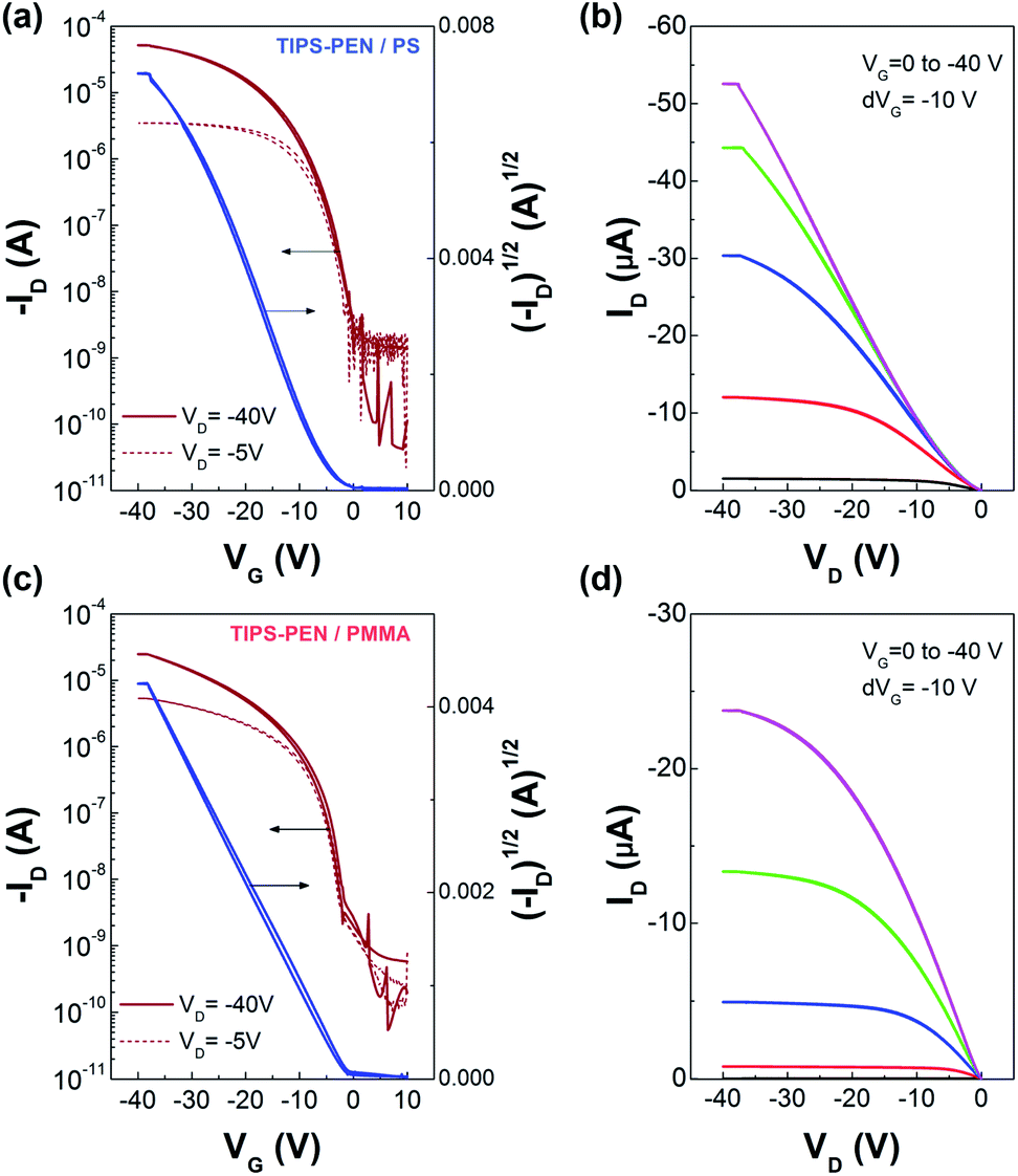
Fig. 8, shows the transfer and output characteristics of the PS- and PMMA-modified OFETs. All the I–V curves demonstrated unipolar p-type characteristics with distinct turn-on behaviour and good saturation properties both in the linear and saturation regime. The deviation from linearity at low VD in the output plots of the PS-modified OFETs, indicates the presence of a Schottky-like barrier which is attributed to non-ideality factors between the contacts and the semiconductor.38,39 Hardly any current hysteresis was observed in the I–V plots, confirming that the polar SiO2 surface was effectively passivated by the polymeric interlayers. The extracted electrical parameters are summarized and compared in Table 1. The PS- and PMMA-modified TIPS-PEN OFETs demonstrated field-effect mobilities up to 0.63 cm2 V−1 s−1 and 0.20 cm2 V−1 s−1 respectively, whereas the on/off current ratio in both cases was higher than 104. The considerable difference observed in the measured performance between the two alternate OFET types, is attributed to the different interfacial properties between the semiconductor and the assisting polymer. Specifically, the induced local morphological changes in the TIPS-PEN/PMMA interface as shown above, may cause disruption of the π–π stacking interaction. On the other hand, TIPS-PEN/PS samples maintained a better molecular interface which leads to a significant increase of the charge carrier mobility. It is worth mentioning that both OFETs consistently exhibited near zero threshold voltages, implying the low charge traps density in the accumulation channel.
 | ||
| Fig. 8 Transfer and output characteristics of the self-aligned TIPS-PEN OFETs with polymeric modifying layers of PS (a and b), PMMA (c and d). Devices had a top-contact/bottom-gate architecture and were measured at VD = −5 V (linear) and VD = −40 V (saturation). | ||
| Samples | μ avg (cm2 V−1 s−1) | μ max (cm2 V−1 s−1) | V T (V) | I on/Ioff | SS (V dec−1) |
|---|---|---|---|---|---|
| TIPS-PEN/PVP/glass | 0.58 | 0.72 | −2.6 (±1.7) | 1.2 × 10⁴ | 1.82 |
| TIPS-PEN/PS/SiO2/Si | 0.52 | 0.63 | −3.5 (±1.1) | 4.8 × 10⁵ | 2.18 |
| TIPS-PEN/PMMA/SiO2/Si | 0.15 | 0.20 | −1.9 (±1.4) | 1.1 × 10⁵ | 1.96 |
Charge carrier mobility is undoubtedly one of the most important parameters for the evaluation of OFETs performance. However, other characteristics like the operational and environmental stability are also considered essential in order to obtain a better image of the transistors functionality. Accordingly, stress measurements were carried out at a fixed gate bias of −40 V for various timings up to 104 s, at room temperature and ambient conditions and the effects on the drain current and threshold voltage were monitored. Fig. 9a and b, shows the evolution of transfer characteristics in the saturation regime (VG = VD = −40 V), as a function of stress time. The observed shift towards the negative direction, indicates an alteration of the threshold voltage, defined as ΔVT. Simultaneously, a decay in the source–drain current is also apparent and more pronounced in higher stress times. Notably, after the first 103 s only a slight decrease of approximately 13% in the drain current and a threshold voltage shift of less than −5 V were observed for both types of devices. Additionally, only marginal differences were seen in the slopes and the hysteresis of the transfer characteristics. The VT fluctuations are mostly ascribed to the charge trapping which takes place in the dielectric/semiconductor interface. The threshold voltage instability can be described by the following stretched-exponential function:40
 | (2) |
 | (3) |
 | ||
Fig. 9 Evolution of the transfer curves of the (a) PS and (b) PMMA-modified OFETs with increasing time (0–104 s), under a gate bias of −40 V. Panels (c and d) show the threshold voltage shift (ΔVT) and the plot of ΔVT/ΔVovs. time. Transfer characteristics measured in blade-coated TIPS-PEN OFETs modified using (e) PS or (f) PMMA before and after 3 months exposure. Insets show the  plots. plots. | ||
The environmental stability of the devices was investigated by exposing a batch of fabricated transistors for a long period (∼3 months) in normal ambient conditions. Fig. 9e and f, shows a comparison in the transfer characteristics between the freshly-prepared and the air-exposed transistors. Both devices exhibited a negligible positive shift in the threshold voltage as well as a slight increase in the hysteresis between forward and backward scans. Moreover, a slight decrease was also observed in the on-current and the on/off current ratio. These results further confirm the long term environmental stability of the devices arising from their effective passivation by the polymeric interlayers.
4. Conclusions
In summary, we have successfully designed a novel and facile method (“non-isotropic solvent evaporation”) which induces control over the crystalline orientation and the growth direction of TIPS-PEN blade-coated films. The versatility of the proposed experimental setup was evaluated by fabricating OFETs on two alternate substrates. Specifically, the OFETs incorporating crosslinked-PVP dielectric on glass substrates yielded high mobility values up to 0.72 cm2 V−1 s−1, as a consequence of the enhanced crystal orientation and the preferential molecular stacking. In the case of OFETs on conventional Si/SiO2 substrates, hydroxyl-free polymeric (PS or PMMA) assisting layers were incorporated in order to accommodate the appropriate wetting characteristics between the active solution and the hydrophilic SiO2 surface. The electrical characteristics of these devices revealed a reliable performance with negligible hysteresis, low threshold voltage and promising mobility values, up to 0.63 cm2 V−1 s−1 and 0.20 cm2 V−1 s−1 for the PS- and PMMA-modified OFETs, respectively. The evident difference in the measured performance between the two modified devices can be attributed to the interfacial phenomena, occurring during TIPS-PEN/polymer interaction. Furthermore, the utilization of polymeric interlayers onto the SiO2/Si substrates resulted in great operational and environmental stability as a consequence of the high crystalline quality and the subsequent efficient passivation. The presented experimental aspects open interesting perspectives towards the control over the crystalline morphology and encourage further studies on other solution-processed crystalline materials.Acknowledgements
This work was partially supported by: (a) European Union (European Social Fund – ESF) and Greek national funds through the Operational Program “Education and Lifelong Learning” of the National Strategic Reference Framework (NSRF) - Research Funding Program: Heracleitus II and (b) EC Project REGPOT-286022 ROleMak.References
- J. A. Rogers, Z. Bao, K. Baldwin, A. Dodabalapur, B. Crone, V. R. Raju, V. Kuck, H. Katz, K. Amundson, J. Ewing and P. Drzaic, Proc. Natl. Acad. Sci. U. S. A., 2001, 98, 4835–4840 CrossRef CAS PubMed.
- C. D. Sheraw, L. Zhou, J. R. Huang, D. J. Gundlach, T. N. Jackson, M. G. Kane, I. G. Hill, M. S. Hammond, J. Campi, B. K. Greening, J. Francl and J. West, Appl. Phys. Lett., 2002, 80, 1088 CrossRef CAS PubMed.
- G. H. Gelinck, H. E. A Huitema, E. van Veenendaal, E. Cantatore, L. Schrijnemakers, J. B. P. H. van der Putten, T. C. T. Geuns, M. Beenhakkers, J. B. Giesbers, B.-H. Huisman, E. J. Meijer, E. M. Benito, F. J. Touwslager, A. W. Marsman, B. J. E. van Rens and D. M. de Leeuw, Nat. Mater., 2004, 3, 106–110 CrossRef CAS PubMed.
- T. W. Kelley, P. F. Baude, C. Gerlach, D. E. Ender, D. Muyres, M. A. Haase, D. E. Vogel and S. D. Theiss, Chem. Mater., 2004, 16, 4413–4422 CrossRef CAS.
- K. Myny, S. Steudel, S. Smout, P. Vicca, F. Furthner, B. van der Putten, A. K. Tripathi, G. H. Gelinck, J. Genoe and W. Dehaene, Org. Electron., 2010, 11, 1176–1179 CrossRef CAS PubMed.
- T. Someya, Y. Kato, T. Sekitani, S. Iba, Y. Noguchi, Y. Murase, H. Kawaguchi and T. Sakurai, Proc. Natl. Acad. Sci. U. S. A., 2005, 102, 12321–12325 CrossRef CAS PubMed.
- D. A. Bernards, D. J. Macaya, M. Nikolou, J. A. DeFranco, S. Takamatsu and G. G. Malliaras, J. Mater. Chem., 2008, 18, 116–120 RSC.
- T. Sekitani, T. Yokota, U. Zschieschang, H. Klauk, S. Bauer, K. Takeuchi, M. Takamiya, T. Sakurai and T. Someya, Science, 2009, 326, 1516–1519 CrossRef CAS PubMed.
- Y. Ito, A. a. Virkar, S. Mannsfeld, J. H. Oh, M. Toney, J. Locklin and Z. Bao, J. Am. Chem. Soc., 2009, 131, 9396–9404 CrossRef CAS PubMed.
- J. E. Anthony, J. S. Brooks, D. L. Eaton and S. R. Parkin, J. Am. Chem. Soc., 2001, 123, 9482–9483 CrossRef CAS.
- J. E. Anthony, D. L. Eaton and S. R. Parkin, Org. Lett., 2002, 4, 15–18 CrossRef CAS PubMed.
- Y. Diao, B. C.-K. Tee, G. Giri, J. Xu, D. H. Kim, H. A. Becerril, R. M. Stoltenberg, T. H. Lee, G. Xue, S. C. B. Mannsfeld and Z. Bao, Nat. Mater., 2013, 12, 665–671 CrossRef CAS PubMed.
- R. L. Headrick, S. Wo, F. Sansoz and J. E. Anthony, Appl. Phys. Lett., 2008, 92, 063302 CrossRef PubMed.
- J. Chen, C. K. Tee, M. Shtein, D. C. Martin and J. Anthony, Org. Electron., 2009, 10, 696–703 CrossRef CAS PubMed.
- C. S. Kim, S. Lee, E. D. Gomez, J. E. Anthony and Y.-L. Loo, Appl. Phys. Lett., 2008, 93, 103302 CrossRef PubMed.
- S. K. Park, D. A. Mourey, J.-I. Han, J. E. Anthony and T. N. Jackson, Org. Electron., 2009, 10, 486–490 CrossRef CAS PubMed.
- S. K. Park, T. N. Jackson, J. E. Anthony and D. A. Mourey, Appl. Phys. Lett., 2007, 91, 063514 CrossRef PubMed.
- D. Choi, B. Ahn, S. H. Kim, K. Hong, M. Ree and C. E. Park, ACS Appl. Mater. Interfaces, 2012, 4, 117–122 CAS.
- Y. Su, X. Gao, J. Liu, R. Xing and Y. Han, Phys. Chem. Chem. Phys., 2013, 15, 14396–14404 RSC.
- G. Giri, E. Verploegen, S. C. B. Mannsfeld, S. Atahan-Evrenk, D. H. Kim, S. Y. Lee, H. A Becerril, A. Aspuru-Guzik, M. F. Toney and Z. Bao, Nature, 2011, 480, 504–508 CrossRef CAS PubMed.
- J. Jang, S. Nam, K. Im, J. Hur, S. N. Cha, J. J. M. Kim, H. Bin Son, H. Suh, M. A. Loth, J. E. Anthony, J.-J. J. Park, C. E. Park and K. Kim, Adv. Funct. Mater., 2012, 22, 1005–1014 CrossRef CAS.
- M. J. Kim, H. W. Heo, Y. K. Suh and C. K. Song, Org. Electron., 2011, 12, 1170–1176 CrossRef CAS PubMed.
- W. H. Lee, D. H. Kim, Y. Jang, J. H. Cho, M. Hwang, Y. D. Park, Y. H. Kim, J. I. Han and K. Cho, Appl. Phys. Lett., 2007, 90, 132106 CrossRef PubMed.
- Z. He, J. Chen, Z. Sun, G. Szulczewski and D. Li, Org. Electron., 2012, 13, 1819–1826 CrossRef CAS PubMed.
- C.-Y. Chen, H.-W. Chang, Y.-F. Chang, B.-J. Chang, Y.-S. Lin, P.-S. Jian, H.-C. Yeh, H.-T. Chien, E.-C. Chen, Y.-C. Chao, H.-F. Meng, H.-W. Zan, H.-W. Lin, S.-F. Horng, Y.-J. Cheng, F.-W. Yen, I.-F. Lin, H.-Y. Yang, K.-J. Huang and M.-R. Tseng, J. Appl. Phys., 2011, 110, 094501 CrossRef PubMed.
- B. Park and M. Han, Opt. Express, 2009, 17, 21362–21369 CrossRef CAS PubMed.
- M. M. Payne, S. R. Parkin, J. E. Anthony, C. Kuo and T. N. Jackson, J. Am. Chem. Soc., 2005, 127, 4986–4987 CrossRef CAS PubMed.
- Y. Jang, J. Jo and D.-S. Kim, J. Polym. Sci., Part B: Polym. Phys., 2011, 49, 1590–1596 CrossRef CAS.
- B. Park, H. G. Jeon, J. Choi, Y. K. Kim, J. Lim, J. Jung, S. Y. Cho and C. Lee, J. Mater. Chem., 2012, 22, 5641 RSC.
- J. Lim, W. Lee, D. Kwak and K. Cho, Langmuir, 2009, 25, 5404–5410 CrossRef CAS PubMed.
- J. Chen, C. K. Tee, J. Yang, C. Shaw, M. Shtein, D. C. Martin and J. Anthony, J. Polym. Sci., Part B: Polym. Phys., 2008, 46, 1878–1878 CrossRef CAS.
- D. Prime, S. Paul and P. Josephs-Franks, IEEE Trans. Dielectr. Electr. Insul., 2008, 15, 905–909 CrossRef CAS.
- J. Veres, S. Ogier, G. Lloyd and D. de Leeuw, Chem. Mater., 2004, 16, 4543–4555 CrossRef CAS.
- M.-B. Madec, D. Crouch, G. R. Llorente, T. J. Whittle, M. Geoghegan and S. G. Yeates, J. Mater. Chem., 2008, 18, 3230 RSC.
- J. Smith, R. Hamilton, I. McCulloch, N. Stingelin-Stutzmann, M. Heeney, D. D. C. Bradley and T. D. Anthopoulos, J. Mater. Chem., 2010, 20, 2562 RSC.
- M.-H. Yoon, C. Kim, A. Facchetti and T. J. Marks, J. Am. Chem. Soc., 2006, 128, 12851–12869 CrossRef CAS PubMed.
- M. Y. J. Cho, Y. D. Han, H. S. Kang, K. K. H. Kim, D. H. Choi and J. Joo, J. Appl. Phys., 2010, 107, 033711 CrossRef PubMed.
- D. Gupta, N. Jeon and S. Yoo, Org. Electron., 2008, 9, 1026–1031 CrossRef CAS PubMed.
- D. Boudinet, M. Benwadih, S. Altazin, R. Gwoziecki, J. M. Verilhac, R. Coppard, G. Le Blevennec, I. Chartier and G. Horowitz, Org. Electron., 2010, 11, 291–298 CrossRef CAS PubMed.
- F. R. Libsch and J. Kanicki, Appl. Phys. Lett., 1993, 62, 1286 CrossRef PubMed.
- H. H. Choi, W. H. Lee and K. Cho, Adv. Funct. Mater., 2012, 22, 4833–4839 CrossRef CAS.
- S. G. J. Mathijssen, M. Kemerink, a. Sharma, M. Cölle, P. A. Bobbert, R. A. J. Janssen and D. M. deLeeuw, Adv. Mater., 2008, 20, 975–979 CrossRef CAS.
- C. Liu, Y. Xu, Y. Li, W. Scheideler and T. Minari, J. Phys. Chem. C, 2013, 117, 12337–12345 CAS.
- X.-H. Zhang, S. P. Tiwari and B. Kippelen, Org. Electron., 2009, 10, 1133–1140 CrossRef CAS PubMed.
- J. H. Park, Y. T. Lee, H. S. Lee, J. Y. Lee, K. Lee, G. B. Lee, J. Han, T. W. Kim and S. Im, ACS Appl. Mater. Interfaces, 2013, 5, 1625–1629 CAS.
- K. P. Pernstich, S. Haas, D. Oberhoff, C. Goldmann, D. J. Gundlach, B. Batlogg, A. N. Rashid and G. Schitter, J. Appl. Phys., 2004, 96, 6431 CrossRef CAS PubMed.
| This journal is © The Royal Society of Chemistry 2014 |