The impact of selective solvents on the evolution of structure and function in solvent annealed organic photovoltaics†
Sheng
Hu
ab,
Ondrej
Dyck
bc,
Huipeng
Chen
bd,
Yu-che
Hsiao
bc,
Bin
Hu
bc,
Gerd
Duscher
bc,
Mark
Dadmun
bd and
Bamin
Khomami
*ab
aUniversity of Tennessee, Knoxville, Department of Chemical and Biomolecular Engineering, USA. E-mail: bkhomami@utk.edu
bSustainable Energy Education and Research Center, (SEERC), USA
cUniversity of Tennessee, Knoxville, Department of Materials Science and Engineering, USA
dUniversity of Tennessee, Knoxville, Department of Chemistry, USA
First published on 4th June 2014
Abstract
This study examines the development of structure and performance in an organic photovoltaic (OPV) thin film comprised of poly(3-hexylthiophene) (P3HT) and [6,6]-phenyl C61-butyric acid methyl ester (PCBM). Specifically, the influence of P3HT and PCBM solubility in the solvents utilized for vapor annealing on the morphological properties and OPV performance of the resultant active layer is examined. The evolution of P3HT crystallinity as well as the growth of PCBM aggregates in the solvent annealed thin films were examined by Grazing Incidence Wide Angle X-ray Scattering (GIWAXS), Atomic Force Microscopy (AFM), and Energy Filtered Transmission Electron Microscopy (EFTEM). It is shown that P3HT crystallinity increases initially, then decreases with time for solvents that have a finite P3HT solubility. Alternatively, PCBM aggregates grow continuously with SVA, but are modulated by the PCBM solubility. High P3HT crystallinity and moderate PCBM phase separation correlates to improved power conversion efficiency (PCE). Hence, the relative P3HT and PCBM solubility plays a crucial role in choosing the best SVA time of different annealing solvents. Specifically, for samples annealed using solvents that prefer P3HT, PCE benefits from further SVA after the peak P3HT crystallinity time, which is ascribed to additional PCBM phase separation. On the other hand, solvents that prefer PCBM induce excess PCBM phase separation at longer SVA times, which limits exciton dissociation and PCE. EFTEM cross section images indicate that PCBM is distributed toward the bottom of the film, whereas SVA in a solvent with high PCBM solubility may induce PCBM to segregate towards the air surface, which benefits charge transport processes by preventing electron–hole recombination.
1 Introduction
Organic photovoltaic (OPV) solar cells are a promising technology to provide clean and renewable energy, primarily because they are lightweight, low cost, and flexible.1–3 The archetypal bulk heterojunction (BHJ) cell consists of a mixture of regio-regular poly(3-hexylthiophene) (P3HT) and [6,6]-phenyl C61-butyric acid methyl ester (PCBM), which serve as electron donor and acceptor respectively.4–6 The power conversion efficiency (PCE) of this type of solar cell, i.e., the required exciton dissociation and charge transport, is a very intricate function of the morphology of the active layer.7,8In BHJ solar cells, excitons dissociate at the interface between the donor and the acceptor. In turn, the holes and electrons must travel to each electrode respectively.9 Thus, the ideal morphology of the BHJ active layer has often been depicted as a nanoscale phase separated structure with domains that are less than the exciton diffusion length (around 10–20 nm), including bi-continuous percolation paths for charge transport.10–13 Recently, a 3-phase model for the BHJ domain has also been proposed, namely, a system that contains a P3HT crystalline phase, a PCBM rich phase and a miscible amorphous phase of P3HT and PCBM, where the miscibility and interdiffusion of P3HT and PCBM plays a pivotal role in determining the nanoscale morphology.14,15 However, in most common fabrication processes, such as spin casting, solvent evaporation occurs very quickly, which kinetically blocks the evolution of the incipient structure, resulting in minimal crystallization and phase separation of the two components and a commensurate poor photovoltaic performance. In addition, it has been found that the electron acceptor material PCBM forms a PCBM-rich layer in the bottom of the thin film, which is attached to the PEDOT:PSS layer as well as the anode ITO glass in a conventional solar cell; while a P3HT-rich layer, which serves as the electron donor, prefers to occupy the top of the thin film, adjacent to the cathode. This vertical structure is created due to the different component surface energies γ (γ = 26.9 mN m−2 for P3HT and γ = 37.8 mN m−2 for PCBM)16 will result in a longer path-length for both transport of electrons and holes to each electrode, which in turn dramatically increase the probability of exciton recombination.17 As a result, a number of groups have adopted thermal annealing (TA) of the sample immediately after spin coating to allow the system to evolve towards equilibrium. Although thermal annealing induces in-plane π–π stacking of P3HT chains allowing easier charge transport from one grain to another, and improves the photovoltaic performance,18–20 the undesirable vertical structure can only be slightly modified. Moreover, the conjugated polymer may also suffer degradation or large-scale phase separation during TA at elevated temperatures, leading to poor photovoltaic cell performance.21 To this end, solvent vapor annealing (SVA) has been explored as an alternative method to impart molecule mobility of the BHJ components as well as P3HT crystallinity.8,22,23
During SVA, the OPV thin films are exposed to a specific solvent vapor environment, where the solvent molecules diffuse into the deposited layer, altering the nanoscale morphology. The thermodynamic driving forces that lead to these morphological changes are still not well understood. Several parameters such as treatment time, solubility of both polymer and fullerene in the solvent, and solvent vapor pressure, can dramatically impact the structural changes that occur during solvent annealing.24 However, it has been reported that solvents with high P3HT solubility can induce excess phase separation creating domains that exceed the exciton diffusion length so as to limit exciton dissociation.25,26 Meanwhile, the solubility of the fullerene derivatives also bear an impact on both P3HT and PCBM phase evolution.27,28 Hence, it is reasonable to expect that by adjusting the component solubility in the annealing solvent, the distribution of P3HT and PCBM phase can be tuned, thereby substantially reducing the exciton recombination rate. Thus, there is a critical need to fundamentally understand how these factors can be readily manipulated to impact the morphological evolution and optimize the solvent annealing process of BHJs.
To this end, a comprehensive experimental study has been conducted to ascertain the effect of SVA on the morphology and OPV performance of P3HT:PCBM active layers, using a series of organic solvents with different component solubility. The solubility of P3HT or PCBM in the examined solvents is measured by UV-vis. The crystalline structure and the phase separation behavior of the BHJ are first examined using Grazing Incidence Wide Angle X-ray Scattering (GIWAXS) and Atomic Force Microscopy (AFM). The power conversion efficiency of the resultant active layers are then measured to correlate the structure of the resultant P3HT:PCBM film and OPV function. In addition, Energy Filtered Transmission Electron Microscopy (EFTEM) has been utilized to examine the extent of both horizontal and vertical phase separation.
2 Experimental
2.1 Materials
All solvents were purchased from Aldrich and used as received. Regioregular P3HT (Mn = 37k, PDI-2.0, RR = 90–93%) and PC61BM (99.5%) were purchased from Reike Metals Inc., and Nano-C Inc., respectively.Silicon wafers were used as substrates and were first cleaned in hot piranha (1![[thin space (1/6-em)]](https://www.rsc.org/images/entities/char_2009.gif) :3 H2SO4:H2O2) for 30 min followed by washing in abundant deionized (DI) water and dried using a stream of nitrogen gas. P3HT:PCBM (1:0.8, w/w) was then dissolved in o-dichlorobenzene (ODCB) to achieve a solution with P3HT and PCBM concentrations of 10 mg ml−1 and 8 mg ml−1, respectively. By spin coating the solution on the silicon wafers, thin films with thickness of approximately 70 nm were obtained.
:3 H2SO4:H2O2) for 30 min followed by washing in abundant deionized (DI) water and dried using a stream of nitrogen gas. P3HT:PCBM (1:0.8, w/w) was then dissolved in o-dichlorobenzene (ODCB) to achieve a solution with P3HT and PCBM concentrations of 10 mg ml−1 and 8 mg ml−1, respectively. By spin coating the solution on the silicon wafers, thin films with thickness of approximately 70 nm were obtained.
2.2 Solvent annealing
Four solvents with different P3HT and PCBM solubilities and vapor pressures were used as the solvent in the solvent annealing process: bromobenzene (BB), chlorobenzene (CB), toluene (TL), 2-chlorophenol (2-CP). A detailed description of the experimental setup as well as the solubility measurement and surface vapor pressure calculation may be found in the ESI.†2.3 Characterization
 | (1) |
:PSS/P3HT:PC61BM (1:0.8, 9 mg ml−1)/Ca/Al were examined. PEDOT:PSS (40 nm, Baytron P 4083) was spin cast on top of pre-cleaned and UV-treated ITO substrates, then baked at 125 °C for 15 min. The active layer was spin cast on top of PEDOT:PSS in a glove box at 1000 rpm for 90 s. Thereafter, solvent annealing was carried out as described in the ESI.† The device preparation was followed by thermal deposition of 40 nm Ca and 80 nm Al under a vacuum of 3 × 10⁻⁷ Torr. All the devices were encapsulated before characterization and the non-annealed devices were used as control devices. The photovoltaic parameters were deduced from current density versus voltage (I–V) characterization by using a Keithley 2400 source meter under photo-illumination of AM 1.5G 100 mW cm−2 from a Thermal Oriel 96000 300 W solar simulator.
Sample preparation for plan view samples was performed using a float-off technique whereby the P3HT:PCBM layer was removed from a silicon substrate by immersion in deionized water. The water was then drained so that the P3HT:PCBM film came to rest on a 400 mesh copper TEM grid. Each sample was dried in a slide warmer at 60 °C overnight.
Energy filtered TEM (EFTEM) images have been used with success to determine phase separation in similar heterojunction samples.30–32 Following the established techniques, images were taken with a slit width of 8 eV centered at 19 and 30 eV. The resulting images are artificially colored blue and yellow, and superimposed. In these composite images a distinct phase separation between the P3HT and PCBM can readily be seen. This allows qualitative analysis of structure sizes and interconnectivity.
3 Results and discussion
3.1 Grazing Incidence Wide Angle X-ray Sacttering (GIWAXS)
The GIWAXS curves of the P3HT/PCBM spin-coated film illustrates a distinctive (100) crystalline peak of P3HT at 2θ = 5.4°. The area under the (100) peak and the full width at half maximum (FWHM) of the peak represents the P3HT crystallinity and crystal size (L) respectively.Fig. 1 shows the change in the area of the (100) P3HT peak with solvent annealing time for the solvents studied. All samples exhibit an increase in crystallinity after initial exposure to each solvent vapor. This is attributed to an enhanced P3HT mobility imparted by the presence of solvent vapor, which allows P3HT to crystallize. However, for the three solvents with P3HT solubility ∼>1 mg ml−1, i.e., BB, CB, and TL, the crystallinity decreases dramatically when exposure to solvent vapor exceeds a critical time. This loss of crystallinity is attributed to the dissolution of the P3HT crystals by the absorbed solvent vapor which, according to our previous research work,33 evaporates instantly after being taken out of the SVA column, leaving no time for the dissolved P3HT to re-crystallize. Besides, the color of the thin films change from dark purple to dark gray after SVA over one hour, indicating some permanent defects in P3HT structures might be generated that further prevent it from re-crystallization upon drying. However, the crystallinity of P3HT in the sample that was vapor annealed in 2-CP does not show this decrease, as 2-CP is a non-solvent for P3HT. Clearly polymer solubility plays a critical role in ordering of the polymer chains during solvent annealing. However, it should also be noted that the P3HT crystallinity increases at early solvent annealing times in 2-CP. This increase in crystallinity at the onset of SVA in 2-CP is ascribed to the high solubility of PCBM in 2-CP and miscibility of PCBM in amorphous P3HT.14,15,34,35 For all the SVA samples in this study, the time at which the maximum crystallinity is reached is inversely proportional to the P3HT solubility. Clearly, higher P3HT solubility increases the amount and rate of absorbed solvent vapor; thus, allowing the P3HT chains to more readily assemble into the crystalline form.
 | ||
| Fig. 1 Area of the P3HT (100) peak in the various solvent annealed P3HT/PCBM samples: (a) BB; (b) CB; (c) TL; (d) 2-CP. | ||
Fig. 2 shows the evolution of P3HT crystal size in each solvent annealed thin film as calculated from the FWHM of (100) peaks. Unlike P3HT crystallinity evolution, the P3HT crystal sizes decrease continuously for the samples that are solvent annealed in solvents with finite P3HT solubility. This is because in the initial stages of SVA, the absorbed solvent vapor induces amorphous P3HT to crystallize first via enhancing molecule mobility of P3HT, thereby increasing the overall crystallinity. However, these newly formed crystals are relatively small in size, therefore the average P3HT crystal size is reduced in this stage. As SVA proceeds, absorbed solvent vapor starts to dissolve already formed crystals, which results in a diminished degree of crystallinity as well as smaller crystal size. However, in the case of 2-CP annealing, the crystal size remains relatively constant which demonstrates the dissolution and formation of the P3HT crystals during SVA is mainly influenced by the P3HT solubility in the annealing solvent. Further experimental results on the evolution of the crystallinity in pure P3HT films during SVA confirm these results and can be found in the ESI† Section.
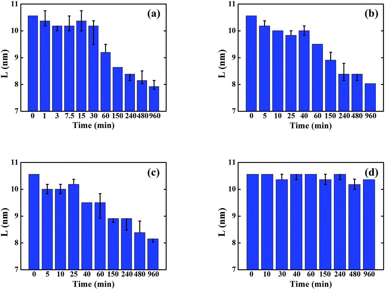 | ||
| Fig. 2 P3HT crystal sizes of the P3HT/PCBM sample annealed in various solvents: (a) BB; (b) CB; (c) TL; (d) 2-CP. | ||
3.2 Solar cell performance
To correlate the morphology changes that occur with SVA to the photovoltaic performance of the OPV active layer, nine identical solar cells were fabricated and solvent vapor annealed for the SVA conditions at time 1, corresponding to the P3HT crystallinity peak time and time 2, which is approximately double the peak time. The motivation behind choosing these two times is that the crystallinity of each sample at time 2 is only slightly lower than the peak time crystallinity. Therefore, PCBM phase separation becomes the primary factor that determines the performance of the active layer.The J–V curves and the corresponding PCE data for these samples are presented in Fig. 3 and Table 1. The as cast (AC) devices show a short-circuit current (Jsc) of 2.48 mA cm−2, an open-circuit voltage (Voc) of 0.59 V and a fill factor of 0.446, contributing to a poor PCE of 0.65%. The low values of Jsc and Voc comparing with other works are due to the relative small thickness of our sample. After SVA, the Jsc improves substantially for all solvent annealed samples, as a consequence of enhanced P3HT crystallinity and PCBM aggregation that benefits light absorption. The fill factor (FF), which corresponds to charge transfer mobility, also increases for most of the cases studied. On the other hand, a slight decrease of Voc is found for all devices after the annealing process, as ascribed to the reduced series resistance and charge transfer energy resulting from delocalized crystalline phase. To be more specific, at time 1, where all samples have attained peak P3HT crystallinity, the sample that is annealed in 2-CP exhibits the highest Jsc and FF, leading to an excellent PCE of 2.1%. The better improved cell performance is primarily a result of the moderate PCBM aggregation that benefits the charge transport process. At time 2, the samples annealed in BB and CB, which have relatively higher P3HT solubility than PCBM solubility show an increase in their Jsc, FF hence PCE, while a slight decrease of cell performance at time 2 is found for the other two samples, i.e., those annealed in TL and 2-CP which prefer PCBM over P3HT. This variation also possibly arises from the differences in the extent of PCBM phase segregation.
 | ||
| Fig. 3 J–V curves of solvent annealed P3HT/PCBM composite films. | ||
| Sample AC | Time (min) | (100) (peak area) | J sc (mA cm−2) | V oc (V) | FF | PCE | |
|---|---|---|---|---|---|---|---|
| 0 | 1420 | 2.482 | 0.591 | 44.6 | 0.65 | ||
| Time 1 | BB | 3 | 1909 | 4.183 | 0.587 | 42.4 | 1.04 |
| CB | 10 | 1931 | 5.974 | 0.567 | 44 | 1.49 | |
| TL | 40 | 1905 | 6.618 | 0.595 | 44.9 | 1.77 | |
| 2-CP | 30 | 1799 | 6.888 | 0.583 | 52.3 | 2.1 | |
| Time 2 | BB | 7.5 | 1621 | 6.832 | 0.543 | 45.8 | 1.7 |
| CB | 25 | 1882 | 6.486 | 0.567 | 54.3 | 2 | |
| TL | 60 | 1778 | 5.193 | 0.547 | 47.8 | 1.36 | |
| 2-CP | 60 | 1794 | 6.684 | 0.575 | 47.7 | 1.83 | |
Therefore, the development of PCBM phase separation during different solvent annealing processes was also investigated to account for the aforementioned changes in the performance of the samples. Here we utilized AFM and TEM respectively to study the SVA induced evolution of surface PCBM morphology as well as horizontal and vertical PCBM distribution within the sample.
3.3 AFM measurements
The comparison of the phase contrast images (Fig. S3†) first indicates that there is a continuous increase of PCBM aggregation as well as RMS roughness (Fig. S4a,† calculated from the 5 μm × 5 μm height images) at the surface of the P3HT/PCBM thin film during CB SVA. This could be attributed to PCBM phase separation that occurs with increased molecular mobility, while the high solvent concentration on the film surface could induce a more pronounced surface phase separation of PCBM. Further comparison of the surface morphologies of each solvent annealed sample at time 1 and 2 also shows that surface PCBM aggregation and RMS roughness is always higher at longer times (time 2), see Fig. 4 and S4b.† | ||
| Fig. 4 AFM image of solvent annealed thin film at time 1 (left two columns) and time 2 (right two columns). In each time, left column: 5 μm × 5 μm phase image; right column: 5 μm × 5 μm height image. | ||
3.4 TEM measurements
To further establish the relationship between PCBM phase separation and solar cell performance, EFTEM images for both horizontal and vertical P3HT/PCBM phase distribution were obtained for as cast sample as well as four typical samples with different PCBM aggregation and PCE performances, i.e., BB at time 1, CB at time 1, 2-CP at time 1 and TL at time 2 (see Fig. 5 and 6). The energy windows were positioned at 19 eV for P3HT and 30 eV for PCBM, marked as blue and yellow respectively. The dark and light areas are caused by thickness variations as verified in zero energy filtered images (not shown). The as cast sample barely shows any P3HT/PCBM phase separation, as demonstrated by both horizontal and vertical EFTEM images. The horizontal PCBM phase separation in Fig. 5 indicates that the TL time 2 sample has the largest PCBM domain size, corresponding to the highest PCBM phase separation, followed by the 2-CP, CB and BB annealed samples at their P3HT crystallization peak time. When we compare these results with their PCE, we can conclude that a moderate PCBM domain size, i.e., 2-CP time 1, produces the best OPV performance. | ||
| Fig. 5 EFTEM images showing the solvent chosen for solvent annealing has a clear effect on the promotion of phase separation between P3HT and PCBM. Blue corresponds to an energy window at 19 eV (P3HT), yellow corresponds to an energy window at 30 eV (PCBM). The dark and light areas are caused by thickness variations as verified in zero energy filtered images (not shown). | ||
 | ||
| Fig. 6 EFTEM images in cross-section reveal the vertical P3HT/PCBM phase distribution before and after vapor annealing with different solvents. The Si substrate appears blue due to the large bulk plasmon peak of Si near the 19 eV energy window. | ||
For the vertical PCBM distribution (Fig. 6), we also see a thin layer of textured material under the platinum cap. This is a result of the ion beam platinum deposition directly onto the polymer material during sample preparation. From Fig. 6 it is evident that PCBM is more prevalent in the bottom of the thin film (closest to the Si substrate), leaving the P3HT phase on top. The distribution of a P3HT-rich layer on top and a PCBM-rich layer on the bottom is in agreement with prior studies, and is primarily due to the difference between P3HT and PCBM surface energies, which induce selective molecule segregation during spin coating.16,17
When comparing vertical phase separation in Fig. 6, the BB time 1 sample shows little contrast between P3HT and PCBM, which means there is little vertical phase separation. The film annealed with CB at time 2 exhibits some vertical phase separation, however, more PCBM is found near the bottom layer, which is detrimental to the cell performance. The sample annealed with 2-CP at time 1 illustrates a more evenly distributed PCBM phase along the film thickness, which is due to the enhanced PCBM molecule mobility by the solvent. Although the TL time 2 sample (Fig. 4) also exhibits a well vertically distributed PCBM phase, nevertheless, excess PCBM aggregation reduces the P3HT/PCBM interface for exciton dissociation and charge transport, resulting in a decreased PCE when compared with the sample annealed in 2-CP at time 1.
Comparing with the AFM results, the PCBM domain sizes revealed through EFTEM show the same trends as their PCBM surface aggregations and RMS roughness, which demonstrates that the surface roughness may be correlated to the PCBM aggregation/phase separation throughout the film, and is driven by both PCBM solubility and SVA time. Also, the rate of P3HT crystal growth is governed by the solubility of P3HT in the annealing solvents, as indicated previously. Therefore, the relative solubility, i.e., the ratio of P3HT solubility to PCBM solubility, plays a critical role in defining the optimal SVA time for each solvent. Specifically, the samples that are vapor annealed in BB and CB have relatively small PCBM phase separation at the time of maximum P3HT crystallinity, which may be ascribed to the fact that P3HT is more soluble than PCBM in those two solvents. This preference for P3HT results in better enhanced P3HT molecular mobility, which brings about a faster P3HT crystallization than PCBM aggregation. In turn, this translates to insufficient time for PCBM aggregation, at the peak P3HT crystallinity time limiting electron transport. Further SVA enables more PCBM aggregation, providing more pathways for electron transport and benefiting cell performance.
On the other hand, PCBM has a higher solubility in TL and 2-CP than P3HT. This results in faster PCBM phase separation at the P3HT crystallinity peak time, which produces better cell performance for the TL and 2-CP annealed samples at their peak times. Excessive PCBM aggregation is induced at longer annealing times for these two samples, which reduces P3HT/PCBM interfacial area and exciton dissociation, as well as introducing the potential for the formation of isolated PCBM domains, which also limits charge transport. Therefore, a reduced PCE is found in these samples.
4 Conclusion
The solubility of P3HT and PCBM in the annealing solvent clearly impacts the development of the morphology of P3HT/PCBM active layers during solvent vapor annealing, which in turn determines the OPV performance of the resultant solar cell. Two distinct phenomena are observed in the morphological progression of the solvent annealed thin films: an evolution of P3HT crystallinity as well as the development of PCBM phase separation. More importantly, these two structural features can be tuned separately.For the solvents that have a finite P3HT solubility, SVA initially increases P3HT crystallinity below a critical time. Solvent vapor annealing beyond this optimum time lowers crystallinity presumably by dissolving already formed P3HT crystals. The solubility of P3HT in the vapor annealing solvent is pivotal in determining the variation of P3HT crystallinity with solvent annealing. However, the P3HT/PCBM sample that is solvent annealed in 2-chlorophonel vapor, which has negligible P3HT solubility also favors P3HT crystallinity enhancement by aiding P3HT mobility in the miscible amorphous phase.
A PCBM-rich phase, formed by PCBM aggregation continuously grows with solvent vapor annealing for all solvents studied. The rate of this growth is controlled by the PCBM solubility in the annealing solvent. As might be expected, moderate PCBM aggregation, is preferred, as extended phase segregation reduces interfacial area between P3HT and PCBM, limiting exciton dissociation. Similarly, excess segregation can lead to isolated domains that limit charge transport to the electrodes; both factors will decrease PCE performance.
Just as the rate of P3HT crystal growth is controlled by the solubility of P3HT in the vapor annealing solvents, the PCBM solubility directs the PCBM aggregation, therefore relative P3HT/PCBM solubility is critical in defining the right SVA time. Active layers that are annealed in solvents that prefer P3HT (BB and CB in this study) form a P3HT pathway for charge transport before the formation of PCBM domains that are able to support efficient electron transport to the electrodes. These samples benefit from further solvent annealing to allow additional PCBM aggregation, but risk the loss of P3HT crystallinity.
P3HT/PCBM thin films that are solvent annealed in solvents that prefer PCBM (TL and 2-CP in this study) show a decrease in active layer performance with excess solvent annealing. This can be ascribed to phase segregation of the PCBM into larger and potentially inaccessible domains that limit exciton dissociation and charge transport pathways to the electrode.
Plane view EFTEM images and AFM surface analysis confirm the relationship between PCE and PCBM aggregation, indicating the best PCE corresponds to a moderate PCBM phase separation. Cross sectional P3HT/PCBM phase distribution illustrates an upward movement of PCBM molecules for the samples annealed by solvents that have higher PCBM solubility (2-CP and TL). This benefits the cell performance by providing a more direct path to each electrode.
Acknowledgements
The authors wish to acknowledge financial support from the National Science Foundation (CBET-0932666), as well as the support of the Sustainable Energy Education Research Center and TNSCORE at the University of Tennessee. We also thank Dr Joseph E. Spruiell for assistance with GIWAXS analysis.References
- F. C. Krebs, Sol. Energy Mater. Sol. Cells, 2009, 93, 394–412 CrossRef CAS PubMed
.
- L.-M. Chen, Z. Hong, G. Li and Y. Yang, Adv. Mater., 2009, 21, 1434–1449 CrossRef CAS
- J. Peet, M. L. Senatore, A. J. Heeger and G. C. Bazan, Adv. Mater., 2009, 21, 1521–1527 CrossRef CAS
- S. S. v. Bavel, E. Sourty, G. d. With and J. Loos, Nano Lett., 2009, 9, 507–513 CrossRef PubMed
- T. Savenije, J. Kroeze, X. Yang and J. Loos, Adv. Funct. Mater., 2005, 15, 1260–1266 CrossRef CAS
- W. Ma, C. Yang, X. Gong, K. Lee and A. Heeger, Adv. Funct. Mater., 2005, 15, 1617–1622 CrossRef CAS
- G. Dennler, M. C. Scharber and C. J. Brabec, Adv. Mater., 2009, 21, 1323–1338 CrossRef CAS
- G. Li, V. Shrotriya, J. Huang, Y. Yao, T. Moriarty, K. Emery and Y. Yang, Nat. Mater., 2005, 4, 864–868 CrossRef CAS
-
H. S. Nalwa, Handbook of Organic Conductive Molecules and Polymers, Wiley, 1997, vol. 3 Search PubMed
-
G. Yu, J. Gao, J. Hummelen, F. Wudl and A. Heeger, Science-AAAS-Weekly Paper Edition, 1995, vol. 270, pp. 1789–1790 Search PubMed
- J. Halls, C. Walsh, N. Greenham, E. Marseglia, R. Friend, S. Moratti and A. Holmes, Nature, 1995, 376, 498–500 CrossRef CAS
- A. Gadisa, W. Mammo, L. Andersson, S. Admassie, F. Zhang, M. Andersson and O. Inganäs, Adv. Funct. Mater., 2007, 17, 3836–3842 CrossRef CAS
- H.-Y. Chen, J. Hou, S. Zhang, Y. Liang, G. Yang, Y. Yang, L. Yu, Y. Wu and G. Li, Nat. Photonics, 2009, 3, 649–653 CrossRef CAS
- W. Yin and M. Dadmun, ACS Nano, 2011, 5, 4756–4768 CrossRef CAS PubMed
- H. Chen, R. Hegde, J. Browning and M. D. Dadmun, Phys. Chem. Chem. Phys., 2012, 14, 5635–5641 RSC
- D. S. Germack, C. K. Chan, R. J. Kline, D. A. Fischer, D. J. Gundlach, M. F. Toney, L. J. Richter and D. M. DeLongchamp, Macromolecules, 2010, 43, 3828–3836 CrossRef CAS
- H.-L. Yip and A. K.-Y. Jen, Energy Environ. Sci., 2012, 5, 5994 CAS
- M. T. Lloyd, J. E. Anthony and G. G. Malliaras, Mater. Today, 2007, 10, 34–41 CrossRef CAS
- H. Kim, W.-w. So and S.-j. Moon, J. Korean Phys. Soc., 2006, 48, 441–445 CAS
- S. Honda, T. Nogami, H. Ohkita, H. Benten and S. Ito, ACS Appl. Mater. Interfaces, 2009, 1, 804–810 CAS
- C. H. Woo, B. C. Thompson, B. J. Kim, M. F. Toney and J. M. J. Fréchet, J. Am. Chem. Soc., 2008, 130, 16324–16329 CrossRef CAS PubMed
- G. Li, Y. Yao, H. Yang, V. Shrotriya, G. Yang and Y. Yang, Adv. Funct. Mater., 2007, 17, 1636–1644 CrossRef CAS
- G. Lu, L. Li and X. Yang, Small, 2008, 4, 601–606 CrossRef CAS PubMed
- H. Tang, G. Lu, L. Li, J. Li, Y. Wang and X. Yang, J. Mater. Chem., 2010, 20, 683–688 RSC
- J.-H. Jou, P.-H. Chiang, Y.-P. Lin, C.-Y. Chang and C.-L. Lai, Appl. Phys. Lett., 2007, 91, 043504 CrossRef PubMed
- J. H. Park, J. S. Kim, J. H. Lee, W. H. Lee and K. Cho, J. Phys. Chem. C, 2009, 113, 17579–17584 CAS
- P. A. Troshin, H. Hoppe, J. Renz, M. Egginger, J. Y. Mayorova, A. E. Goryachev, A. S. Peregudov, R. N. Lyubovskaya, G. Gobsch, N. S. Sariciftci and V. F. Razumov, Adv. Funct. Mater., 2009, 19, 779–788 CrossRef CAS
- P. A. Troshin, D. K. Susarova, E. A. Khakina, A. A. Goryachev, O. V. Borshchev, S. A. Ponomarenko, V. F. Razumov and N. S. Sariciftci, J. Mater. Chem., 2012, 22, 18433–18441 RSC
-
S. R. S. B. D. Cullity, Elements of X-Ray Diffraction, Prentice Hall, 3rd edn, 2001 Search PubMed
- L. F. Drummy, R. J. Davis, D. L. Moore, M. Durstock, R. A. Vaia and J. W. P. Hsu, Chem. Mater., 2011, 23, 907–912 CrossRef CAS
- A. A. Herzing, L. J. Richter and I. M. Anderson, J. Phys. Chem. C, 2010, 114, 17501–17508 CAS
- M. Pfannmöller, H. Flügge, G. Benner, I. Wacker, C. Sommer, M. Hanselmann, S. Schmale, H. Schmidt, F. A. Hamprecht, T. Rabe, W. Kowalsky and R. R. Schröder, Nano Lett., 2011, 11, 3099–3107 CrossRef PubMed
- S. Hu, Masters thesis, University of Tennessee, 2013.
- N. D. Treat, M. A. Brady, G. Smith, M. F. Toney, E. J. Kramer, C. J. Hawker and M. L. Chabinyc, Adv. Energy Mater., 2011, 1, 82–89 CrossRef CAS
- D. Chen, A. Nakahara, D. Wei, D. Nordlund and T. P. Russell, Nano Lett., 2011, 11, 561–567 CrossRef CAS PubMed
Footnote |
| † Electronic supplementary information (ESI) available. See DOI: 10.1039/c4ra02257b |
| This journal is © The Royal Society of Chemistry 2014 |