Multilayer thin film encapsulation for organic light emitting diodes

Rakhi Grover*ab, Ritu Srivastava*a, M. N. Kamalasanana and D. S. Mehtab
aCenter for Organic Electronics, Physics of Energy Harvesting Division, CSIR-National Physical Laboratory, New Delhi 110012, India. E-mail: grover.rakhi@gmail.com; ritu@mail.nplindia.org
bDepartment of Physics, Indian Institute of Technology Delhi, New Delhi, India

Received 24th October 2013 , Accepted 23rd December 2013

First published on 2nd January 2014


Abstract

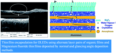
A transparent and effective thin film encapsulation (TFE) based on a multilayer structure is demonstrated. Alternate films of amorphous and crystalline film forming organic materials have been investigated to create complicated diffusion pathways for oxygen and water vapour, which was reflected in their increased barrier properties. These layers are further protected by an inorganic barrier coating of magnesium fluoride (MgF2) deposited by normal and glancing angle deposition methods. A significant enhancement of more than 8 times in the lifetime of organic light emitting diodes was obtained by employing this multilayer hybrid geometry. The TFE structure can be highly useful in organic opto-electronic devices requiring easy to deposit and an effective barrier layer for enhanced lifetimes.


1 Introduction

Organic opto-electronic devices are gaining large interest due to their potential use in flexible as well as large area display devices.1,2 The lifetime of organic semiconductor based devices is one of the most critical parameters in preserving the device performance for a longer time and therefore the major challenge for these devices.3,4 The most important and straightforward method to avoid degradation is to prevent these devices from degradation triggers, mainly oxygen and water. Since aluminium as a cathode alone, although thick, is not able to suppress the moisture and water ingress, the use of additional barrier layers to protect the device is indispensable. Thin film encapsulation is an attractive method to encapsulate flexible and large area opto-electronic devices due to its light weight, transparency and mechanical flexibility.5,6 In order to effectively protect the device, barrier films must have characteristics such as thermal stability, transparency, pin hole free coating and chemical resistance, as well as low moisture and oxygen permeation. Its deposition temperature should be low enough so that the underlying organic layers are not degraded. No single layer, whether organic or inorganic, can combine all these properties.

Several inorganic thin films have been reported to provide encapsulating barrier properties for organic semiconductor based devices.7,8 However, the processing temperature of the layers is too high for the direct application on top of devices composed of sensitive organic films. Furthermore, nano or micro sized defects or pin holes cannot be avoided.9 These defects usually originate from the deposition process itself or the roughness of the underlying layers. Apart from this, multiple inorganic layers are also not pertinent as these defects propagate throughout the layer during film growth itself. Therefore, alternating organic and inorganic thin layers are usually employed as barrier coatings for the purpose of decoupling such defects.10,11 The crystalline inorganic layers hinders water and oxygen ingress, whereas the amorphous organic layers tend to minimize pin holes by planarizing the inorganic barrier coating.12,13 However, such techniques involve the deposition of inorganic films alternatively within the hybrid TFE structure, which requires high temperature deposition as well as high cost vacuum equipments. Moreover, the technique requires different processing units and exposure of the devices to ambient atmosphere for encapsulation, thus complicating the procedure.

In contrast to these, organic materials have different morphological properties and can be used to produce the same environment. Such an alternating structure can then effectively decouple the defects present in a single layer and also requires the same vacuum chamber, thus simplifying the process.14 But, as the organic layers are themselves sensitive to the ambient atmosphere, the use of an effective inorganic layer cannot be avoided. Such an inorganic barrier coating can protect the organic–organic alternate geometry, thereby producing a simplified thin film encapsulation structure.

In addition, the properties of the inorganic layer can also be modified. Significant modifications in the physical properties of thin films are usually accomplished by varying the deposition parameters, such as the deposition rate, deposition angle, substrate temperature and pressure. Among these, glancing angle deposition (GLAD) is an attractive technique to generate a range of film morphologies just by varying the angle of the vapour flux incident on the substrate. Magnesium fluoride (MgF2) is known to be a hydrophobic as well as durable material resistant to mechanical and thermal stresses. It has also been investigated as a protective layer for flexible OLEDs. In addition, it can be uniformly deposited by vacuum thermal evaporation technique and is one of the strong column forming materials. Columnar structures of MgF2 can be easily obtained by changing the incident vapour flux angles from 0° to 85°.15–17 Furthermore, the films deposited by GLAD technique, having assemblies of parallel columns, exhibit surfaces with enhanced hydrophobic properties,18,19 which are desirable to provide sufficient barrier protection to organic semiconductor based devices.

The present work reports a multilayer structure composed of two organic materials belonging to the same family of organic compounds, yet exhibiting entirely different morphological properties. N,N′-Diphenyl-N,N′-bis-3-methylphenyl(1,1′-biphenyl) (TPD) is well known to have a very low glass transition temperature (Tg) imparting poor thermal stability to the material. Thin films of TPD are readily crystallized20 as soon as the thicker TPD films are deposited, which is remarkable since the material tends to form crystals that are expected to result in different permeation pathways along the grain boundaries. Another organic film from the same family as TPD with a spiro structure (2,7-bis[N,N-bis(4-methoxy-phenyl)amino]-9,9-spirobifluorene) (Meo-Spiro-TPD) exhibits a relatively high glass transition temperature, thus imparting very high thermal stability to the material. Thin films of MeO-Spiro-TPD are relatively dense and amorphous with a substantially reduced density of defects. These thin films act as planarization layers. These layers provide efficient decoupling of the defects leading to a considerably slower diffusion of water vapour and oxygen into the device. To avoid the direct contact of these sensitive films with ambient atmosphere MgF2 films are used. Therefore, these layers are further protected by barrier coatings of normal and GLAD deposited MgF2. A glancing angle of 85° was chosen for depositing MgF2 because significant morphological changes, resulting in columnar structures, are observed at such high angles of incident vapour flux w.r.t the substrate normal.21–23 The barrier properties of encapsulating films have been studied in detail using calcium optical tests and OLED lifetime studies.

2 Experimental procedures

2.1 Thin film characterization

For calcium optical tests plain glass plates were used as the starting substrates and cleaned sequentially using de ionized water, acetone, trichloroethylene and isopropyl alcohol for 20 minutes each using an ultrasonic bath and then dried in a vacuum oven. Thin films of Ca (calcium) were deposited with a thickness of 250 nm under a high vacuum (2 × 10⁻⁶ Torr). Then alternate films of MeO-Spiro-TPD and TPD were deposited with thicknesses of 50 nm and 100 nm, respectively. The structure was then coated with inorganic thin films of MgF2 deposited by normal and glancing angle deposition methods at a vapor flux or glancing angles of 0° and 85°, respectively. The thicknesses of these films were measured in situ by a quartz crystal thickness monitor.

The calcium coated thin films were tested using calcium degradation tests. The corresponding device structures are given below and also shown in Fig. 1:

(a) Glass–Ca (i.e., calcium structure A).

(b) Glass–Ca–MeO-Spiro-TPD (50 nm)–TPD (100 nm) (i.e. a Ca film encapsulated within a multilayer stack of organic films. The devices were labelled, according to the number of layer pairs of MeO-Spiro-TPD–TPD, as Ca structures B1, B2, B3 and B4 for one, two, three and four stacks, respectively). The total thickness of the organic films over Ca film increased to 150, 300, 450 and 600 nm for the structures B1, B2, B3 and B4, respectively.

(c1) Glass–Ca–MeO-Spiro-TPD–TPD (three stacks)–normal MgF2 (i.e. Ca structure B3 coated with a 250 nm thick film of MgF2 deposited by normal deposition method, further called the Ca structure C1). The total thickness of the encapsulating films over the Ca film was 700 nm for the structure C1.

(c2) Glass–Ca–MeO-Spiro-TPD–TPD (three stacks)–normal MgF2–GLAD MgF2 (i.e. Ca structure B3 coated with MgF2 films deposited by normal deposition (50 nm thick) and glancing angle deposition (200 nm thick) methods at a vapor flux or glancing angle of 0° and 85°, respectively, further called the Ca structure C2). The total thickness of the encapsulating films over the Ca film was 700 nm for the structure C2.


image file: c3ra46077k-f1.tif
Fig. 1 Schematic diagrams showing the Ca device structures (a) A (b) B1, B2, B3, B4 and (c) C1 and C2 fabricated for the Ca tests.

Morphological properties of the organic thin films were examined using Atomic force microscopy (AFM) (NT-MDT). Transmission spectra were taken using a high resolution UV-Vis spectrophotometer (Shimadzu 2401 PC) in the range of 200–800 nm.

2.2 OLED fabrication

OLEDs were fabricated with and without the encapsulation layers. 120 nm thick indium-tin oxide (ITO) coated glass plates (with a sheet resistance of 20 Ω per square) were used as starting substrates. These were first patterned and then cleaned using various solvents sequentially and dried under vacuum. 4,4′,4′′-Tris(3-methyl-phenylphenylamino)triphenylamine (m-MTDATA) and N,N′-di-1-naphthalenyl-N,N′-diphenyl-1,1′biphenyl-4,4′-diamine (α-NPD) were used as hole injection and hole transporting layers, respectively. A thin film of 5% (Ir(ppy)3) doped (CBP) was used as the emissive layer. Pristine and 20 wt% tetracyanoquinodimethane (TCNQ) mixed 4,7-diphenyl-1,10 phenanthroline (BPhen) films were used as electron transport and electron injection layers respectively. The size of the pixels formed was 4 mm × 4 mm. The devices were further coated with TFE structures in the same vacuum chamber.

OLED with the following device structures were fabricated:

Device A: reference device without encapsulation.

Device B3: device encapsulated with 3 layer pairs of (MeO-Spiro-TPD–TPD) further called OLED structure B3.

Device C1: device encapsulated with 3 layer pairs of (MeO-Spiro-TPD–TPD) further covered with a barrier coating of MgF2 (250 nm thick) deposited by normal deposition method further called OLED structure C1.

Device C2: device encapsulated with 3 layer pairs of (MeO-Spiro-TPD–TPD) further covered with a barrier coating of MgF2 film deposited by normal deposition (50 nm thick) and glancing angle deposition (200 nm thick) methods at a vapor flux or glancing angle of 0° and 85° respectively, further called OLED structure C2.

The current density–voltage–luminescence (JVL) characteristics have been measured with a luminance meter (LMT-1009) interfaced with a Keithley 2400 programmable current–voltage digital source meter. All the measurements were carried out at room temperature under ambient conditions.

3 Results and discussion

Figure 2 shows the schematic view of the spiro concept and the chemical structures of the organic materials used for encapsulation in this study. TPD N,N′-diphenyl-N,N′-bis-3-methyl phenyl[1,1′-bipheny]-4,4′-diamine is well known as a hole transporting material in OLEDs but it is readily crystallized because of its low glass transition temperature (Tg = 64 °C). The spiro concept for charge transporting or emissive material was introduced by Salbeck in 1996.24 The schematic view of this concept is shown in Fig. 2(b). Joining the two TPD molecules with a spiro centre enhances Tg due to the raised steric demand of the spiro based structure.24 The resulting spiro compound has a greater Tg (115 °C) than its parent compound TPD (64 °C). The alternate stack of such materials with completely different thin film forming abilities can be used to enhance the diffusion pathways of ambient oxygen and water molecules thereby enhancing the barrier performance compared to a single layer.14
image file: c3ra46077k-f2.tif
Fig. 2 (a) Molecular structure of TPD, (b) schematic view of the spiro concept and (c) molecular structure of MeO-Spiro-TPD.24

3.1 Microstructural studies using AFM and SEM image analysis

The surface morphology of MeO-Spiro-TPD thin films was examined using AFM image analysis. Fig. 3 shows the AFM image of 50 nm thick films of MeO-Spiro-TPD as deposited on glass substrates. Thin films of the material were found to be dense, amorphous and stable with very low increase in roughness values even after 960 hours of storage. In this case, quite smooth films of MeO-Spiro-TPD were preferred for direct deposition on the cathode. The corresponding average roughness values are presented in Table 1.
image file: c3ra46077k-f3.tif
Fig. 3 AFM images of 50 nm thick films of MeO-Spiro-TPD (a) after deposition (b) after 20 days and (c) after 40 days of storage.
Table 1 Average roughness values of a thin film of MeO-Spiro-TPD with time
S. no. Time Average roughness value (nm)
1 After deposition 1.26 ± 0.023
2 After 480 hours (20 days) 1.68 ± 0.062
3 After 960 hours (40 days) 2.56 ± 0.072


Further, to analyse the growth of inorganic thin films of MgF2, these were deposited onto glass substrates. Fig. 4(a) and (b) show the scanning electron microscope (SEM) images of MgF2 thin films deposited by normal and glancing angle deposition (GLAD) methods at 0° and 85°, respectively. The cross-sectional images clearly show the formation of a continuous film by normal deposition (Fig. 4(a)) and columnar structures by GLAD method (Fig. 4(b)). The enlarged insets of the figures show the contact angle images and the respective values given by the software measurements to be 57° and 84° for Fig. 4(a) and (b), respectively, for the sessile deionised water drops. The GLAD deposited MgF2 films used in the present study exhibited enhanced water repelling properties compared to normally deposited MgF2 films. Similar results have been reported in the literature for encapsulation using columnar structures exhibiting water repelling properties.25 Choi et al.7 have also studied the water contact angles for the thin film encapsulants, Al2O3 and SiO2 films. The contact angles for Al2O3 and SiO2 were reported to be 74° and 5°, respectively, and the films were placed in the multilayer stack accordingly. Fig. 5 shows the SEM image of GLAD MgF2 thin films deposited over the organic alternate layers of TPD and MeO-Spiro-TPD. The feasibility of deposition of inorganic thin films of GLAD MgF2 over the organic multilayer stack can be easily seen in the inset of Fig. 5, which shows an enlarged view of the structure.


image file: c3ra46077k-f4.tif
Fig. 4 Scanning electron microscope (SEM) images of MgF2 thin films deposited by normal and glancing angle deposition methods at (a) 0° and (b) 85° vapor flux angles.

image file: c3ra46077k-f5.tif
Fig. 5 SEM image of GLAD MgF2 thin film deposited over the organic alternate structure of TPD and MeO-Spiro-TPD.

3.2 Optical studies using calcium corrosion tests

Calcium films, being very sensitive towards oxidation, provide a reliable indication of barrier properties of the encapsulation films towards ambient atmosphere. Calcium films are known to be conducting, opaque and to become transparent after oxidation. Fig. 1 shows the schematic device structures of the Ca test samples (MeO-Spiro-TPD is denoted as SMTPD). Normalized transmittance curves with time for the Ca test structures are shown in Fig. 6(a). Bare Ca films without TFE exhibited higher transmission percentage even just after deposition. These non-encapsulated thin films exhibited a very fast increase in transmittance values, with time too, which shows rapid oxidation in air. Whereas, Ca films encapsulated within alternate organic films as barrier coatings, B1, B2, B3 and B4, showed reasonably lower initial transmittance values as well as a lower rate of oxidation of the thin Ca films. In this way, an increase in the number of layer pairs of TPD and MeO-Spiro-TPD demonstrated a positive and practical approach towards multilayer thin film encapsulating techniques using all-organic thin films. Additionally, this incremental performance exhibited some saturation effects when four stacks of this all-organic TFE structure were used to protect the Ca thin films. Furthermore, Ca films encapsulated within an organic multilayer stack and MgF2 films (in structures C1 and C2 as TFE) exhibited a comparatively high resistance against ambient atmosphere and showed lower transmittance values as well. To quantify the barrier properties of these films the water vapour transmission rate (WVTR) was estimated. The rate of corrosion of calcium was calculated from the rate of change of optical transmission using Fig. 6(a). The average WVTR (from a set of five similar samples) was calculated for each of the Ca test structures. The results are shown in Fig. 6(b). The Ca structure C2 of Fig. 1 exhibited a WVTR of 1.34 × 10⁻³ g m−2 per day, at room temperature and 45% relative humidity (RH).
image file: c3ra46077k-f6.tif
Fig. 6 (a) Normalized transmittance curves with time and (b) WVTR values for the Ca test structures.

Ca structures were further analyzed through optical microscopy. The optical images of the calcium films encapsulated within structures B3 and C2 were analyzed with time. Fig. 7(a) shows the optical microscope image of the “as deposited” non-encapsulated calcium structure “A” and Fig. 7(b) shows the degradation of this Ca film after just 2 hours of deposition. A number of patches were easily observable due to the significant etching of the Ca films as a result of the oxidation of the films. Ca films encapsulated within an optimized organic multilayer stack and MgF2 films were also monitored. Fig. 8 shows the optical images of Ca structure C2 (a) just after deposition, (b) after storage of 2 hours and (c) 216 hours, respectively. It can be seen that the Ca film, encapsulated within the TFE structure C2, hardly reacted with the oxygen or water vapour present in the atmosphere. Further, due to the enhanced hydrophobic nature of the MgF2 film deposited by GLAD technique, the number of initially caused defects was not enhanced. As shown in the enlarged view in Fig. 8(d) the ambient water vapour just condensed around the defect, exhibiting the significantly enhanced barrier properties of TFE structure C2 towards the ambient atmosphere. These thin films were also investigated for optical transparencies w.r.t. the wavelength. Fig. 9 shows the transmission vs. wavelength curves of the as deposited TFE structures B3, C1 and C2 on bare glass substrates. All the layers were found to have good optical transmissions above 92% (at 550 nm), as required for OLED applications.


image file: c3ra46077k-f7.tif
Fig. 7 Optical images of Ca structure A (a) just after deposition and (b) after 2 hours of deposition.

image file: c3ra46077k-f8.tif
Fig. 8 Optical images of Ca structure C2 (a) just after deposition, (b) after 2 hours, (c) after 216 hours of deposition and (d) enlarged view of image (c).

image file: c3ra46077k-f9.tif
Fig. 9 Transmittance curves of the TFE structures on glass substrates.

3.3 Electrical studies by fabricating OLEDs

The barrier properties of the optimized multilayer TFE were verified using OLED lifetime measurements. Fig. 10 shows the schematic device structures of the fabricated OLEDs. TFE structures B3, C1 and C2 were deposited separately over the aluminium cathode to function as encapsulation layers. Similar structures and fabrication conditions were adopted for the fabrication of both the reference as well as the encapsulated devices. Fig. 11(a) shows the initial luminance vs. voltage characteristics of all the fabricated OLEDs with device structures A, B3, C1 and C2, respectively. The inset of Fig. 11(a) shows the photograph of a working OLED with device structure C1 operating at 8 V. All the devices exhibited similar characteristics as the TFE deposited outside the device did not affect the initial luminance of the devices. Fig. 11(b) shows the temporal decay of their luminance values in air at room temperature. The luminance of the devices was measured with time at a constant current density of 0.4 mA cm−2, which gave an initial luminance of 142 cd m−2. As shown in Fig. 11(b), it was observed that three layer pairs of organic films with MgF2 lead to an operational life time far longer than the bare devices without encapsulation. The 50% luminance decay of the devices were monitored and found to be 729 min, 1701 min and 2557 min for the devices B3, C1 and C2, respectively, compared to the reference device with no TFE, which gave a half lifetime of 305 min only. The lifetimes obtained were quite low compared to the required values as the measurements were made in ambient atmosphere. These can be increased by using improved experimental conditions. However, it is worth noting that the optimized device exhibited an increase of more than 8 times in the lifetime compared to the reference device (without encapsulation) fabricated under similar experimental conditions. Generally, for display applications, OLEDs are desirable to have a lifetime of more than 10[thin space (1/6-em)]000 hours.26 Liao et al.15 reported a lifetime of up to 250 hours using 3 layer pairs of completely inorganic thin film encapsulation including zinc sulphide and magnesium fluoride. Recently, Jin et al.27 have also reported a lifetime of 745 min showing a ten times enhancement compared to the reference uncapped device by using a silica nanoparticle-embedded sol–gel organic–inorganic hybrid nano composite. Fig. 12 shows the schematic diagram of the permeation of water vapour or oxygen through defects in the multilayer hybrid structure of TFE. The defects present in adjacent amorphous and crystalline organic layers are decoupled and, therefore, the diffusion pathways are significantly enhanced due to the multilayer geometry. As shown in Fig. 12, the origin of reliable and efficient barrier properties is, therefore, attributed to the following facts: (i) the alternating thin multilayer structure of amorphous and crystalline organic films enhances the diffusion path lengths of permeating atoms, (ii) the materials belonging to the same family of organic compounds form stable interfaces in a multilayer structure, (iii) a thin layer of MgF2 provides the necessary moisture shielding, which when deposited at a glancing angle of 85° provides additional protection towards permeating molecules of water vapor and oxygen, (iv) the resulting TFE is transparent and additionally (v) the thin film encapsulation can be carried out in the same vacuum evaporation coating unit without exposing the device to the external environment.
image file: c3ra46077k-f10.tif
Fig. 10 Schematic device structures of the fabricated OLEDs.

image file: c3ra46077k-f11.tif
Fig. 11 (a) Initial luminance–voltage characteristics and (b) temporal decay of the OLEDs with and without TFE in air at room temperature.

image file: c3ra46077k-f12.tif
Fig. 12 Schematic diagram showing the permeation of water vapour or oxygen through defects in the multilayer hybrid structure of TFE.

4 Conclusions

An easy to grow, transparent and effective TFE for OLEDs with an alternate multilayer structure composed of two organic materials with entirely different morphological properties is reported. Three layer pairs of MeO-Spiro-TPD (amorphous) and TPD (crystalline) materials created a complicated path resulting in very long effective diffusion pathway for oxygen and water vapour, increasing the barrier performance. The alternate stacks of these layers are further protected by a barrier coating of MgF2. The TFE structure exhibited excellent barrier properties leading to higher operational lifetimes compared to the reference device without encapsulation. The optimized TFE can be used for enhancing the lifetime of organic opto-electronic devices.

Acknowledgements

The authors would like to acknowledge the Council of Scientific & Industrial Research (CSIR), New Delhi, India for the research fellowship and the project 03(1147)/09/EMR-II.

References

  1. S. R. Forrest, Nature, 2004, 428, 911 CrossRef CAS PubMed.
  2. L. Duan, S. Liu, D. Zhang, J. Qiao, G. Dong, L. Wang and Y. Qiu, J. Phys. D: Appl. Phys., 2009, 42, 075103 CrossRef.
  3. H. Aziz, Z. Popovic, S. Xie, A.-M. Hor, N.-X. Hu, C. Tripp and G. Xu, Appl. Phys. Lett., 1998, 72, 756 CrossRef CAS PubMed.
  4. L. M. Do, E. M. Han, Y. Niidome, M. Fujihira, M. T. Kanno, S. Yoshida, A. Maeda and A. J. Ikushima, J. Appl. Phys., 1994, 76, 5118 CrossRef CAS PubMed.
  5. A. A. Dameron, S. D. Davidson, B. B. Burton, P. F. Carcia, R. S. Mclean and S. M. George, J. Phys. Chem. C, 2008, 112, 4573 CAS.
  6. J. Meyer, P. Gorrn, F. Bertram, S. Hamwi, T. Winkler, H. H. Johannes, T. Weimann, P. Hinze, T. Riedl and W. Kowalsky, Adv. Mater., 2009, 21, 1845 CrossRef CAS.
  7. J. H. Choi, Y. M. Kim, Y. Park, P. T. H. Wook, J. W. Jeong, H. J. Choi, E. H. Song, J. W. Lee, C. H. Kim and B. K. Ju, Nanotechnology, 2010, 21, 475203 CrossRef PubMed.
  8. J. Y. Liao, Proc. SPIE 6655, Organic Light Emitting Materials and Devices XI, 66551O, 16 October 2007 Search PubMed.
  9. A. G. Erlat, R. J. Spontak, R. P. Clarke, T. C. Robinson, P. D. Haaland, Y. Tropsha, N. G. Harvey and E. A. Vogler, J. Phys. Chem. B, 1999, 103, 6047 CrossRef CAS.
  10. G. L. Graff, R. E. Williford and P. E. Burrows, J. Appl. Phys., 2004, 96, 1840 CrossRef CAS PubMed.
  11. B. Singh, J. Bouchet, G. Rochat, Y. Leterrier, J. A. E. Månson and P. Fayet, Surf. Coat. Technol., 2007, 201, 7107 CrossRef CAS PubMed.
  12. G. Dennler, C. Lungenschmied, H. Neugebauer, N. S. Sariciftci, M. Latrèche, G. Czeremuszkin and M. R. Wertheimer, Thin Solid Films, 2006, 511, 349 CrossRef PubMed.
  13. M. Schaepkens, T. W. Kim, A. G. Erlat, M. Yan, K. W. Flanagan, C. M. Heller and P. A. McnConnelee, J. Vac. Sci. Technol., A, 2004, 22, 1716 CAS.
  14. R. Grover, R. Srivastava, O. Rana, D. S. Mehta and M. N. Kamalasanan, Journal of Encapsulation and Adsorption Sciences, 2011, 1, 23 CrossRef CAS.
  15. Y. Liao, F. Yu, L. Long, B. Wei, L. Lu and J. Zhang, Thin Solid Films, 2011, 519, 2344 CrossRef CAS PubMed.
  16. K. Robbie, J. C. Sit and M. J. Brett, J. Vac. Sci. Technol., B, 1998, 16, 1115 CAS.
  17. S. H. Woo and C. K. Hwangbo, J. Korean Phys. Soc., 2006, 49, 2136 CAS.
  18. Z. Guo, W. Liu and B. L. Su, J. Colloid Interface Sci., 2011, 353, 335 CrossRef CAS PubMed.
  19. J. G. Fan, X. J. Tang and Y. P. Zhao, Nanotechnology, 2004, 15, 501 CrossRef CAS.
  20. K. Yamashita, T. Mori, T. Mizutani, H. Miyazaki and T. Takeda, Thin Solid Films, 2000, 363, 33 CrossRef CAS.
  21. S. Chen, J. Liang, Y. Mo, D. Luo and S. Jiang, Appl. Surf. Sci., 2013, 264, 552 CrossRef CAS PubMed.
  22. T. Karabacak, G. C. Wang and T. M. Lu, J. Appl. Phys., 2003, 94, 7723 CrossRef CAS PubMed.
  23. Y. P. Zhao, D. X. Ye, G. C. Wang and T. M. Lu, Nano Lett., 2002, 2, 351 CrossRef CAS.
  24. J. Salbeck, N. Yu, J. Bauer, F. Weissortel and H. Bestgen, Synth. Met., 1997, 91, 209 CrossRef CAS.
  25. J. H. Choi, Y. M. Kim, Y. W. Park, T. H. Park, K. Y. Dong and B. K. Ju, Nanotechnology, 2009, 20, 135303 CrossRef PubMed.
  26. H. Aziz and Z. D. Popovic, Chem. Mater., 2004, 16, 4522 CrossRef CAS.
  27. J. Jin, J. J. Lee, B. S. Bae, S. J. Park, S. Yoo and K. H. Jung, Org. Electron., 2012, 13, 53 CrossRef CAS PubMed.

Footnote

Present affiliation: Amity Institute of Advanced Research and Studies (Materials and Devices), Amity University, Noida, Uttar Pradesh 201303, India.

This journal is © The Royal Society of Chemistry 2014