Reversely fabricated dye-sensitized solar cells
Jeongmin
Lim†
a,
Hyun-A
Kim†
b,
Byung Hoon
Kim
c,
Chi-Hwan
Han
d and
Yongseok
Jun
*e
aInterdisciplinary School of Green Energy, Ulsan National Institute of Science and Technology (UNIST), Ulsan 689-798, Republic of Korea
bKorea Conformity Laboratories, Advanced Materials Reliability Center, 153-803, Gasan-dong, Seoul, Republic of Korea
cDepartment of Physics, Incheon National University, Incheon, 406-772, Republic of Korea
dPhotovoltaic Research Center, Korea Institute of Energy Research, 71-2, Jangdong, Yuseong, Daejeon 305-343, Korea
eDepartment of Materials Chemistry and Engineering, Konkuk University, 1 Hwayang, Gwangjin, Seoul 143-701, Republic of Korea. E-mail: yjun@konkuk.ac.kr
First published on 20th November 2013
Abstract
We report a novel structure of dye sensitized solar cells (DSSC) with reversed form. This was done by constructing all the components together as one substrate in the following order: platinum, supporting layer, titanium dioxide layer, and indium-doped tin oxide layer. To separate the photoanode from the photocathode and to make room for electrolytes, a layer of nanoparticle was introduced. With this new structure, a power conversion efficiency of 5.4% was achieved with comparable current density and open circuit voltage values to the conventional structure. The electrochemical properties and photo-chemical properties were checked by electrochemical impedance spectroscopy. Moreover, the present approach could be an encouraging new direction in research while facilitating the fabrication of hybrid-tandem solar cells.
Introduction
Dye-sensitized solar cells (DSSCs) are promising alternatives to conventional silicon solar cells and have been studied for the past two decades because of their advantages including color variety, a simple fabrication process, and a relatively high efficiency.1 Typical DSSCs consist of a TiO2 working electrode with dye molecules on transparent conductive oxide (TCO) glass, platinum coated counter electrode, and an electrolyte with a I−/I3− redox system between the electrodes. Extensive research has been conducted in order that each component achieves highly efficient DSSCs, including alternative materials,2–7 new structures of photoanodes,8–11 and modifying fabrication methods.12,13 Currently, fluorine-doped tin oxide (FTO) glass is widely used as TCO for DSSC.14Even though the indium-doped tin oxide (ITO) was expected to be a better TCO material than FTO due to higher transparencies and conductivities, the fabrication step for TiO2 generally requires a 500 °C annealing process and so the ITO substrate is not suitable for DSSC application since its conductivity decreases remarkably during the thermal process.15–17 Several research papers have proposed to fabricate ITO based DSSCs using poly(ethylene terephthalate) (PET)/ITO,18 PET/ITO/titanium dioxide (TiO2),19 ITO/antimony-doped tin oxide (ATO)/TiO2,20 and StSt/SiOx/ITO.21 However, these studies are limited to flexible substrates with low temperature process which may show not only poor adhesion between substrates and TiO2 particles but also poor contact between particles. Here, we introduce a novel structure of DSSCs that utilizes the ITO layer and supporting layer without a high temperature treatment barrier. Since the ITO layer is placed after TiO2 calcination, the high temperature process does not affect the ITO layer. Moreover, after optimization on the fabricating processes and electrochemical matching, ITO coated reversely form of dye sensitized solar cell can be fabricated one substrate and shows comparable values of current density and open circuit voltage with 5.4% of power conversion efficiency.
Experimental and materials
Fluorine-doped tin oxide (FTO) substrates (Pilkington TEC Glass-TEC 8) were cleaned with a detergent solution and DI water. They were then cleaned in an ultrasonic bath for 15 minutes using an ethanol–acetone solution (v/v = 1/1) and 2-propanol. Finally a treatment of oxygen plasma was administered for a hydrophilic surface. The platinum coated counter electrode was made using a drop-wise method with 20 mM of H2PtCl6 solution in isopropanol on a cleaned FTO glass followed by annealing at 450 °C for 1 hour 30 min. In order to inject the electrolyte, a hole was made at the glass substrate of counter electrode side. To introduce an electrolytes spacer for preventing direct contact of electrodes, supporting layer was prepared by mixing dissolved poly vinyl alcohol (PVA) in water (15 wt%) and SiO2 (100 nm) nanoparticles. (PVA![[thin space (1/6-em)]](https://www.rsc.org/images/entities/char_2009.gif) :
:![[thin space (1/6-em)]](https://www.rsc.org/images/entities/char_2009.gif) SiO2 = 2.5
SiO2 = 2.5![[thin space (1/6-em)]](https://www.rsc.org/images/entities/char_2009.gif) :
:![[thin space (1/6-em)]](https://www.rsc.org/images/entities/char_2009.gif) 1 wt%) Subsequently, the mixed paste was coated on the counter electrode using the doctor blade process and annealed at 400 °C for 2 hours to remove the PVA.
1 wt%) Subsequently, the mixed paste was coated on the counter electrode using the doctor blade process and annealed at 400 °C for 2 hours to remove the PVA.
Not only to increase the adhesion of the photoanode and supporting layer but also to get a scattering effect, the mixed TiO2 paste (20 nm/500 nm TiO2 paste, 1![[thin space (1/6-em)]](https://www.rsc.org/images/entities/char_2009.gif) :
:![[thin space (1/6-em)]](https://www.rsc.org/images/entities/char_2009.gif) 1 vol each CCIC and ENB Korea) was coated onto the supporting layer coated substrate using a doctor blade. The TiO2-coated glass was aged at 60 °C for 1 hour and annealed at 500 °C for 1 hour to create a TiO2 film with a thickness of 4 μm. The nanocrystalline TiO2 paste (20 nm, CCIC) was coated onto the TiO2 film, aged at 60 °C for 1 hour, and annealed at 500 °C for 1 hour to create a TiO2 film with a total thickness of 15 μm. To prepare the conductive oxide layer, indium-doped tin oxide (ITO) layer was sputtered with a thickness of 300 nm (SORONA, SRN-120D, Korea) and annealed at 300 °C for 1 hour to increase conductivity and transparency. The stacked up cell was immersed in 0.3 mM (Bu4N)2[Ru(dcbpyH)2(NCS)2] (referred to as N719) dye in a mixture of acetonitrile and tert-butanol solvent (v/v = 1/1) for overnight at room temperature. The dye molecules penetrated along the sides of the device where the porous TiO2 and supporting layer pave the way for dye molecules. The dye molecules adsorbed on the TiO2 surface, and the device was sealed with the liquid sealant Amosil 4 (Solaronix). In the conventional DSSCs, the sealant was placed in between the working and counter electrodes and they were sealed with heat and pressure, but in the case of the reverse structure, a thin ITO layer was sputtered on the TiO2 working electrode; hence the liquid sealant was placed at the edge of the active cell area and completed the sealing process. An electrolyte solution containing a mixture of 0.6 M 1-hexyl-2,3-dimethyl-imidazolium iodide, 0.1 M Guanidine thiocyanate, 0.03 M iodine, and 0.5 M 4-tert-butylpyridine in acetonitrile was introduced through a drilled hole at the counter electrode, which upon completion was followed by a sealing process with cover-glass and sulyn.
1 vol each CCIC and ENB Korea) was coated onto the supporting layer coated substrate using a doctor blade. The TiO2-coated glass was aged at 60 °C for 1 hour and annealed at 500 °C for 1 hour to create a TiO2 film with a thickness of 4 μm. The nanocrystalline TiO2 paste (20 nm, CCIC) was coated onto the TiO2 film, aged at 60 °C for 1 hour, and annealed at 500 °C for 1 hour to create a TiO2 film with a total thickness of 15 μm. To prepare the conductive oxide layer, indium-doped tin oxide (ITO) layer was sputtered with a thickness of 300 nm (SORONA, SRN-120D, Korea) and annealed at 300 °C for 1 hour to increase conductivity and transparency. The stacked up cell was immersed in 0.3 mM (Bu4N)2[Ru(dcbpyH)2(NCS)2] (referred to as N719) dye in a mixture of acetonitrile and tert-butanol solvent (v/v = 1/1) for overnight at room temperature. The dye molecules penetrated along the sides of the device where the porous TiO2 and supporting layer pave the way for dye molecules. The dye molecules adsorbed on the TiO2 surface, and the device was sealed with the liquid sealant Amosil 4 (Solaronix). In the conventional DSSCs, the sealant was placed in between the working and counter electrodes and they were sealed with heat and pressure, but in the case of the reverse structure, a thin ITO layer was sputtered on the TiO2 working electrode; hence the liquid sealant was placed at the edge of the active cell area and completed the sealing process. An electrolyte solution containing a mixture of 0.6 M 1-hexyl-2,3-dimethyl-imidazolium iodide, 0.1 M Guanidine thiocyanate, 0.03 M iodine, and 0.5 M 4-tert-butylpyridine in acetonitrile was introduced through a drilled hole at the counter electrode, which upon completion was followed by a sealing process with cover-glass and sulyn.
Fluorine-doped tin oxide substrate was purchased from Pilkington. H2PtCl6, 1-hexyl-2,3-dimethyl-imidazolium iodide, Guanidine thiocyanate, iodine, 4-tert-butylpyridine, PVA, and SiO2 were purchased from Sigma-Aldrich. For the photoanode, 20 nm TiO2 powder and 500 nm TiO2 powder were from CCIC and ENB Korea respectively. To make the photo-sensitizer, cis-bis(isothiocyanato) bis(2,29-bipyridyl-4,49-dicarboxylic acid) ruthenium(II) (referred to as N719) were purchased from O'yang industry. All of the reagents were used without further purification. Morphologies and components change as a function of temperature were characterized by thermogravimetric analysis (TGA, TA Instruments) and scanning electron microscopy (Nano230, FEI). The total thickness of reverse structured DSSC (RS-DSSC) was measured using a surface profiler (KLA_Tencor). Atomic force microscope (AFM) images were obtained using a Dimension AFM (Veeco) instrument. The photovoltaic properties of the cell were measured using a Keithley 2400 digital source meter and a solar simulator (AM 1.5G, 100 mW cm−2, Sol3A, class AAA, Oriel) as a light source. Impedance spectra were obtained using an electrochemical impedance spectroscopy (EIS) (Solartron 1260 impedance/gain-phase analyzer).
Result and discussion
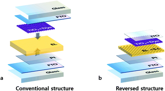
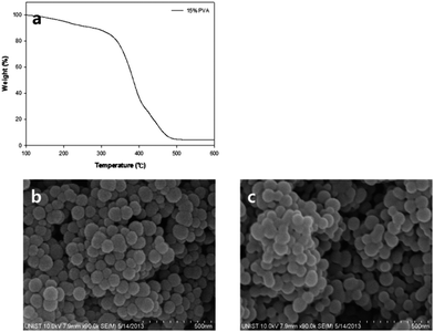
The schematic structures of reversed (RS-DSSC) and conventional DSSCs are presented in Fig. 1. Most of the DSSCs conventionally employ sandwich structures with two electrodes facing each other (Fig. 1a). Unlike the conventional structures, a RS-DSSC can be fabricated on a Pt-coated counter electrode as substrate from the bottom. Thin supporting layer and TiO2 photo anode were positioned on the substrate in turn, and the ITO layer was applied as TCO on the top of structures. Not only to prevent direct contact of the electrodes but also electrolyte penetration, porous supporting layer was inserted between the two electrodes.Fig. 2a shows the thermogravimetric analysis (TGA) curves of prepared supporting layer paste. Up to 300 °C, the TGA shows a gradual curve which indicates that the residues still exist. However, it also shows drastic weight loss starting at 350 °C, possibly due to the combustion of PVA. In order to facilitate dye adsorption and electrolyte penetration, the inner pore size should be sufficiently big to avoid the inferior aggregation. Fig. 2b and c show the morphology of supporting layer investigated using scanning electron microscopy after sintering at 450 °C and 500 °C, respectively. 450 °C sintering shows better surface morphology than 500 °C with inferior aggregation.
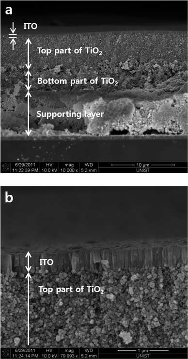
Fig. 3 represents the crosssectional morphology of the supporting layer, TiO2 and ITO layer which were formed in sequence. The supporting layer was made on a Pt coated FTO with an average thickness of 6 μm and 2 different compositions of TiO2 nanoparticles were pasted. The top part of 20 nm sized TiO2 nanoparticles with a thickness of 5 μm is the main active layer, while the bottom part of TiO2 which was mixed 20 nm and 500 nm nanoparticles 4 μm thick improved the adhesion between the supporting and active layer. Not only does the bottom TiO2 act as an adhesion layer but also as a scattering layer. Even though the bottom part of TiO2 shows a photosynthesis properties, the surface should be secured the flatness for the sputtered TCO. Fig. 3b shows a zoomed view of the ITO. The evaporated ITO formed a continuous thin layer on top of the TiO2 nanoparticles with a thickness of 200 nm.
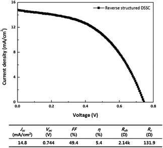
A complete RS-DSSC shows a short circuit current density (Jsc) of 14.8 mA cm−2, open circuit voltage (Voc) of 0.81 V, fill factor (FF) of 49.4% with power conversion efficiency (η) of 5.4% as shown in Fig. 4. It is well known that the short-circuit current density is mainly determined by the transfer of total number of photogenerated electrons to the electrode. Although the ITO layer was sputtered onto the TiO2, the observed results indicate that the RS-DSSC shows quite comparable values of Jsc to the conventional structure. However, the FF value is quite lower than the conventional structures. The J–V curve informs that the device has high series resistance and low shunt resistance. Since the ITO layer is prepared on rough TiO2 nanoparticles, its conductivity through lateral direction might exist. In addition, the contact between ITO and TiO2 nanoparticles needs to be investigated. Shunt resistance might be from ITO floating or TiO2 nanoparticle penetration through supporting layer, which can cause shorts.
In addition, in order to check the electron kinetics and investigate the interfacial properties,22 an electrochemical impedance spectroscopy (EIS) was employed which was performed under AM 1.5 front side illumination in an open-circuit voltage condition. Fig. 5 shows the measured EIS and the fitting parameters for the impedance spectroscopy of RS-DSSC were summarized in Table 1.
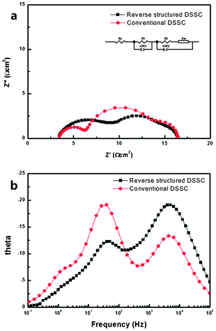 | ||
| Fig. 5 (a) Nyquist plot and (b) Bode phase plot of the electrochemical impedance spectroscopy of reverse structured DSSC. The equivalent circuit of the device is shown in the inset of (a). | ||
| R shunt (Ω) | R series (Ω) | R s (Ω cm2) | R ct1 (Ω cm2) | R ct2 (Ω cm2) | R diff (Ω cm2) | f max (Hz) | |
|---|---|---|---|---|---|---|---|
| RS-DSSC | 2.14k | 131.9 | 3.4 | 5.4 | 6.1 | 1.5 | 50.1 |
The equivalent circuit of this type of cell is described in the inset of Fig. 5a. Rs, CPE, R1 and R2 represent series resistance in high frequency region, constant phase element which was equivalent electrical circuit component, and resistances respectively. In Fig. 5a, the first semicircle at the high frequency is ascribed to the charge transfer at the interface between the counter electrode and electrolyte (Rct1), and the second semicircle at the middle frequency is associated with the charge transfer across the dye/TiO2/electrolyte (Rct2). The additional third semicircle is attributed mainly to the Nernst diffusion of I3− within the electrolyte (Rdiff). At the RS-DSSC structure, the supporting layer should be placed onto the Pt electrodes not only to make a room for electrolytes but also to form the photo-electrodes. Due to the direct contact of porous supporting layer and Pt electrode, the interface resistance can makes the larger first semicircle at the high frequency region than that of the conventional cells. Thus, the corresponding charge transfer resistance of RS-DSSC and conventional cells is 5.4 Ω cm2 and 3.1 Ω cm2 respectively. However, the charge transfer resistance of the RS-DSSC in the intermediate frequency region (Rct2) and the low frequency region (Rdiff) has the value of 6.1 Ω cm2 and 1.5 Ω cm2 respectively. These values are comparable to that of the conventional DSSC having Rct2 of 7.0 Ω cm2 and Rdiff of 2.0 Ω cm2 and their semicircles are more or less similar in shape. These results were also supported by the Bode plots in Fig. 5b. The fitted Bode plots display the frequency peaks of the various charge transfer processes at different interfaces. The electron recombination time could be calculated by τr = 1/(2πfmax) equation, where fmax corresponds to the highest frequency value of the peak in the bode plot. The RS-DSSC and conventional cells gave the fmax value of 39.81 Hz and 39.26 Hz respectively and the corresponding τr value was calculated as 4.0 ms for the RS-DSSC and 4.05 ms for the conventional cell. The τr in RS-DSSC is quite competitive with the conventional cell.
Conclusion
In summary, we have successfully fabricated RS-DSSC onto one substrate by controlling each layer. Even though the nanoparticle beads have incorporated in the reversely assembled structure, dye and electrolytes molecules could penetrate into the inner pore and a power conversion efficiency of 5.4% was achieved for the RS-DSSC with a similar Jsc and Voc values as of the conventional DSSCs. This technique could be extended to produce devices in research, including a flexible or a tandem solar cell with other thin film solar cells such as Cu(In, Ga)Se2 (CIGS) or organic photovoltaic devices.Acknowledgements
This publication is partially based on work supported by the Ministry of Science, ICT and Future Planning (2013069390, 2013K000204) and KETEP (20123010010070).Notes and references
- B. O'Regan and M. Gratzel, Nature, 1991, 353, 737–740 CrossRef CAS.
- M. Law, L. E. Greene, J. C. Johnson, R. Saykally and P. Yang, Nat. Mater., 2005, 4, 455–459 CrossRef CAS PubMed.
- Y. H. Jang, X. Xin, M. Byun, Y. J. Jang, Z. Lin and D. H. Kim, Nano Lett., 2012, 12, 479–485 CrossRef CAS PubMed.
- N. Yang, J. Zhai, D. Wang, Y. Chen and L. Jiang, ACS Nano, 2010, 4, 887–894 CrossRef CAS PubMed.
- Y. Jo, J. Y. Cheon, J. Yu, H. Y. Jeong, C. H. Han, Y. Jun and S. H. Joo, Chem. Commun., 2012, 48, 8057–8059 RSC.
- L. Kavan, J. H. Yum and M. Grätzel, ACS Nano, 2011, 5, 165–172 CrossRef CAS PubMed.
- J. Lim, S. Y. Ryu, J. Kim and Y. Jun, Nanoscale Res. Lett., 2013, 8, 1–5 CrossRef PubMed.
- Q. Miao, L. Wu, J. Cui, M. Huang and T. Ma, Adv. Mater., 2011, 23, 2764–2768 CrossRef CAS PubMed.
- H. P. Wu, Z. W. Ou, T. Y. Pan, C. M. Lan, W. K. Huang, H. W. Lee, N. M. Reddy, C. T. Chen, W. S. Chao, C. Y. Yeh and E. W. G. Diau, Energy Environ. Sci., 2012, 5, 9843–9848 CAS.
- J. Lim, M. Lee, S. K. Balasingam, J. Kim, D. Kim and Y. Jun, RSC Adv., 2013, 3, 4801–4805 RSC.
- S. K. Balasingam, M. Lee, M. G. Kang and Y. Jun, Chem. Commun., 2013, 49, 1471–1487 RSC.
- M. S. Wu, C. H. Tsai, J. J. Jow and T. C. Wei, Electrochim. Acta, 2011, 56, 8906–8911 CrossRef CAS PubMed.
- Y. Jo, C. L. Jung, J. Lim, B. H. Kim, C. H. Han, J. Kim, S. Kim, D. Kim and Y. Jun, Electrochim. Acta, 2012, 66, 121–125 CrossRef CAS PubMed.
- H. Wang, Y. Liu, H. Xu, X. Dong, H. Shen, Y. Wang and H. Yang, Renewable Energy, 2009, 34, 1635–1638 CrossRef CAS PubMed.
- K. Goto, T. Kawashima and N. Tanabe, Sol. Energy Mater. Sol. Cells, 2006, 90, 3251–3260 CrossRef CAS PubMed.
- C. Sima, C. Grigoriu and S. Antohe, Thin Solid Films, 2010, 519, 595–597 CrossRef CAS PubMed.
- I. Zumeta, J. A. Ayllón, B. González, X. Domenech and E. Vigil, Sol. Energy Mater. Sol. Cells, 2009, 93, 1728–1732 CrossRef CAS PubMed.
- M. Dürr, A. Schmid, M. Obermaier, S. Rosselli, A. Yasuda and G. Nelles, Nat. Mater., 2005, 4, 607–611 CrossRef PubMed.
- T. Miyasaka and Y. Kijitori, J. Electrochem. Soc., 2004, 151, A1767–A1773 CrossRef CAS PubMed.
- B. Yoo, K. Kim, S. H. Lee, W. M. Kim and N.-G. Park, Sol. Energy Mater. Sol. Cells, 2008, 92, 873–877 CrossRef CAS PubMed.
- J. H. Park, Y. Jun, H. G. Yun, S. Y. Lee and M. G. Kang, J. Electrochem. Soc., 2008, 155, F145–F149 CrossRef CAS PubMed.
- S. Ito, S. M. Zakeeruddin, P. Comte, P. Liska, D. Kuang and M. Grätzel, Nat. Photonics, 2008, 2, 693–698 CrossRef CAS.
Footnote |
| † These authors contributed equally to this work. |
| This journal is © The Royal Society of Chemistry 2014 |

