
 Open Access Article
 This Open Access Article is licensed under a
 Creative Commons Attribution 3.0 Unported Licence
The real TiO2/HTM interface of solid-state dye solar cells: role of trapped states from a multiscale modelling perspective†
Alessio
Gagliardi
*a,
Matthias
Auf der Maur
b,
Desiree
Gentilini
b,
Fabio
di Fonzo
c,
Agnese
Abrusci
d,
Henry J.
Snaith
d,
Giorgio
Divitini
e,
Caterina
Ducati
e and
Aldo
Di Carlo
b
aTechnische Universität München, Electrical and Computer Eng., Arcisstr. 21, 80333 München, Germany. E-mail: alessio.gagliardi@tum.de
bUniversity of Rome “Tor Vergata”, Via del Politecnico 1, 00133, Rome, Italy
cCenter for Nano Science and Technology of IIT@PoliMI, Via Pascoli 70/3, 20133 Milano, Italy
dUniversity of Oxford, Dep. of Physics, Clarendon Laboratory, Parks Road, Oxford OX1 3PU, UK
eUniversity of Cambridge, Dep. of Materials Science and Metallurgy, 27 Charles Babbage road, Cambridge CB3 0FS, UK
First published on 21st November 2014
Abstract
In this paper we present a multiscale simulation of charge transport in a solid-state dye-sensitized solar cell, where the real morphology between TiO2 and the hole transport material is included. The geometry of the interface is obtained from an electron tomography measurement and imported in a simulation software. Charge distribution, electric field and current densities are computed using the drift-diffusion model. We use this approach to investigate the electrostatic effect of trap states at the interface between the electron and hole transport materials. The simulations show that when the trapped electrons are not screened by external additives, the dynamics of holes is perturbed. Holes accumulate at the interface, enhancing recombination and reducing cell performance.
1. Introduction
Electronic technology has boomed in recent years mainly thanks to the enormous amount of research on materials science. A new class of materials is therefore emerging, i.e. organic semiconductors, which has opened interesting perspectives for electronic and optoelectronic devices.1–3 Organic semiconductors are becoming a crucial component for photovoltaic devices as well, where they can play either the role of active layer, as in organic photovoltaic cells (OPV),4 or hole transporter material, as in solid-state dye-sensitized solar cells (ss-DSCs).5 ss-DSCs have evolved from dye solar cells (DSCs),6,7 electrochemical photovoltaic devices that use a mesoporous oxide, usually titanium oxide (TiO2), sensitized with a monolayer of molecules, the dye, to convert light into electricity. The TiO2 acts as an electron transport layer, while the dye is the active component that absorbs light. In standard DSCs, the role of hole transport layer is played by a liquid electrolyte containing a redox couple. However, several engineering problems plague DSCs, such as the integrity of the liquid electrolyte. In fact, contamination from the external atmosphere or escaping of the electrolyte from microcracks within the sealant cause the efficiency of the cell to deteriorate over time, shortening the device’s lifespan. Finding a good sealant for DSCs is still an open problem.8 For this reason the liquid hole transporter has been replaced with a solid one5 using both small molecule (such as 2,2′,7,7′-Tetrakis-(N,N-di-4-methoxyphenylamino)-9,9′-spirobifluorene (Spiro-OMeTAD)) or polymer (such as Poly(3-hexylthiophene-2,5-diyl) (P3HT)) organic semiconductors.9 Recently discovered perovskite solar cells have also emerged from DSC technology, starting from an effort to replace the dye10 and the hole transporter.11The first prototypes of ss-DSCs had limited efficiency, but it was rapidly realized that the efficiency could be enhanced by doping the hole transport material with ionic additives such as lithium bis(trifluoromethylsulfonyl)-imide (Li-TFSI) in Spiro-OMeTAD.12 The ionic additives are known to change many aspects of the bulk properties of the organic material as well as its interface characteristics. For example it is known that dopants change the density of holes,13 but also the hole-hopping mobility by smoothing the electrostatic landscape and easing the hopping process.14–16 They modify the optical properties of the dye,17,18 altering band alignment between TiO2 and the hole transport material by creating a dipole moment at the interface.19 Despite an intense investigation, many aspects of the doping are not completely clear in a working ss-DSC device, considering the complex interplay between many different processes affected by the dopants, which change the cell performance. For example, it has been demonstrated13 that increasing the concentration of dopant Li-TFSI beyond 10% molarity does not further improve the efficiency of the cell, but still increases the fill factor (FF), suggesting that the dopants induce different effects that could also work in opposite directions.
The effect on the interface has been studied in detail and several aspects have been identified: one is the formation of a dipole moment, which shifts down the vacuum level of the TiO2,19 the other is the effect of intercalation of lithium ions in the oxide, which induces an increase in electron trap states and a lower diffusivity of negative charges.20–22 Considering these last two effects, it would seem that adding ionic additives has mostly a bad influence on the cell. However, we should consider the determinant role of lithium ions in reducing the recombination.23 Several authors have pointed out that this is due to the presence of the positive lithium ions, which screen the electrostatic interaction between electrons and holes.24,25 Such screening is especially important between trapped electrons at the interface26,27 and holes in the hole transport material.
The investigation of these effects is very complex considering that in experimental measurements, which usually consider the entire device, it is very hard to decouple the different physical/chemical mechanisms involved. Thus, theory and simulations can be helpful in trying to isolate different processes and evaluate their impact on the overall efficiency of the cell. Theoretical investigations on ss-DSCs are generally focused on the coordination effect of these ionic additives28 and on the mobility of lithium ions.22 More recently, the effect of ionic additives on the hole conductivity of Spiro-OMeTAD has been assessed by means of a Kinetic Monte Carlo simulation.39 This allows to investigate from a more microscopic perspective the effect of additives on charge hopping by distinguishing between dopant additives (Li-TFSI, H-TFSI) and inactive additives, where no charge transfer occurs (Na-TFSI, Et4Na-TFSI). This study reveals the importance of electrostatic effects on hole conductivity induced by the introduction of an anion–cation pair in the organic matrix. Nevertheless, the gap between modelling of the whole device and experimental measurements is broad, and many questions are still open.
In particular, device modelling tends either to neglect nanoscale morphology by considering effective material properties or to assume highly idealized geometries.40 To assess the effect of the mesoscopic features of porous TiO2 in ss-DSC modeling, it is necessary to integrate information on the morphology into the simulation model. Such information can be obtained with high spatial resolution from electron tomography.41
In this work we present numerical simulations of charge transport in a working ss-DSC device, adopting an innovative multiscale approach to include the real interface between TiO2 and the hole transport material. We will focus on the electrostatic effect due to the interplay of ionic additives and electronic trap states at the interface. We consider two limiting cases. The first one concerns a cell without ionic additives, such that the electrostatics near the interface are governed by the charged traps. In the second case we assume a sufficiently high concentration of ionic additives, resulting in a complete screening of charged traps. In the latter case we consider only non-doping additives in order not to alter bulk properties, and we assume perfect screening with zero Debye length, such that the additives do not have to be included explicitly in the simulation model.
2. Modelling
Devices like DSCs pose a challenging problem for their modelling. The interface between the hole (HTM) and electron transport materials (ETM) is a fundamental part of the system, where most of the main processes (charge generation, recombination and trapping/detrapping events) occur. However, this interface is tortuous due to the nanoporous nature of the TiO2, and integration of the real interface in the simulation is very difficult, mainly due to two problems. The first concerns the difficulty in getting experimental measures of the actual geometry of such a complex structure. The second is related to the big difference in characteristic lengths between the mesoporous morphology (nm) and the thickness of the active layer of the device (μm): while the first is of the order of the diameter of the TiO2 nanoparticles used to form the mesoporous layer (15 nm), the second is in the range of a few micrometers, allowing the dye to absorb as much light as possible. The challenge is to handle the two different length scales within the same simulation. If in fact we describe the porous active layer with the resolution of the morphology, simulating the entire device is very computationally expensive since a large amount of information is needed to properly describe the exact interface geometry in the full volume of the solar cell. Commonly, this problem is overcome by using an effective material approximation.40 By effective material we mean that the real geometry of the interface is not included in the simulation. The electron and hole transport materials are treated as a single homogeneous material that fills the device. This effective material is parameterized using the ETM parameters for electrons and HTM parameters for holes. The main advantage of this approximation is that the complex structure of the interface is removed from the simulation model with a great simplification and reduction in computational cost. The characteristic length in this case reduces to the length of the active layer and thus it is in the range of micrometers. Moreover, it allows us to model the device even if the details of the morphology are unknown.The main drawback is that all the processes (generation, recombination, etc.) that occur at the interface must be now converted into bulk models. Passing from interface to bulk models introduces approximation in the recombination and generation and their parameters should be adjusted to take into account the change in device description. Moreover, some aspects about the operation of the device, especially the charge distribution close to the interface, are definitely lost in this approximation.
In this work we use an intermediate approach: we describe part of the device using the resolution of the morphology, while the rest of the active layer is simulated using an effective material approximation (see Fig. 1). This strategy allows us to model the entire system and thus to analyze the performance of the cell, being able at the same time to describe the real interface in at least one sub-part of the active layer.
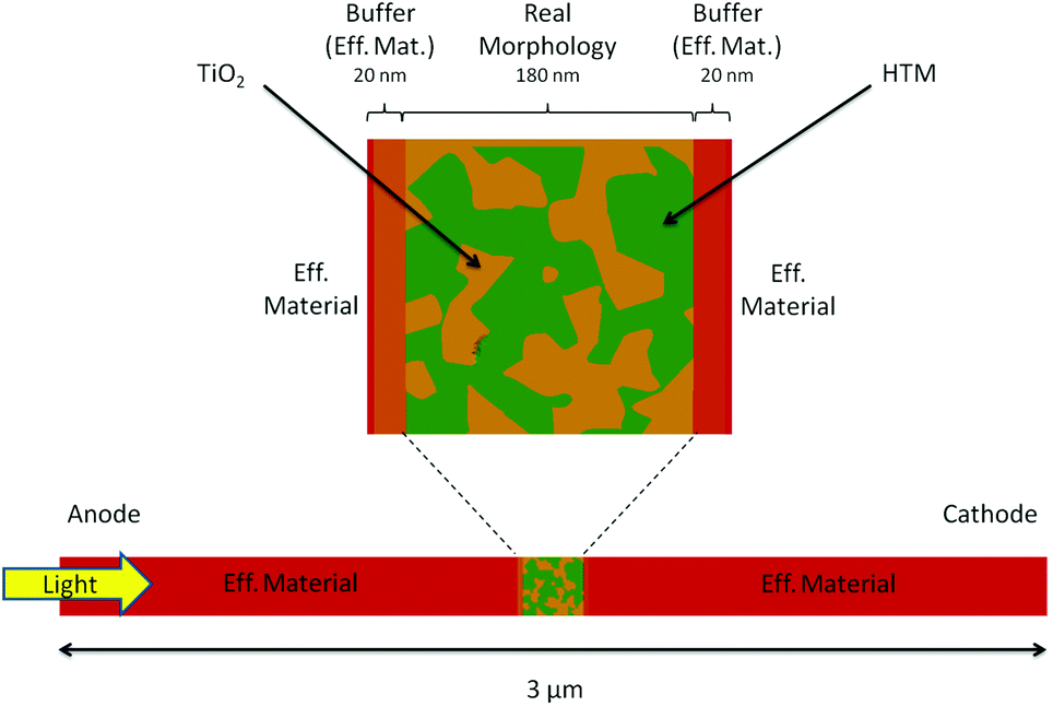 | ||
| Fig. 1 Embedding of the real morphology (central region) within two regions modelled using the effective material for a 2D device. The mesh is divided in five parts, two regions close to the contacts (anode and cathode) with a less dense meshing, two buffering regions at the interface with a denser meshing but still using the effective material, and a central region with a 2D slice of the real blend. The entire device is 3 μm long and the light comes from the left (anode) side. We assume periodic boundary conditions for the side boundaries of the cell. | ||
The morphology region has been constructed by using the experimental measurement of the interface geometry of a TiO2/Spiro-OMeTAD ss-DSC. The meshing of the full 3D structure is a challenging task and leads to the high computational cost of the transport simulations. Therefore, the geometry has been simplified considering a 2D slice of the real morphology (180 nm × 180 nm) embedded in two regions using the effective material. This dimensional reduction is not a too restricitve approximation, as it can still address the problem of local charge distribution and the interplay between free and trapped charges at the interface.
The numerical simulations are based on the drift-diffusion (DD) equations and solved using the finite element method (FEM), using the TiberCAD simulation tool.29–31 The finite element approach is particularly suited since it allows us to easily discretize complex geometries. DSCs are generally simulated in a 1D domain32–35 solving the diffusion equation only, considering that, especially for standard DSCs with liquid electrolyte, the long-range electric field is screened. Several attempts to analyze the system, including for example the electrostatic potential or going beyond the 1D approximation, have been performed.36 Other studies have investigated a complete DSC including the electrolyte, studying 2D37 and 3D44–46 effects or innovative architectures.47
In DD the current is calculated by coupling the constitutive equations for charge transport with the continuity equation for charge conservation:
| ∇(μne(h)∇ϕe(h)) = G − R, | (1) |
| εΔϕ = −ρ, | (2) |
The system under investigation is a mix of TiO2 as ETM and Spiro-OMeTAD as HTM. The two materials have very different transport properties. In fact, even if the TiO2 is made of sintered nanoparticles, the electron transport can be approximated to charge transport in a crystalline system, with a well-defined conduction band edge and the approximation of parabolic density of states close to the bottom (top) of the conduction (valence) band. On the contrary, the organic material charge transport is based on the transport of polarons and their hopping between adjacent molecules or available energy states. The density of states (DOS) of an organic semiconductor is described by a Gaussian DOS where the center of the Gaussian for the conduction band is levelled to the LUMO (lowest unoccupied molecular orbital) of the molecular/polymeric species and for the valence band to the HOMO (highest occupied molecular orbital):
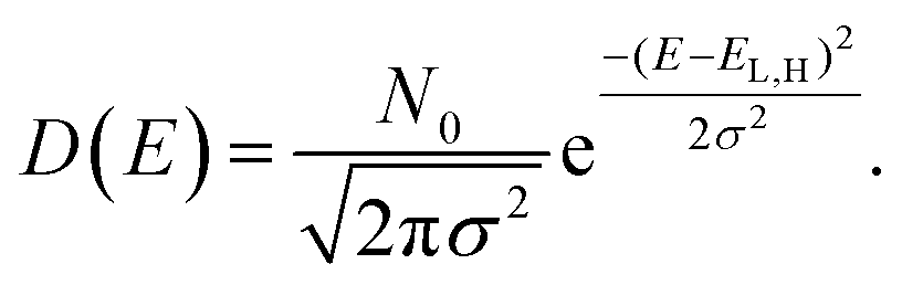 | (3) |
In eqn (3)N0 is the number of energy sites per cm3, σ2, the energy variance, is a function of the disorder of the organic material, and EL(H) is the LUMO (HOMO) energy level. This approximation for organic semiconductors is correct in the non-degenerate case, when the quasi-Fermi levels are within the energy gap and what defines the density are the tails of the Gaussian DOS. The charge density can be calculated from the DOS by assuming a local thermodynamic equilibrium and a quasi-Fermi level and Fermi–Dirac distribution.
3. Parameterization
The simulation of the cell requires a careful parameterization of the materials and their electrical properties. Considering the structure, shown in Fig. 1, we need a different parameterization for the HTM, the ETM and the effective material. These parameterizations are not independent, because the effective material is an approximation of the real morphology for the distinct HTM and ETM. In the present work, TiO2 parameters are taken from ref. 48, apart from the recombination constant, while those of Spiro-OMeTAD are gathered from literature as reported in Tables 1 and 2. Parameters for the effective material are reported in Table 3.| Parameter | Symbol | TiO2 | Units |
|---|---|---|---|
| Electron mobility | μ e | 0.5 | cm2 V−1 s−1 |
| Hole mobility | μ h | 0.5 | cm2 V−1 s−1 |
| Density of states (CB) | N c | 2.51 × 10¹⁹ | cm−3 |
| Density of states (VB) | N v | 3.25 × 10¹⁹ | cm−3 |
| Energy gap | E g | 4.2 | eV |
| Relative dielectric const. | ε r | 85 | |
| Rec. constant (interface) | C 0 | 2 × 10⁻¹⁵ | cm2 s−1 |
| Trap density (interface) | N t | 1013 | cm−2 |
| Trap dens. exponent | a | 0.3 |
| Parameter | Symbol | Spiro-OM. | Units |
|---|---|---|---|
| Electron mobility | μ e | 0.001 | cm2 V−1 s−1 |
| Hole mobility | μ h | 0.001 (ref. 39) | cm2 V−1 s−1 |
| Density of states (CB) | N c | 1019 (ref. 38) | cm−3 |
| Density of states (VB) | N v | 1019 | cm−3 |
| Energy disorder (CB) | σ e | 65 (ref. 38) | meV |
| Energy disorder (VB) | σ h | 65 (ref. 38) | meV |
| Energy gap | E g | 2.98 (ref. 42) | eV |
| Relative dielectric const. | ε r | 3.53 | |
| Rec. constant (interface) | C 0 | 2 × 10⁻¹⁵ | cm2 s−1 |
| Trap density (interface) | N t | — | cm−2 |
| Trap dens. exponent | a | — |
| Parameter | Symbol | Eff. medium | Units |
|---|---|---|---|
| Electron mobility | μ e | 0.5 cm2 V−1 s−1 | |
| Hole mobility | μ h | 0.001 | cm2 V−1 s−1 |
| Density of states (CB) | N c | 2.51 × 10¹⁹ | cm−3 |
| Density of states (VB) | N v | 1019 | cm−3 |
| Energy disorder (VB) | σ h | 65 | meV |
| Energy gap | E g | 1.3 (ref. 42 and 43) | eV |
| Relative dielectric const. | ε r | 36.52 | |
| Rec. constant (bulk) | C | 2 × 10⁻¹⁰ | cm3 s−1 |
| Trap density (bulk) | N t | 1019 | cm−3 |
| Trap dens. exponent | a | 0.3 |
A specific discussion is required for the parameterization of recombination/generation models and trap density at the interface. These three models are the only ones that change passing from the real morphology where they are related to interface processes, to the effective material where they are related to bulk processes.
Recombination is a fundamental issue for defining the performance of the ss-DSC. For the cell a direct recombination rate of the form:
| R = C0(nenh − ni2), | (4) |
The same recombination rate equation is used both in the effective material region and in the real morphology one. The main difference is that in the first case it is a bulk process, in the second it is a surface recombination. This means that even if the recombination equation is the same, the recombination constant cannot be the same, and also because the dimensionality of the constant is not equal in the two cases (cm3 s−1 in the bulk, cm2 s−1 in the surface case).
Generation is modelled with the Lambert–Beer equation. The thickness of the active region is long enough that standing waves effects will not occur as happens for organic solar cells. The generation is defined as:
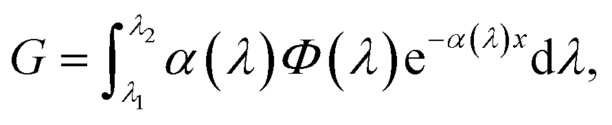 | (5) |
Also in this case, as for the recombination term, generation is treated differently passing from the effective material to the real morphology regions. In the real morphology region, we assume a constant generation rate. This approximation can be made considering that the thickness of this region is much smaller compared to the absorption length of N719 (around 0.1–0.2 μm). After generation electrons are collected by the ETM and holes by the HTM.
The contacts are modelled as Mott–Schottky contacts, where the injection barriers are kept very small (0.3 eV between conduction band/HOMO level and contact Fermi energy) and with an efficient injection velocity. We assume that contacts offer a negligible resistance and that the device is limited mainly by bulk recombination.
At the interface between the two materials a density of trap states is also present.27 Trap states are modelled with a surface exponential density:
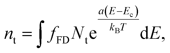 | (6) |
4. Merging the effective and the real morphology models
The concurrent multiscale simulation of the effective and real morphology regions is a delicate issue. The challenge is how to define consistent parameters for the two regions avoiding spurious effects such as charge accumulation or electric fields at the interfaces between the two regions. A simple scheme has been developed to solve this issue: parameters for the real morphology region have been chosen in order to assure that the total recombination and generation in the real morphology region and in an equivalent area using the effective model were the same, i.e. | (7) |
 | (8) |
In eqn (7) and (8) the first integral is over a volume with the effective medium approximation (VEM), while the second along the interface (SRM) between ETM and HTM with the real morphology.
The results have been checked by calculating the J–Vs with and without trap states at the interface using the effective material (EM) or the real morphology (RM) descriptions (see Fig. 2). A small offset is present for Jsc and Voc, the first is more evident without trap states, while the second is particularly present with trap states. The offset in the short circuit current is due to the approximation in the constant generation model for the RM region, as discussed previously. The difference in open circuit voltage when trap states are considered is induced by the different modelling between RM and EM, as discussed in the next section. The J–Vs shown in Fig. 2 present very low efficiency. This is due to the fact that the configuration with traps is a pristine ss-DSC, i.e. a solid state cell where no treatment using the additives has been performed. Also, in the second simulation, with no trap states, we are not considering a fully-functioning ss-DSC, as not all the effects of the additives have been included in the model. Moreover, the dye used as a light absorber, the N719, is not the best for a ss-DSC due to the limitations in active layer thickness (2 or 3 μm) in these devices concurrent with the poor molar extinction coefficient of N719.51 For this reason other dyes, such as C104 or Z907, are usually used.
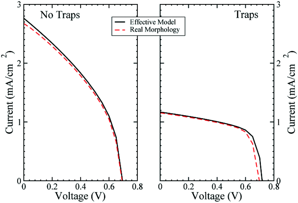 | ||
| Fig. 2 (Left) J–V characteristics without trap states at the interface with and without real morphology in the middle of the cell. (Right) the same as in the left but adding the trap states at the interface. | ||
As a consistency check to assure that inserting the RM region is not modifying the physics of the device, we have compared the band bending for a pure EM device with that of the device with the RM region added, for different working points and varying the location of the RM region inside the active layer (in the middle, close to the anode or to the cathode). In Fig. 3 the results for the cases close to the anode and the cathode are shown. The conduction and valence bands of the TiO2 and the HOMO and LUMO levels for the organic semiconductor are plotted as well as the quasi-Fermi energy levels, showing both the EM and RM. The agreement between the two models is extremely accurate.
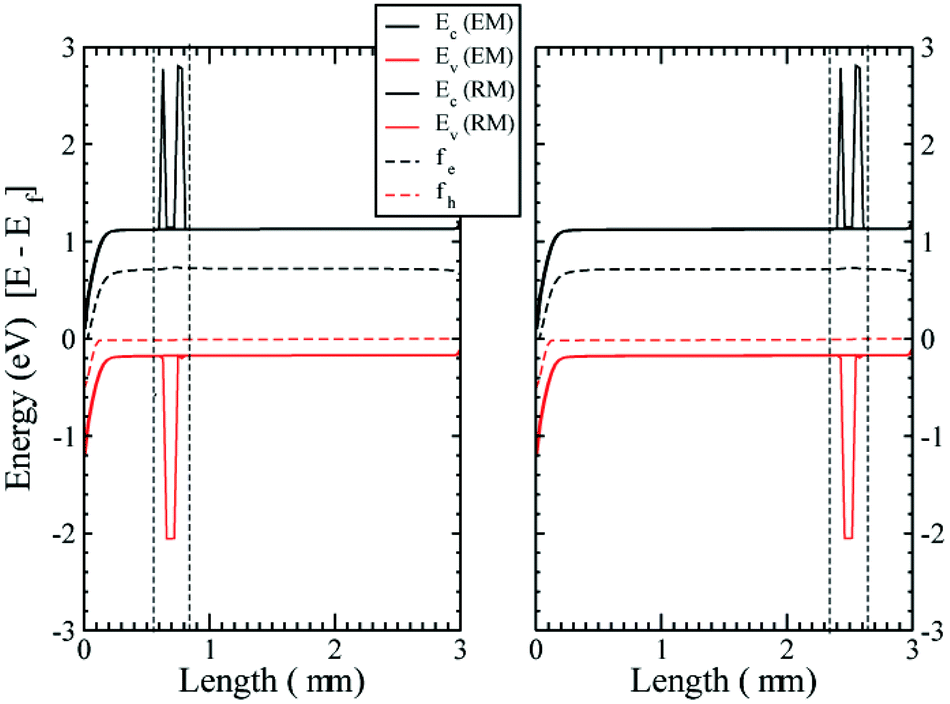 | ||
| Fig. 3 Conduction and valence bands (LUMO and HOMO level for the HTM) Ec and Ev and electrochemical potentials for electrons ϕe and holes ϕh at Jsc for different positions of the RM region. Close to the anode (left) and close to the cathode (right). The band bending is compared to calculations using the effective approximation (EM) only. The RM region is delimited by the vertical broken lines. | ||
5. Experimental measurements
The real geometry of the TiO2 for a portion of a ss-DSC has been reconstructed using an electron tomography dataset with high spatial resolution41 (see Fig. 4, top and (a)). In this approach, a transmission electron microscope (TEM) sample is cut out from a ss-DSC using focused ion beam milling (in a FEI Helios Nanolab) employing an annular geometry, resulting in a needle-shaped sample.52,53 The needle is lifted out from the device and attached to a TEM-compatible support; further annular thinning is finally employed until the sample is electron-transparent (around 150–200 nm). This choice presents an important advantage compared to the more established approach of extracting a flat lamella: the cylindrical symmetry ensures that the thickness of the sample doesn't increase while tilting, therefore the image quality of the dataset does not degrade for high tilt angles. A tilt series is then acquired in the TEM (FEI Titan operated at 200 kV in STEM mode, tilt range −76 → +76°), from which a 3D reconstruction can be computed. The image was used to process the reconstructed dataset, subtracting the background and applying a threshold for segmentation, isolating the TiO2 volume. Accurate, nanoscale morphological information can thus be retrieved. This allows direct imaging and 3D analysis of both the nanostructured TiO2 network and the HTM component (see Fig. 4).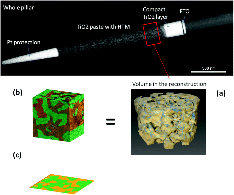 | ||
| Fig. 4 (Top) High angle annular dark field (HAADF) STEM image. (a) Reconstruction of the TiO2 morphology in a portion of the active layer. (b) Meshing of a cube extracted from the measurement of the TiO2, reconstructing the HTM phase. (c) 2D slice of the 3D morphology. | ||
6. Effect of traps at the surface of TiO2 mesoporous material on device performance
The relevance of trapped electrons at the interface between the ETM and HTM is extremely important27 and it is one of the reasons for the introduction of ionic additives in the preparation of ss-DSCs.24,25 The positive cations of the ionic additives can in fact screen the trapped electrons, changing the electrostatics in the active layer, especially in the HTM due to the lower permittivity of the organic semiconductor compared to the TiO2.This problem is less severe in standard DSCs, where the liquid electrolyte and high density of ions screen the trapped electrons. The cations accumulate at the interface, screening the electric field within a few ionic layers.54
On the contrary, in the case of a ss-DSC, no positive charges are available for the role of screening electrons at the interface, unless directly using the photogenerated holes. This is detrimental for the device operation, considering that the holes contribute to the photocurrent and any perturbation to their distribution could result in a reduction in cell efficiency.
To investigate the effect of trapped electrons we have performed several simulations in the multiscale geometry, including and not including the trap density of states at the interface. These two cases can be considered as limiting cases for an ss-DSC without and with ionic additives, respectively.
We have first investigated the role of trapped charges in an EM approximation (see Fig. 5). The figure shows the free electrons and holes profiles in the cell at Voc. The density of free electrons is reduced in the presence of trap states. The reason for this is that most of the electrons are trapped. The electron quasi-Fermi energy is positioned in the gap and then intercepts the exponential band tail of trap states below the conduction band. Thus, the fraction of trapped electrons is far larger than that of free carriers in the conduction band.
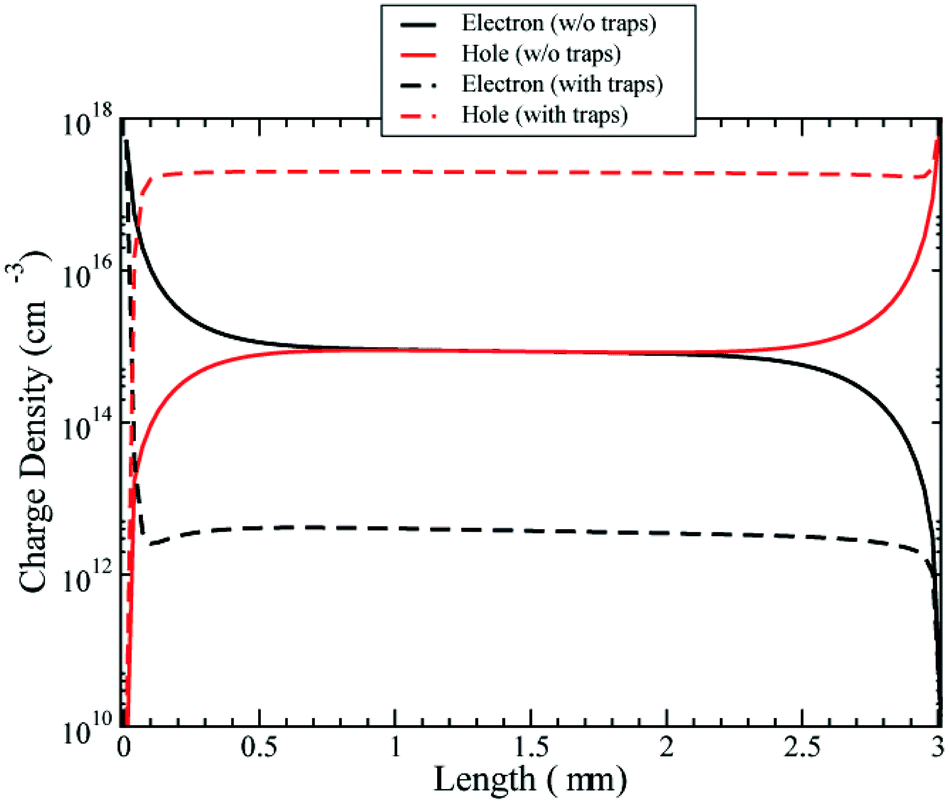 | ||
| Fig. 5 Density of electrons and holes with and without the presence of trap states at Voc. Effective model only. | ||
The density of holes is instead increased by the presence of trap states. The negative charge of the trapped electrons attracts holes in the active layer, increasing the equilibrium density. So the overall effect of trap states is to increase hole conductivity and reduce the electron conductivity.
The increase in hole density has a second effect, shown in Fig. 6. The figure presents the conduction, valence and quasi-Fermi energy levels for a cell with and without trap states. The simulations are performed at Jsc and a RM region is included in the middle of the active layer. In the figure it is clearly shown that the different charge density induced by traps changes the band bending in the cell, passing from a pronounced band bending especially close to the cathode (Fig. 6, left) to a flat band situation (Fig. 6, right). The band bending is the signature of a long-range electric field in the active layer. The disappearance of the electric field when trapped electrons are present limits the current (Fig. 2) as the electric field helps charge collection. The presence of a long-range electric field across the active layer in ss-DSCs is under debate. Experimental evidence using impedance spectroscopy points to a purely diffusion-based transport of charge carriers. This could be induced by one of the other effects produced by ionic additives, i.e. the doping of the HTM. However, from our simulations it is clear that the disappearance of a long-range electric field is detrimental to the device operation and that its screening should be considered as a negative effect.
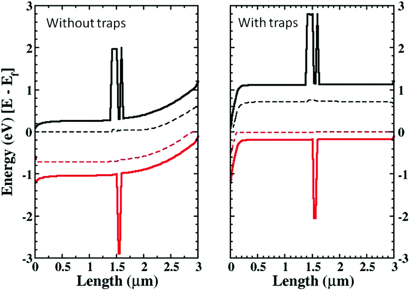 | ||
| Fig. 6 Effect of band bending at Jsc without (left) and with (right) charged trap states. | ||
It is known that ionic additives also reduce the interface recombination.23 We use the multiscale approach, including the RM in the active layer, to analyze the charge and current distribution in the active layer in more detail. In Fig. 7 the hole and current density at Jsc conditions are shown for the RM region with and without trapped electrons at the interface. The RM region is inserted close to the cathode contact.
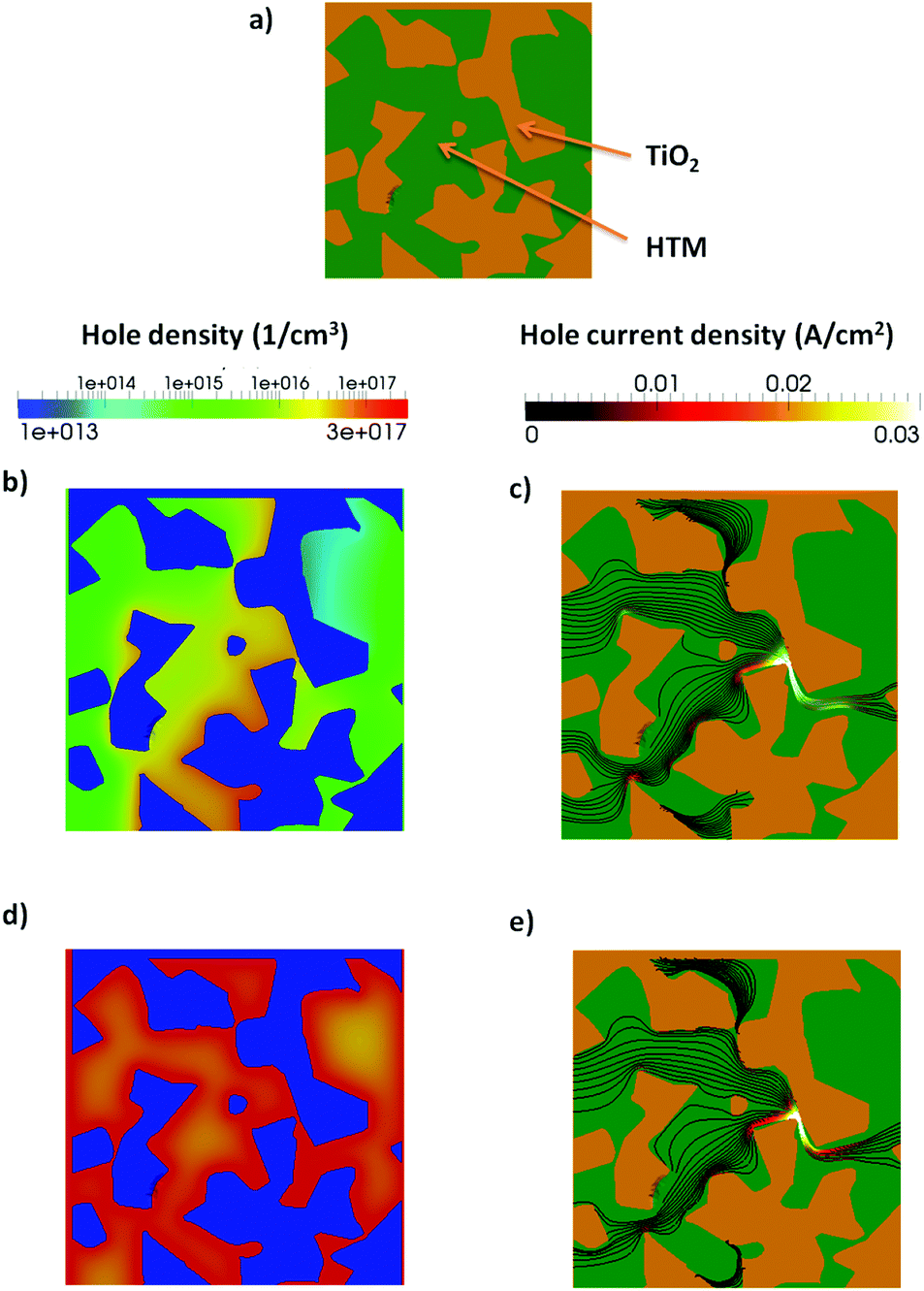 | ||
| Fig. 7 (a) The RM region with the TiO2 (orange) and the Spiro-OMeTAD (green). (b) Hole density and (c) hole current density at Jsc for the case without trapped electrons at the TiO2/HTM interface. (d) and (e) are the same as (b) and (c) but with trapped electrons at the interface. | ||
When trapped electrons are present the photogenerated holes accumulate at the interface due to electrostatic attraction. Considering that the recombination at the interface is proportional to the density of electron and holes, a higher density of holes implies a higher recombination. This effect is partially compensated by the lower density of free electrons. Moreover, the current of holes in the presence of traps (Fig. 7e) flows closer to the interface between the two materials. The higher recombination current is particularly evident in the bottleneck of the morphology.
The screening of the local electric field in the RM is shown in Fig. 8. This electric field is particularly intense where trap states are present. Differently from the long range, this local electric field is confined close to the interface and it is more intense in the organic semiconductor due to the lower permittivity.
 | ||
| Fig. 8 Electric field distribution inside the RM region at Jsc. (Left) without trapped electrons, (right) with trapped electrons. | ||
The analysis of the real morphology can indicate the strengths and weaknesses and the limits of the effective medium approximation. In particular we have pointed out how the effective medium strongly simplifies the real charge and current distribution inside the two materials, failing in properly describing the electrostatics at the interface. Effects of the morphology, especially if the electron percolation in the TiO2 is difficult, are necessarily lumped into the working parameters in an effective material approximation making their physical interpretation more problematic.
7. Conclusion
In the present work we have analyzed the effect of trap states at the interface in the mesoporous material of a ss-DSC. The electron and hole transport materials were TiO2 and Spiro-OMeTAD, respectively. In order to investigate the effect of charged trap states inside the active layer, two different models have been simulated: one using the effective material approximation, the other inserting in a sub region of the cell the real morphology of the mesoporous material. The geometry for the real morphology part was extracted by electron tomography measurements of a real ss-DSC. The insertion of the real morphology region allows us to describe with unprecedented accuracy the electrostatics between electrons and holes and charged trap states at the interface between electron and hole transport materials. The effective material model can in fact only account for the average distribution of charges and electrostatic potential because the real interface is not included.The simulations show the effect of charged trap states, which induce a higher density of holes in the active layer. The interplay between trapped electrons and holes screens all long-range electric fields, which is detrimental for the cell performance. Introducing a screening mechanism for trapped electrons, the long-range electric field is restored and current increases. The internal electric field in fact helps electrons and holes to reach the correct electrodes, improving the charge collection.
It is known that screening trapped electrons is one of the effects of ionic additives added to the organic semiconductor during the cell preparation. However, experimental measurements using impedance spectroscopy indicate that the transport of photogenerated charges is diffusive, an effect due to the doping of the organic material. Thus, even if the screening of the trapped electrons will restore the long-range electric field, some other effects of the additives prevent its presence. It is anyway clear that the presence of a long-range electric field in the active layer would increase the efficiency of the cell.
Analyzing in more detail the region with the real morphology, another effect becomes evident: the presence of electrons trapped at the interface attracts holes, which accumulate in a thin layer close to the interface. This produces a shift of the hole current close to the interface and enhances recombination. This effect disappears if trapped electrons are not present. A reduction in recombination after the adding of ionic additives has indeed been experimentally observed, and our results point out that the observed electrostatic effect and hole accumulation can be at the base of the experimental recombination modulation with and without ionic additives. These electrostatic effects are particularly important in the hole transport material due to the low permittivity of the organic semiconductor.
The last consideration is about the validity of the effective material model, an approximation widely used for ss-DSCs, but also for other devices like organic photovoltaic cells. Our simulations show that despite the fact that the effective medium approximation can be a valid tool to study devices with complex morphologies, it makes severe approximations in the real distribution of charges and current in the active layer. It just calculates an average value of these quantities. For high performance devices, with no percolation problem in the TiO2, the effective material model is a reasonable approximation of the real system. Its validity decreases rapidly if transport is limited by morphology reasons, in that case an effective material model is forced to include the morphology effects in its transport parameters.
References
- Z. Wang, M. Helander, J. Qiu, D. Puzzo, M. Greiner, Z. Hudson, S. Wang, Z. Liu and Z. Lu, Nat. Photonics, 2011, 5, 753–757 CrossRef CAS.
- D. T. McQuade, A. H. Hegedus and T. M. Swager, J. Am. Chem. Soc., 2000, 122, 12389–12390 CrossRef CAS.
- M. McCarthy, B. Liu, E. Donoghue, I. Kravchenko, D. Kim, F. So and A. Rinzler, Science, 2011, 332, 570 CrossRef CAS PubMed.
- H. Spanggaard and F. C. Krebs, Sol. Energy Mater. Sol. Cells, 2004, 83, 125–146 CrossRef CAS PubMed.
- U. Bach, D. Lupo, P. Comte, J. E. Moser, F. Weissaertel, J. Salbeck, H. Spreitzer and M. Grätzel, Nature, 1998, 395, 583–585 CrossRef CAS PubMed.
- A. Yella, H. W. Lee, H. N. Tsao, C. Yi, A. K. Chandiran, M. K. Nazeeruddin, E. W. G. Diau, C. Y. Yeh, S. M. Zakeeruddin and M. Grätzel, Science, 2011, 334, 629–634 CrossRef CAS PubMed.
- B. O'Regan and M. Grätzel, Nature, 1991, 353, 737–740 CrossRef.
- R. Sastrawan, J. Beier, U. Belledin, S. Hemming, A. Hinsch, R. Kern, C. Vetter, F. Petrat, A. Prodi-Schwab, P. Lechner and W. Hoffmann, Sol. Energy Mater. Sol. Cells, 2006, 90, 1680–1691 CrossRef CAS PubMed.
- F. Matteocci, G. Mincuzzi, F. Giordano, A. Capasso, E. Artuso, C. Barolo, G. Viscardi, T. M. Brown, A. Reale and A. Di Carlo, Org. Electron., 2013, 14(7), 1882–1890 CrossRef CAS PubMed.
- A. Kojima, K. Teshima, Y. Shirai and T. Miyasaka, J. Am. Chem. Soc., 2009, 131(17), 6050–6051 CrossRef CAS PubMed.
- P. Docampo, J. M. Ball, M. Darwich, G. E. Eperon and H. J. Snaith, Nat. Commun., 2013, 4, 2761 Search PubMed.
- H. J. Snaith and M. Grätzel, Appl. Phys. Lett., 2006, 89, 262114 CrossRef PubMed.
- A. Abate, T. Leijtens, S. Pathak, J. Teuscher, R. Avolio, M. E. Errico, J. Kirkpatrik, J. M. Ball, P. Docampo, I. McPherson and H. J. Snaith, Phys. Chem. Chem. Phys., 2013, 15, 2572–2579 RSC.
- J. Xia, N. Masaki, M. Lira-Cantu, Y. Kim, K. Jiang and S. Yanagida, J. Am. Chem. Soc., 2008, 130, 1258–1263 CrossRef CAS PubMed.
- D. A. R. Barkhouse, H. E. Bishop, B. M. Henry, G. R. Webster, P. L. Burn and H. E. Assender, Org. Electron., 2009, 11, 649–657 CrossRef PubMed.
- D. Bi, F. Wu, W. Yue, Q. Qu, Q. Cui, Z. Qiu, C. Liu, W. Shen and M. Wang, Sol. Energy, 2011, 85, 2819–2825 CrossRef CAS PubMed.
- A. Abrusci, I. K. Ding, M. Al-Hashimi, T. Segal-Peretz, M. D. McGehee, M. Heeney, G. L. Frey and H. J. Snaith, Energy Environ. Sci., 2011, 4, 3051–3058 CAS.
- U. B. Cappel, A. L. Smeigh, S. Plogmaker, E. M. J. Johansson, H. Rensmo, L. Hammarstrom, A. Hagfeldt and G. Boschloo, J. Phys. Chem. C, 2011, 115, 4345–4358 CAS.
- Q. Wang, Z. Zhang, S. M. Zakeeruddin and M. Grätzel, J. Phys. Chem. C, 2008, 112, 7084 CAS.
- N. Kopidakis, K. D. Benkstein, J. Van de Lagemaat and A. J. Frank, J. Phys. Chem. B, 2003, 107, 11307–11315 CrossRef CAS.
- P. Tiwana, P. Docampo, M. B. Johnston, L. Herz and H. J. Snaith, Energy Environ. Sci., 2012, 5, 9566 CAS.
- F. Fabregat-Santiago, J. Bisquert, L. Cevey, P. Chen, M. Wang, S. M. Zakeeruddin and M. Grätzel, J. Am. Chem. Soc., 2009, 131, 558–562 CrossRef CAS PubMed.
- J. Kreuger, R. Plass, L. Cevey, M. Piccirelli, M. Gratzel and U. Bach, Appl. Phys. Lett., 2001, 79, 2085 CrossRef PubMed.
- C. A. Kelly, F. Farzad, D. W. Thompson, J. M. Stipkala and G. J. Meyer, Langmuir, 1999, 15, 7047–7054 CrossRef CAS.
- T. Daeneke, A. J. Mozer, T. H. Kown, N. W. Duffy, A. B. Holmes, U. Bach and L. Spiccia, Energy Environ. Sci., 2012, 5, 7090 CAS.
- I. Mora-Sero and J. Bisquert, Nano Lett., 2003, 3, 945–949 CrossRef CAS.
- M. C. Fravventura, D. Deligiannis, J. M. Schins, L. D. A. Siebbels and T. J. Savenije, J. Phys. Chem. C, 2013, 117, 8032 CAS.
- D. Kuang, C. Klein, H. J. Snaith, J.-E. Moser, R. Humphry-Baker, P. Comte, S. M. Zakeeruddin and M. Grätzel, Nano Lett., 2006, m6, 769 CrossRef PubMed.
- M. Auf der Maur, G. Penazzi, G. Romano, F. Sacconi, A. Pecchia and A. Di Carlo, IEEE Trans. Electron Devices, 2011, 58, 1425 CrossRef.
- A. Gagliardi, S. Mastroianni, D. Gentilini, F. Giordano, A. Reale, T. Brown and A. Di Carlo, IEEE J. Sel. Top. Quantum Electron., 2010, 16, 1611 CrossRef CAS.
- A. Gagliardi, D. Gentilini and A. Di Carlo, J. Phys. Chem. C, 2012, 116, 23882–23889 CAS.
- P. R. F. Barnes, A. Y. Anderson, J. R. Durrant and B. C. O'Regan, Phys. Chem. Chem. Phys., 2011, 13, 5798–5816 RSC.
- F. Cappelluti, S. Ma, D. Pugliese, A. Sacco, A. Lamberti, G. Ghione and E. Tresso, Phys. Chem. Chem. Phys., 2013, 15, 14634–14646 RSC.
- J. A. Anta, J. Idgoras, E. Guilln, J. Villanueva-Cab, H. J. Mandujano-Ramrez, G. Oskam, L. Pellej and E. Palomares, Phys. Chem. Chem. Phys., 2012, 14, 10285–10299 RSC.
- J. Villanueva-Cab, G. Oskam and J. A. Anta, Sol. Energy Mater. Sol. Cells, 2010, 94, 45–50 CrossRef CAS PubMed.
- J. Ferber and J. Luther, J. Phys. Chem. B, 2001, 105, 4895–4903 CrossRef CAS.
- K. Miettunen, J. Halme, A. Visuri and P. Lund, J. Phys. Chem. C, 2011, 115, 7019 CAS.
- J. Garcia-Casidas, F. Fabregat-Santiago, H. J. Bolink, E. Palomares, G. Garcia-Belmonte and J. Bisquert, Synth. Met., 2006, 156, 944–948 CrossRef PubMed.
- A. Abate, D. R. Staff, D. J. Hollmann, H. J. Snaith and A. B. Walker, Phys. Chem. Chem. Phys., 2014, 16, 1132 RSC.
- A. Gagliardi, M. Auf der Maur, D. Gentilini and A. Di Carlo, J. Comput. Electron., 2009, 8, 398–409 CrossRef CAS.
- P. A. Midgley and R. E. Dunin-Borkowski, Nat. Mater., 2009, 8, 271 CrossRef CAS PubMed.
- T. Leijtens, I. Ding, T. Giovenzana, J. T. Bloking, M. D. McGehee and A. Sellinger, ACS Nano, 2012, 6, 1455–1462 CrossRef CAS PubMed.
- M. Wang, C. Grätzel, S.-J. Moon, R. Humphry-Baker, N. Rossier-Iten, S. M. Zakeeruddin and M. Grätzel, Adv. Funct. Mater., 2009, 19, 2163–2172 CrossRef CAS.
- A. Gagliardi, M. Auf der Maur and A. Di Carlo, IEEE J. Quantum Electron., 2011, 47, 1214 CrossRef CAS.
- A. Gagliardi, M. Auf der Maur, D. Gentilini and A. Di Carlo, J. Comput. Electron., 2011, 10, 424 CrossRef CAS.
- A. Gagliardi and A. Di Carlo, Opt. Quantum Electron., 2012, 44, 141–147 CrossRef CAS.
- R. Tagliaferro, D. Gentilini, S. Mastroianni, A. Zampetti, A. Gagliardi, T. M. Brown, A. Reale and A. Di Carlo, RSC Adv., 2013, 3, 20273 RSC.
- D. Gentilini, A. Gagliardi, M. Auf der Maur, L. Vesce, D. D’Ercole, T. M. Brown, A. Reale and A. Di Carlo, J. Phys. Chem. C, 2012, 116, 1151–1157 CAS.
- J. Halme, P. Vahermaa, K. Miettunen and P. Lund, Adv. Mater., 2010, 22(35), E210–E234 CrossRef CAS PubMed.
- J. Bisquert, A. Zaban and P. Salvador, J. Phys. Chem. B, 2002, 106(34), 8774–8782 CrossRef CAS.
- N.-G. Park, J. Phys. Chem. Lett., 2013, 4, 2423 CrossRef CAS.
- N. Kawase, M. Kato, H. Nishioka and H. Jinnai, Ultramicroscopy, 2007, 107, 8–15 CrossRef CAS PubMed.
- G. Divitini, et al. , Adv. Funct. Mater., 2014, 24, 3043–3050 CrossRef CAS.
- S. Nakade, T. Kanzaki, W. Kubo, T. Kitamura, Y. Wada and S. Yanagida, J. Phys. Chem. B, 2005, 109(8), 3480 CrossRef CAS PubMed.
Footnote |
| † Electronic supplementary information (ESI) available. See DOI: 10.1039/c4nr05208k |
| This journal is © The Royal Society of Chemistry 2015 |