An 80.11% FF record achieved for perovskite solar cells by using the NH4Cl additive†
Chuantian
Zuo
and
Liming
Ding
*
National Center for Nanoscience and Technology, Beijing 100190, China. E-mail: opv.china@yahoo.com
First published on 7th July 2014
Abstract
The light-absorbing perovskite layer fabricated using the NH4Cl additive shows high crystallinity and better morphology. The resulting solar cells gave a decent power conversion efficiency of 9.93% and a fill factor record of 80.11%. This work provides a very simple but effective approach to enhance the power conversion efficiency of perovskite solar cells.
Perovskite solar cells using organometal halide perovskites as light-absorbing materials have received a great deal of attention due to their excellent photovoltaic performance.1–4 CH3NH3PbX3 (X = Br, I) perovskite nanocrystals were used as sensitizers in dye-sensitized solar cells (DSSCs) and a power conversion efficiency (PCE) of 3.8% was obtained in 2009.5 Later, Park et al. reported an improved PCE of 6.54% by using CH3NH3PbI3 nanocrystals in DSSCs.6 In solid-state hybrid solar cells, PCEs of 10.9% and 9.7% were achieved when CH3NH3PbI2Cl and CH3NH3PbI3 were used as the absorbers, respectively.1,2 Recently, Wojciechowski et al. reported a 15.9% PCE in meso-superstructured perovskite solar cells.7 Perovskites are excellent semiconductors in solar cells due to their panchromatic light absorption, ambipolar transport and very long electron/hole diffusion lengths.8,9 A great deal of effort has been paid by researchers to explore this brand-new solar cell, e.g. developing low-temperature fabrication methods,4 making new hole conductors10 and trying flexible substrates.11
Perovskite solar cells with device structure indium tin oxide (ITO)/poly(3,4-ethylenedioxythiophene):polystyrene sulfonate (PEDOT:PSS)/perovskite/[6,6]-phenyl-C61-butyric acid methyl ester (PC61BM)/Al are becoming popular because they can be made into flexible devices and processed at 150 °C.11–16 Malinkiewicz et al. sandwiched sublimated CH3NH3PbI3 between the organic hole-transport layer and PC61BM, and obtained a 12% PCE.15 Lam et al. developed solution-processed CH3NH3PbI3/PC61BM solar cells and obtained a 5.2% PCE using a one-step deposition method and a 7.4% PCE using a sequential deposition method.13 Kim et al. improved the morphology of the CH3NH3PbI3 layer using solvent mixtures and obtained a PCE of 6.2%.16 The crystallinity and morphology of perovskite layers are very important for the performance of perovskite solar cells.16,17
Here, we report an innovative approach by using chloride additives to improve the crystallinity and morphology of perovskite layers, and the performance of solar cells. The effects of CH3NH3Cl and NH4Cl additives on the crystallinity and morphology of perovskite layers were studied. The additives helped to form flawless perovskite nanocrystals and also helped to form smooth and uniform films, leading to better device performance. A solution-processed device with the structure of ITO/PEDOT:PSS/CH3NH3PbI3/PC61BM/Al was studied. The device fabricated using NH4Cl as an additive gave a PCE around 10% and a fill factor (FF) over 80%.
The structure of CH3NH3PbI3/PC61BM solar cells is shown in Fig. 1. PC61BM is often used as an electron acceptor in organic solar cells and it can effectively quench the photoluminescence of perovskites in a bi-layer structure.18 So PC61BM can act as an electron acceptor and electron collection layer in perovskite solar cells. Under illumination, excitons generated in the perovskite layer will dissociate at the perovskite/PC61BM interface.14,18 Electrons move to the LUMO of PC61BM and are collected by the Al electrode. PEDOT is used as a hole-transport layer, holes move to the PEDOT layer and are collected by the ITO electrode.
 | ||
| Fig. 1 Structure of CH3NH3PbI3/PC61BM solar cells. | ||
We first investigated the effect of additives on light absorption and crystallization of the CH3NH3PbI3 film through UV-vis spectra and X-ray diffraction (XRD). All the films for absorption and XRD measurements were prepared under the same conditions except the difference of additives in perovskite precursor solution (in DMF). The film thickness is around 140–150 nm. As shown in Fig. 2a, all films show absorption onsets at ca. 780 nm. Films prepared using CH3NH3Cl and NH4Cl additives exhibit an absorption peak at ca. 360 nm and a shoulder at ca. 476 nm. The shape of the UV-vis spectra is similar to the reported results.13 The film prepared using the NH4Cl additive shows stronger absorption at 310–500 nm than the film prepared using the CH3NH3Cl additive. The film prepared using no additive shows red shift, which might be due to the poor crystallization of CH3NH3PbI3 in the thick film.19 The XRD peak positions for all CH3NH3PbI3 films on PEDOT:PSS coated glass substrates are nearly the same (Fig. 2b). The diffraction peaks of the CH3NH3PbI3 film prepared using the NH4Cl additive at 14.28°, 28.62° and 43.42° can be assigned to (110), (220) and (330) planes, respectively. The diffraction intensities for CH3NH3PbI3 films prepared using different additives are quite different. The inset in Fig. 2b shows the peaks at 14.28°. The diffraction intensity of the CH3NH3PbI3 film prepared using the NH4Cl additive is much stronger than that of the film prepared using the CH3NH3Cl additive. The diffraction peaks of the film prepared using no additive are very weak, suggesting that the additives favor CH3NH3PbI3 crystallization and NH4Cl is more effective. Strong diffraction peaks for a thin CH3NH3PbI3 film (150 nm) prepared using the NH4Cl additive indicate that CH3NH3PbI3 is highly crystalline. The size of the nanocrystals in CH3NH3PbI3 films is ca. 40 nm, which was calculated from the peak width of the XRD pattern. The XRD patterns for CH3NH3Cl and NH4Cl films can be found in Fig. S1.† The diffraction peaks of CH3NH3Cl and NH4Cl cannot be found in XRD patterns of CH3NH3PbI3 films prepared using the additives, so there is no CH3NH3Cl or NH4Cl crystal in CH3NH3PbI3 films. The effect of annealing time on CH3NH3PbI3 crystallization was studied. The diffraction intensity for the CH3NH3PbI3 film prepared using no additive does not change with annealing time (Fig. S2†). However, the diffraction intensity of the CH3NH3PbI3 film prepared using the NH4Cl additive increases significantly after being annealed at 100 °C for 30 s. Then XRD patterns remain nearly unchanged, indicating that CH3NH3PbI3 crystallization accomplishes (Fig. S3†).
 | ||
| Fig. 2 UV-vis absorption spectra (a) and XRD patterns (b) for CH3NH3PbI3 films fabricated by using different additives. | ||
Perovskite film morphology and surface coverage are crucial to the performance of planar heterojunction perovskite solar cells.17 So we investigated the morphology of CH3NH3PbI3 films prepared using different additives by scanning electron microscopy (SEM) and atomic force microscopy (AFM). CH3NH3PbI3 films were prepared on PEDOT:PSS coated ITO substrates via spin-coating perovskite precursor solution and heating at 100 °C for 30 s. Fig. 3 shows SEM and AFM images of CH3NH3PbI3 films prepared using different additives. The SEM image of the film prepared using no additive exhibited large voids and extremely rough surface. The larger scale image is shown in Fig. S4,† a fiber-like solid and voids in the film can be seen clearly. Nearly no voids can be seen in the film prepared using the CH3NH3Cl additive. Pebble-like nanocrystals (70–200 nm) are distributed in the film. The film prepared using the NH4Cl additive contains uniform nanocrystals (Fig. 3c) and shows better coverage than the film prepared using the CH3NH3Cl additive (Fig. S4†). The film prepared using no additive exhibited a root-mean-square (RMS) roughness of 47.5 nm. Films prepared using CH3NH3Cl and NH4Cl additives are much smoother, showing RMS roughnesses of 15.3 nm and 5.2 nm, respectively. The RMS roughness for the film prepared using the NH4Cl additive is even smaller than that of the best perovskite film reported previously.16 AFM phase images are consistent with SEM images. Comparing the phase images of the three films, we observe that the films prepared using additives show small and uniform domains, providing a smooth perovskite surface for forming a high-quality PC61BM layer.
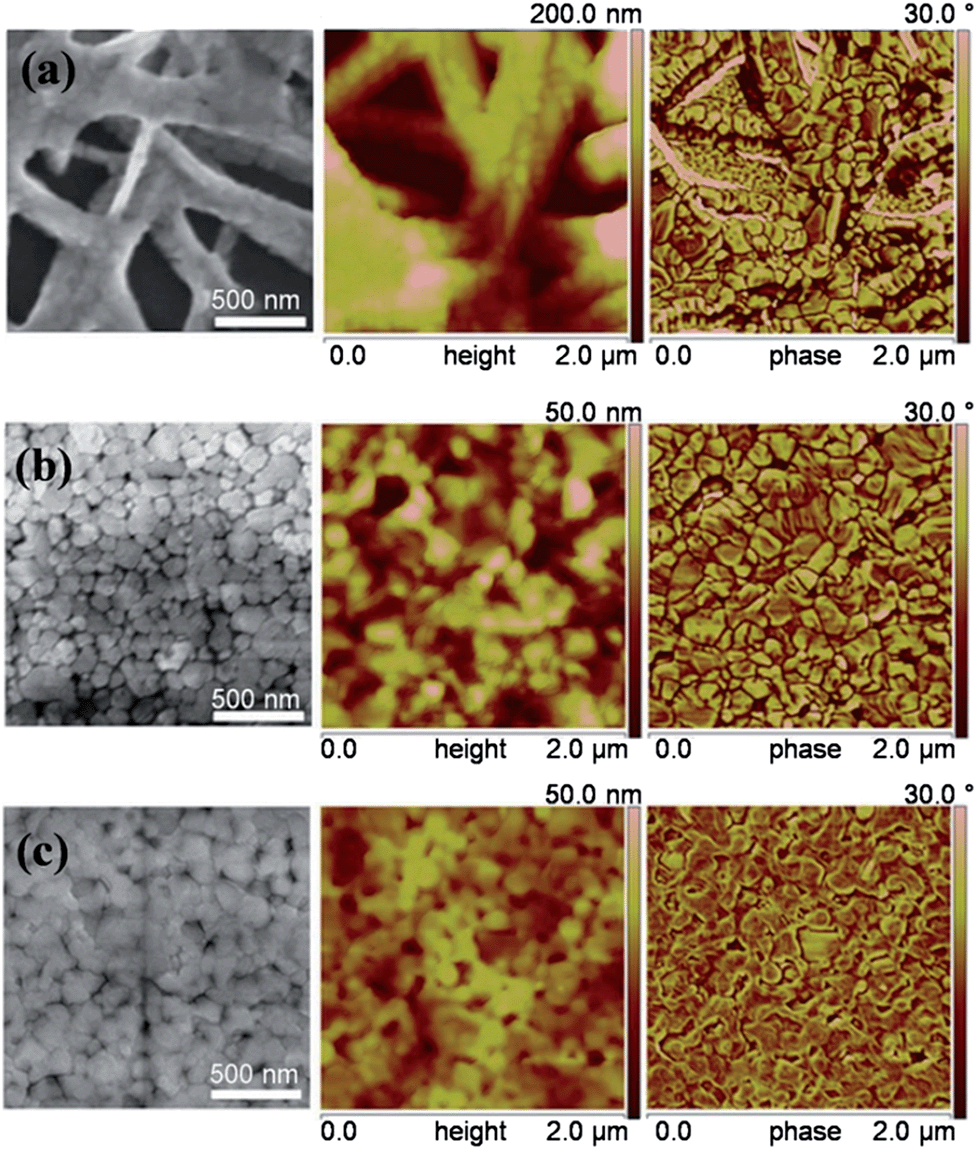 | ||
| Fig. 3 SEM (left), AFM height (middle) and phase (right) images for CH3NH3PbI3 films fabricated using no additive (a), 17.5 mg mL−1 CH3NH3Cl (b), and 17.5 mg mL−1 NH4Cl (c), respectively. | ||
Solar cells with structure ITO/PEDOT:PSS/CH3NH3PbI3/PC61BM/Al were fabricated to investigate the effect of additives on photovoltaic performance. Device performance data are listed in Table 1. The device fabricated using no additive exhibited an open-circuit voltage (Voc) of 0.37 V, a short-circuit current density (Jsc) of 0.36 mA cm−2, a fill factor of 27.53% and a power conversion efficiency (PCE) of 0.04% (Fig. 4). The performance of the device fabricated using no additive being inconsistent with previous reports13,16 is due to the thickness difference between CH3NH3PbI3 films. The CH3NH3PbI3 film fabricated in this work using no additive is thicker (ca. 150 nm), and the imperfect crystallinity and morphology lead to poor device performance. Thick CH3NH3PbI3 films with high crystallinity and good morphology are obtained by using additives, and they give higher Jsc than previous films.13,16 The optimization data for device performance are listed in Tables S1–S5.† The optimized concentrations of CH3NH3Cl and NH4Cl additives are 20.0 mg mL−1 and 17.5 mg mL−1, respectively. The device fabricated using the CH3NH3Cl additive gave a Voc of 0.92 V, a Jsc of 12.78 mA cm−2, a FF of 69.40% and a PCE of 8.16%. The device fabricated using the NH4Cl additive gave a Voc of 0.88 V, a Jsc of 14.08 mA cm−2, a FF of 80.11% and a PCE of 9.93%. Higher Jsc and FF of devices fabricated using the NH4Cl additive result from a highly crystalline, more uniform and smoother CH3NH3PbI3 film. The thickness of the PC61BM layer was optimized (Table S3†). A 32 nm PC61BM layer gave the best performance. A thinner PC61BM layer can reduce the series resistance (Rs) of devices, leading to higher FF. The FF decreased when further reducing the thickness of the PC61BM layer, which resulted from the decrease of the shunt resistance. The solar cells fabricated using additives showed high reproducibility, which benefits from high crystallinity and good morphology of the CH3NH3PbI3 film. The integrated photocurrent for the devices fabricated using CH3NH3Cl and NH4Cl additives is 12.26 mA cm−2 and 13.32 mA cm−2, respectively, which is consistent with Jsc values obtained from J–V measurements. The mechanism how NH4Cl makes the perovskite film smooth is not clear, possibly related to crystallization kinetics. NH4Cl could slow down the crystallization process to make perfect perovskite crystals. Good crystallinity and morphology for the perovskite layer favor exciton generation and charge carrier transport. Also, using a high-quality perovskite film, the above electron-transport layer can be made thinner to reduce the series resistance.
 | ||
| Fig. 4 J–V curves (a) and EQE spectra (b) for CH3NH3PbI3 solar cells fabricated by using different additives. | ||
In summary, an innovative approach by using the chloride additive to enhance the performance of perovskite solar cells was developed. The effects of two additives CH3NH3Cl and NH4Cl on perovskite film properties and photovoltaic performance were investigated. Perovskite films fabricated using the NH4Cl additive are highly crystalline and possess excellent morphology, leading to remarkable enhancement in the device performance. CH3NH3PbI3/PC61BM solar cells fabricated using the NH4Cl additive gave a decent PCE of 9.93% and a very outstanding FF of 80.11%. Application of this innovative approach in other device structures is ongoing in our lab.
Acknowledgements
This work was supported by the “100 Talents Program” of Chinese Academy of Sciences and National Natural Science Foundation of China (21374025).Notes and references
- M. M. Lee, J. Teuscher, T. Miyasaka, T. N. Murakami and H. J. Snaith, Science, 2012, 338, 643 CrossRef CAS PubMed.
- H.-S. Kim, C.-R. Lee, J.-H. Im, K.-B. Lee, T. Moehl, A. Marchioro, S.-J. Moon, R. Humphry-Baker, J.-H. Yum, J. E. Moser, M. Grätzel and N.-G. Park, Sci. Rep., 2012, 2, 1 Search PubMed.
- J. Burschka, N. Pellet, S.-J. Moon, R. Humphry-Baker, P. Gao, M. K. Nazeeruddin and M. Grätzel, Nature, 2013, 499, 316 CrossRef CAS PubMed.
- M. Liu, M. B. Johnston and H. J. Snaith, Nature, 2013, 501, 395 CrossRef CAS PubMed.
- A. Kojima, K. Teshima, Y. Shirai and T. Miyasaka, J. Am. Chem. Soc., 2009, 131, 6050 CrossRef CAS PubMed.
- J.-H. Im, C.-R. Lee, J.-W. Lee, S.-W. Park and N.-G. Park, Nanoscale, 2011, 3, 4088 RSC.
- K. Wojciechowski, M. Saliba, T. Leijtens, A. Abate and H. J. Snaith, Energy Environ. Sci., 2014, 7, 1142 CAS.
- S. Kazim, M. K. Nazeeruddin, M. Grätzel and S. Ahmad, Angew. Chem., Int. Ed., 2014, 53, 2812 CrossRef CAS PubMed.
- S. D. Stranks, G. E. Eperon, G. Grancini, C. Menelaou, M. J. P. Alcocer, T. Leijtens, L. M. Herz, A. Petrozza and H. J. Snaith, Science, 2013, 342, 341 CrossRef CAS PubMed.
- J. H. Heo, S. H. Im, J. H. Noh, T. N. Mandal, C.-S. Lim, J. A. Chang, Y. H. Lee, H.-J. Kim, A. Sarkar, M. K. Nazeeruddin, M. Grätzel and S. I. Seok, Nat. Photonics, 2013, 7, 486 CrossRef CAS.
- C. Roldán-Carmona, O. Malinkiewicz, A. Soriano, G. M. Espallargas, A. Garcia, P. Reinecke, T. Kroyer, M. I. Dar, M. K. Nazeeruddin and H. J. Bolink, Energy Environ. Sci., 2014, 7, 994 Search PubMed.
- J.-Y. Jeng, Y.-F. Chiang, M.-H. Lee, S.-R. Peng, T.-F. Guo, P. Chen and T.-C. Wen, Adv. Mater., 2013, 25, 3727 CrossRef CAS PubMed.
- S. Sun, T. Salim, N. Mathews, M. Duchamp, C. Boothroyd, G. Xing, T. C. Sum and Y. M. Lam, Energy Environ. Sci., 2014, 7, 399 CAS.
- P. Docampo, J. M. Ball, M. Darwich, G. E. Eperon and H. J. Snaith, Nat. Commun., 2013, 4, 2761 Search PubMed.
- O. Malinkiewicz, A. Yella, Y. H. Lee, G. M. Espallargas, M. Grätzel, M. K. Nazeeruddin and H. J. Bolink, Nat. Photonics, 2014, 8, 128 CrossRef CAS.
- H.-B. Kim, H. Choi, J. Jeong, S. Kim, B. Walker, S. Song and J. Y. Kim, Nanoscale, 2014, 6, 6679 RSC.
- G. E. Eperon, V. M. Burlakov, P. Docampo, A. Goriely and H. J. Snaith, Adv. Funct. Mater., 2014, 24, 151 CrossRef CAS.
- G. Xing, N. Mathews, S. Sun, S. S. Lim, Y. M. Lam, M. Grätzel, S. Mhaisalkar and T. C. Sum, Science, 2013, 342, 344 CrossRef CAS PubMed.
- Q. Wang, Q. Dong, Z. Xiao, Y. Yuan and J. Huang, Energy Environ. Sci., 2014, 7, 2359 CAS.
Footnote |
| † Electronic supplementary information (ESI) available: Experimental details, measurements and instruments. See DOI: 10.1039/c4nr02425g |
| This journal is © The Royal Society of Chemistry 2014 |