 Open Access Article
Creative Commons Attribution 3.0 Unported Licence
Single crystalline wurtzite ZnO/zinc blende ZnS coaxial heterojunctions and hollow zinc blende ZnS nanotubes: synthesis, structural characterization and optical properties†
Xing
Huang
ab,
Marc-Georg
Willinger
b,
Hua
Fan
a,
Zai-lai
Xie
b,
Lei
Wang
a,
Achim
Klein-Hoffmann
b,
Frank
Girgsdies
b,
Chun-Sing
Lee
c and
Xiang-Min
Meng
*a
aKey Laboratory of Photochemical Conversion and Optoelectronic Materials, Technical Institute of Physics and Chemistry, Chinese Academy of Sciences, Beijing, 100190, P. R. China. E-mail: mengxiangmin@mail.ipc.ac.cn
bDepartment of Inorganic Chemistry, Fritz Haber Institute of the Max Planck Society, Faradayweg 4-6, 14195 Berlin, Germany
cCenter of Super-Diamond and Advanced Films (COSDAF) & Department of Physics and Materials Science, City University of Hong Kong, Hong Kong SAR, P. R. China
First published on 23rd May 2014
Abstract
Synthesis of ZnO/ZnS heterostructures under thermodynamic conditions generally results in the wurtzite (WZ) structure of the ZnS component because its WZ phase is thermodynamically more stable than its zinc blende (ZB) phase. In this report, we demonstrate for the first time the preparation of ZnO/ZnS coaxial nanocables composed of single crystalline ZB structured ZnS epitaxially grown on WZ ZnO via a two-step thermal evaporation method. The deposition temperature is believed to play a crucial role in determining the crystalline phase of ZnS. Through a systematic structural analysis, the ZnO core and the ZnS shell are found to have an orientation relationship of (0002)ZnOWZ//(002)ZnSZB and [01−10]ZnOWZ//[2−20]ZnSZB. Observation of the coaxial nanocables in cross-section reveals the formation of voids between the ZnO core and the ZnS shell during the coating process, which is probably associated with the nanoscale Kirkendall effect known to result in porosity. Furthermore, by immersing the ZnO/ZnS nanocable heterojunctions in an acetic acid solution to etch away the inner ZnO cores, single crystalline ZnS nanotubes orientated along the [001] direction of the ZB structure were also achieved for the first time. Finally, optical properties of the hollow ZnS tubes were investigated and discussed in detail. We believe that our study could provide some insights into the controlled fabrication of one dimensional (1D) semiconductors with desired morphology, structure and composition at the nanoscale, and the synthesized WZ ZnO/ZB ZnS nanocables as well as ZB ZnS nanotubes could be ideal candidates for the study of optoelectronics based on II–VI semiconductors.
Introduction
Semiconductors with geometric, structural and compositional modulation at the nanoscale remain very attractive objects in nanoscience and nanotechnology.1–5 With numerous efforts devoted in the past two decades, 1D semiconductors with various geometries including nanowires,6 nanoribbons,7 nanotubes,8 and nanocombs,9etc, have been successfully synthesized and incorporated in devices demonstrating their potential for electronic, photonic, catalytic, and energy-related applications.10–14 Whilst earlier studies concentrated mainly on the synthesis and characterization of single-phase semiconductors,15–19 recent research has been oriented toward the preparation of 1D hetero-semiconductors aiming to achieve superior performances by taking advantage of integrated multifunctionality of the disparate components.20–23 So far, various functional 1D hetero-semiconductors have been achieved via physical and chemical processes such as Si/Ge axial nanowires,24 GaN/ZnS core/shell nanorods,25 CdS/Ag2S superlattice,26 ZnO/ZnS biaxial nanoribbon,27etc. In particular, heterogenous ZnO/ZnS nanostructures are of great interest to researchers not only for their potential application as UV sensors,28,29 but also due to their considerable value for fundamental research in a variety of aspects such as bandgap transition,30 charge transfer,31 anion exchange,32 electricity generation33 and so forth. Many cases of intriguing and unique phenomena exposed through the combination of ZnO and ZnS to form 1D ZnO/ZnS heterostructures have further deepened our understanding of the resulting heteromaterials at the nanoscale. As one of the long term challenges in this field, the synthesis of 1D ZnO/ZnS heterostructures in a controllable manner over the morphology, structure, and orientation of the constituted ZnO and ZnS is awaiting to be overcome.Previously, we have realized a controlled fabrication of single crystalline ZnO/ZnS nanocable heterostructures with the inner ZnO core and outer ZnS shell holding the same crystallographic structure (WZ structure) and orientation ((0001)ZnOWZ//(0001)ZnSWZ and [01−10]ZnOWZ//[01−10]ZnSWZ).34 In addition, several other forms of 1D ZnO/ZnS heterostructures including ZnO/ZnS biaxial nanoribbons,27 ZnO/ZnS rings35 and ZnO/ZnS axial nanowires33 have also been achieved elsewhere through a thermal vaporizing process in the past few years. One common characteristic of those aforementioned ZnO/ZnS heterostructures is that the ZnS component shows a WZ structure rather than a ZB structure because its WZ phase is more favorable over its ZB phase under thermodynamic conditions. Structural differences between the two polymorphs can be described by the sequence of atomic layers stacking parallel to {111} of ZB or {0001} of WZ planes in terms of the ABCABC or ABABAB pattern35 (atomic models of the WZ and the ZB ZnS are shown in Fig. S1†). Although the difference in the atomic arrangement is subtle, it causes a large difference in the physical properties. Considering their electronic structures for example, ZB ZnS has a band-gap of 3.72 eV, whereas the band-gap of WZ ZnS is 3.77 eV.36
On the other hand, although ZnO/ZnS heterostructures with ZnS possessing a ZB phase can be synthesized through solution processes at relatively low temperatures, the ZnS component is usually polycrystalline and does not show any orientation relationship with the ZnO host.37,38 For the development of high performance optoelectronic nanodevices based on 1D hetero-semiconductors, candidates with the single crystalline feature as well as controlled structures and orientations are highly desirable.28,39
In this work, we introduce a new type of ZnO/ZnS coaxial heterostructure. The heterostructure was synthesized by a two-step thermal evaporation process, which led to the growth of single crystalline ZB ZnS on the ZnO nanorod. Through detailed electron microscopic studies of the heterojunction, we were able to identify an epitaxial relationship of (0002)ZnOWZ//(002)ZnSZB and [01−10]ZnOWZ//[2−20]ZnSZB. In addition, from cross-sections of these heterostructures, voids were observed between the ZnO core and the ZnS shell, which are believed to be resulting from the nanoscale Kirkendall effect.40 After simple solution treatment to etch away the inner ZnO cores, hexagonal shaped single crystalline ZnS nanotubes orientated along the [002] direction of the ZB structure were also obtained for the first time. The as-prepared single crystalline ZnO/ZnS nanocables and relevant hollow ZnS tubes could be promising materials for optoelectronic applications.
Experimental
Synthesis of ZnO/ZnS core/shell nanorods
The ZnO/ZnS core/shell nanorods were fabricated by a two-step thermal evaporation process. Firstly, we synthesized the ZnO nanorods on a silicon wafer by heating the Zn source in the presence of oxygen similar to our previous work. Next, we placed the ZnS powder at the high-temperature zone of the quartz tube and the obtained ZnO nanorods at the low-temperature zone. After the pressure in the tube was pumped down to 0.1 Pa, high-purity argon mixed with 5% hydrogen was introduced into the tube at a constant rate of 50 sccm. Deposition was carried out by heating the ZnS to 700 °C and the ZnO nanorods to 550 °C. The pressure in the system was kept at about 600 Pa during the experiment. After the deposition process, the furnace was naturally cooled down to room temperature.Preparation of ZnS nanotubes
We put the ZnO/ZnS core/shell nanorods in an acetic acid solution (20 wt%) for three hours to remove the inner ZnO cores and then dried them in air at room temperature.Preparation of cross-section of ZnO/ZnS core/shell nanorods
Firstly, we had the core/shell nanorods embedded in epoxy and glued between two slices of Si wafers. This sandwich was then thinned from both sides with SiC grinding paper and diamond lapping film up to about 10 microns in thickness. After gluing on an aperture hole, the TEM cross-section sample was prepared by ion beam etching in a PIPS (Precision Ion Polishing System) 619 system from both sides up to the electron transparency.Preparation of cross-section of ZnS nanotubes
The ZnS nanotubes were firstly embedded in epoxy plastic which was then cut into slices with a thickness of about 50 nm by using a PowerTome Ultramicrotome. Finally, the slices were transferred onto a TEM grid.Characterization
SEM images of the samples were taken with Hitachi S-4300 and S-4800 scanning electron microscopes. TEM and HRTEM images were recorded using JEM-2100F and FEI Cs-corrected Titan 80–300 microscopes. X-ray diffraction patterns of the samples were recorded on a Bruker D8 Advance powder X-ray diffractometer. Cathodoluminescence spectra were collected on a Quanta 200F SEM operated at 15 kV.Results and discussion
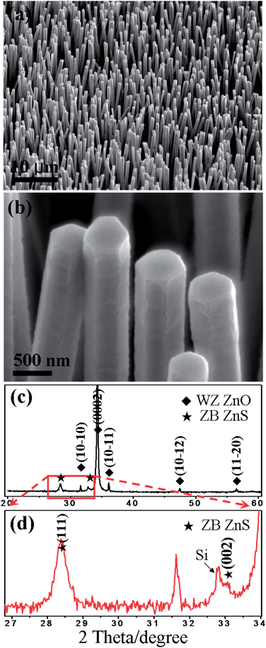
The experimental set-up (a high temperature furnace with two heating zones) and processing strategy (from arrays of ZnO nanorods to arrays of ZnS nanotubes) of this work are schematically illustrated in Fig. 1a and b. Firstly, arrays of ZnO nanorods were synthesized using Zn powder in the presence of oxygen via a thermal deposition method as reported in our previous work.41 Scanning electron microscopy (SEM) analysis demonstrates that the as-prepared ZnO nanorods have a length of about 30 micrometers and diameters ranging from 200 to 400 nanometers (Fig. S2†). Owing to its WZ structure, the ZnO nanorods have hexagonal cross-sections. Transmission electron microscopy (TEM) investigation further reveals that the ZnO nanorods are preferentially orientated along the [0001] direction. The ZnO nanorod array was then used as a template for further deposition of a ZnS layer on it via thermal deposition (Fig. 1a). Morphological analysis shows that the products obtained (Fig. 2a and b) become significantly larger in diameter in comparison to bare ZnO nanorods. Close observation confirms that a thin layer, uniformly and compactly covering the surfaces of ZnO nanorods, has been formed. In some cases, the nanolayers show cracks along the edges of the nanorods, as indicated in Fig. 2b. X-ray diffraction (XRD) measurement was performed to investigate the phase structure of the products (Fig. 2c). Due to the c-axis orientation, the ZnO nanorods within nanocables exhibit a strong reflection located at around 34.5°, corresponding to the (0002) planes of WZ structured ZnO (JPCDS, No. 36-1451). Besides, several relatively weak peaks originating from ZnO rods can be observed as well, as indexed in the image. In addition to those reflections from ZnO, three additional peaks were clearly identifiable (Fig. 2d): one at around 32.8° is believed to come from the (002) reflection of the Si substrate and the other two located at about 28.5° and 33.1° respectively can be rationally indexed to the (111) and (002) planes of ZB ZnS (JCPDS, No. 05-0566).36 Based on the current evidence, therefore, the formation of ZnO/ZnS heterojunctions within the shell of ZnS holding a ZB structure is primarily demonstrated.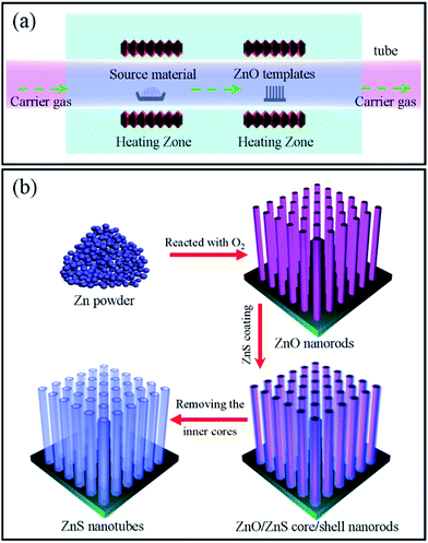 | ||
| Fig. 1 (a) Schematic diagram of a high temperature furnace with two heating zones. (b) Fabrication strategies from arrays of ZnO nanorods to arrays of the hollow ZnS nanotubes. | ||
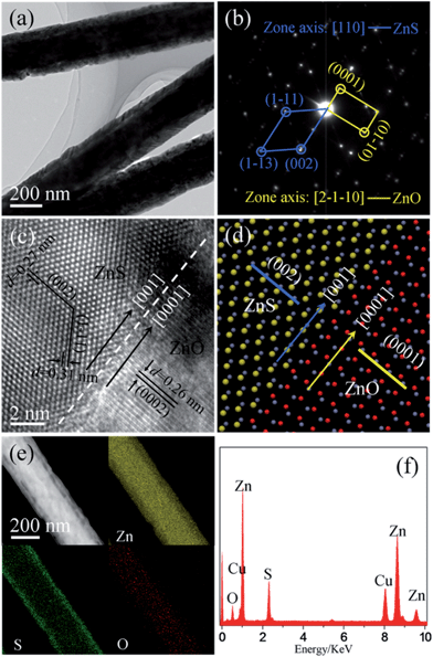
In order to understand the crystal structure of the ZnS nanolayer further, TEM and selected area electron diffraction (SAED) were employed. Fig. 3a shows a low-magnification TEM image of the ZnO/ZnS nanorods. The dark/bright contrast along the radial direction of the nanorods indicates that ZnO nanorods have been fully covered with a layer of ZnS, which measures around 50 nm in thickness. Fig. 3b displays the corresponding SAED pattern of the heterojunction. Two sets of diffraction spots are shown in the image, which can be indexed respectively to the [2−1−10] zone axis pattern of the WZ ZnO and the [110] zone axis pattern of the ZB ZnS.
Fig. 3c shows a high-resolution TEM (HRTEM) image recorded from the interface region of the heterojunction. The marked d-spacings of 0.31 and 0.27 nm in the shell area correspond to those of (1−11) and (002) lattice fringes of ZB ZnS, while the interplanar distance of 0.26 nm labeled in the core region matches well with that of the (0002) plane of WZ ZnO. An epitaxial orientation relationship between the inner WZ ZnO core and the ZB ZnS shell can be concluded according to the above structural analysis: (0002)ZnOWZ//(002)ZnSZB and [2−1−10]ZnOWZ//[110]ZnSZB, as schematically illustrated in Fig. 3d. In addition, composition analysis of the resulting heterostructures was carried out using energy-dispersive X-ray spectrometry (EDX) and elemental mapping in dark-field (DF) scanning TEM (STEM) mode. As can be seen from Fig. 3e, oxygen is only distributed within the core region while the sulfur signal is confined exclusively in the shell area. The signal from Zn can be detected throughout the entire nanorod. Combined with the EDX data shown in Fig. 3f, the core/shell construction of the ZnO/ZnS heterojunctions with a ZB structured ZnS shell is confirmed.
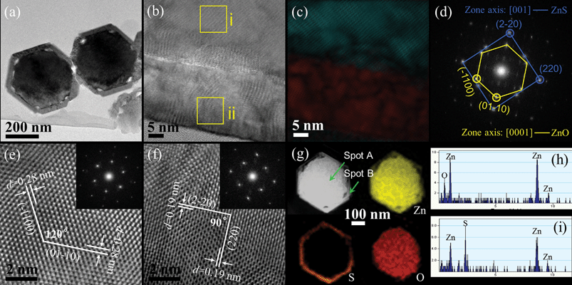
To further verify the intrinsic crystal structure and the orientation relationship in detail from an axial view of the nanocables, cross-sectional samples were prepared as displayed in Fig. 4a. Images of the cross-section show that the ZnO core is completely covered by the hexagonal ZnS shell with a uniform thickness of about 40 nm, consistent with the former observation shown in Fig. 3a. It is noteworthy that there are some voids at the ZnO/ZnS interface, particularly near corners of the hexagonal ZnO core (Fig. S3†). This phenomenon is analogous to the Kirkendall effect known to result in porosity due to the difference in diffusion rates between two components in a diffusion couple.40,42 It has been demonstrated by Alivisatos' group that anion exchange reaction accompanied by the nanoscale Kirkendall effect in the binary ZnO would yield ZnO/ZnS yolk–shell nanoparticles with nanopores in between through solution treatment. The faster diffusion speed of O2− compared to that of the incoming S2− leads to the formation of a porous structure.32 In the present case, the growth of the ZnS layer on the ZnO surface would introduce a highly strained interface between the ZnO core and the ZnS shell due to the large lattice mismatch. To relax this strain energy, the corners of ZnO, considered to possess more strain energy density, would primarily diffuse into the ZnS shell through the center bridges of the interface by the anion exchange reaction (Fig. S4†). Alternatively, the absence of corners could simply be due to thermal evaporation of ZnO at the corners during the coating process. To examine this supposition, we carried out an in situ experiment by only heating the ZnO nanorods at 550 °C for two hours in the presence of Ar![[thin space (1/6-em)]](https://www.rsc.org/images/entities/char_2009.gif) :
:![[thin space (1/6-em)]](https://www.rsc.org/images/entities/char_2009.gif) H2 (95%
H2 (95%![[thin space (1/6-em)]](https://www.rsc.org/images/entities/char_2009.gif) :
:![[thin space (1/6-em)]](https://www.rsc.org/images/entities/char_2009.gif) 5%) gas. The result is shown in Fig. S5.† Although some valley structures were observed on the top surface, the ZnO nanorods after heating do not show much difference in the shape compared to the original ones. Therefore, to some extent, this evidence makes the nanoscale Kirkendall effect more reasonable for the vanishing of corners of ZnO upon forming the ZnS shell. Fig. 4b and c show an HRTEM image and its corresponding RGB image of the core/shell nanorod, respectively. The differences in contrast and colors in the images unveil the differences in composition and structure of the core and shell areas. Fig. 4d presents a Fast Fourier transform (FFT) of the lattice fringes in Fig. 4b in which two sets of diffraction spots that respectively correspond to WZ ZnO and ZB ZnS are observed. The zone axes for ZnO and ZnS can be indexed to [0001] of the WZ structure and [001] of the ZB structure, meaning that the exposed crystal planes of the ZnO core and the ZnS shell correspond to the (0002) planes for WZ ZnO and the (002) planes for ZB ZnS. An epitaxial orientation relationship between the inner ZnO core and the ZnS shell is therefore identified as: (0002)ZnOWZ//(002)ZnSZB and [01−10]ZnOWZ//[2−20]ZnSZB. Structurally, this result agrees well with the previous analysis shown in Fig. 3. Fig. 4e and f, respectively, depict the enlarged HRTEM images of the core/shell nanorod taken from the areas i and ii in Fig. 4b. The lattice fringes of WZ ZnO (01−10) and ZB ZnS (2–20) with d-spacings of 0.28 nm (Fig. 4e) and 0.19 nm (Fig. 4f) are revealed. To confirm the composition of the core/shell architecture of the sample, a detailed composition analysis was also conducted using the STEM elemental mapping. From the images exhibited in Fig. 4g–i, it is quite clear that the core region is bare ZnO and the hexagonal shell is ZnS.
5%) gas. The result is shown in Fig. S5.† Although some valley structures were observed on the top surface, the ZnO nanorods after heating do not show much difference in the shape compared to the original ones. Therefore, to some extent, this evidence makes the nanoscale Kirkendall effect more reasonable for the vanishing of corners of ZnO upon forming the ZnS shell. Fig. 4b and c show an HRTEM image and its corresponding RGB image of the core/shell nanorod, respectively. The differences in contrast and colors in the images unveil the differences in composition and structure of the core and shell areas. Fig. 4d presents a Fast Fourier transform (FFT) of the lattice fringes in Fig. 4b in which two sets of diffraction spots that respectively correspond to WZ ZnO and ZB ZnS are observed. The zone axes for ZnO and ZnS can be indexed to [0001] of the WZ structure and [001] of the ZB structure, meaning that the exposed crystal planes of the ZnO core and the ZnS shell correspond to the (0002) planes for WZ ZnO and the (002) planes for ZB ZnS. An epitaxial orientation relationship between the inner ZnO core and the ZnS shell is therefore identified as: (0002)ZnOWZ//(002)ZnSZB and [01−10]ZnOWZ//[2−20]ZnSZB. Structurally, this result agrees well with the previous analysis shown in Fig. 3. Fig. 4e and f, respectively, depict the enlarged HRTEM images of the core/shell nanorod taken from the areas i and ii in Fig. 4b. The lattice fringes of WZ ZnO (01−10) and ZB ZnS (2–20) with d-spacings of 0.28 nm (Fig. 4e) and 0.19 nm (Fig. 4f) are revealed. To confirm the composition of the core/shell architecture of the sample, a detailed composition analysis was also conducted using the STEM elemental mapping. From the images exhibited in Fig. 4g–i, it is quite clear that the core region is bare ZnO and the hexagonal shell is ZnS.
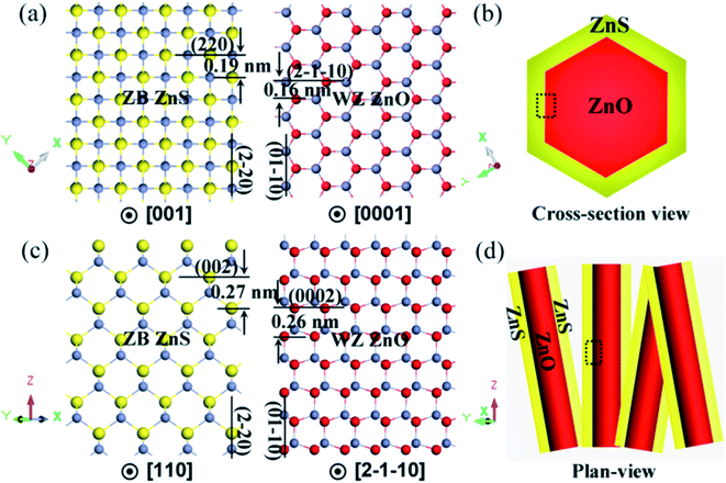
As stated in the Introduction, we have fabricated a type of single crystalline ZnO/ZnS core/shell nanorod with a ZnS shell in the WZ structure previously. The ZnS shell retains the same crystal structure and orientation as the inner ZnO core with an epitaxial relationship of (01−10)ZnO//(01−10)ZnS and [0001]ZnO//[0001]ZnS.34 In this work, the ZnS shell of the ZnO/ZnS nanocables is obtained in the ZB phase instead of the WZ phase. Structural analysis revealed that the present core/shell nanorods were formed via an epitaxial growth of ZnS ZB {2−20} planes on the {01−10} planes of WZ ZnO. Note that ZB ZnS (a = 0.5406 nm) and WZ ZnO (a = b = 0.3249 nm, c = 0.5206 nm) belong to different structural systems, and therefore the lattice mismatches between the different epitaxial planes are diverse. Shown in Fig. 5a are atomic models of the ZB ZnS(002) plane and the WZ ZnO(0002) plane, respectively. The d-spacings for ZB ZnS(220) and WZ ZnO(2−1−10) planes are 0.19 nm and 0.16 nm, as labeled in the image. The lattice mismatch between the ZnS(220) plane and the ZnO(2−1−10) plane is 18.7% with reference to ZnO. For another pair of epitaxial planes, i.e., ZnS(002) and ZnO(0002) with d-spacings of 0.27 nm and 0.26 nm (see Fig. 5c and d), their lattice mismatch is much lower, which is 3.8%. The structural incompatibility and large lattice mismatches between ZB ZnS and WZ ZnO tend to result in polycrystalline ZnS nanoparticles on the ZnO surface without any crystal orientation relationship as reported elsewhere.37 To the best of our knowledge, the formation of epitaxial WZ ZnO/ZB ZnS core/shell heterojunctions with the ZnS shell holding the single crystalline nature has not been achieved until now.
The growth mechanism of the coaxial core/shell nanorods is discussed in the following on the basis of the above structural analysis. Due to the absence of metal catalysts such as Au or Ag, the growth of ZnO nanorod templates in the first step can be rationally explained by a self-catalyzed Vapor–Liquid–Solid (VLS) model.43 In this process, melted Zn/ZnOx liquid acts as the catalyst that continuously absorbs the surrounding ZnOx (0 < x ≤ 1) vapor for the growth of ZnO nanorods along the [0001] direction. This oxidation reaction can be simply described as: Zn/ZnOx(l) + O2(g) → ZnO(s). In the second step, the ZnS powder located at the high temperature zone is evaporated with the assistance of H2 to form Zn and H2S vapor through the following reaction: ZnS(s) + H2(g) → Zn(g) + H2S(g).44 The generated vapors are transported downstream by the carrier gas and nucleate on the ZnO surface to grow a layer of ZB ZnS. The achievement of ZnS with a ZB structure rather than the thermodynamically stable WZ ZnS phase here may be associated with the relatively low temperature of the deposition area in the system. In our previous work, we synthesized ZB-phased ZnS nanowires through a hydrogen-assisted thermal evaporation method by maintaining the deposition temperature at around 600 °C.45 It is known that the ZB structure has a lower bulk cohesive energy than the WZ structure, thus, at the low deposition temperature (550 °C) performed in the dynamic process, the growth of ZB ZnS instead of WZ ZnS may be energetically favorable. Besides, the lattice mismatch between ZB ZnS and WZ ZnO is smaller compared with that between WZ ZnS and WZ ZnO. This should be taken into consideration and could play a role in the formation of WZ ZnO/ZB ZnS coaxial heterostructures at low temperatures. It is worth mentioning that the synthesis of these nanomaterials is relatively sensitive to the experimental parameters such as reaction temperature, pressure, vapor dynamics and so forth.27,46,47 Different morphologies and structures have been observed due to the slight alteration of the environments.48,49 Obviously, more studies are needed to correlate the experimental conditions with the final structures in order to fulfill the controlled fabrication of nanomaterials. Nevertheless, our study here demonstrates the possibility of heteroepitaxial growth of the single crystalline ZB ZnS shell on the WZ ZnO core through a thermal deposition process.
Hollow nanostructures such as nano-spheres and nano-tubes with unique geometry and high surface-volume ratio have drawn both theoretical50–52 and experimental interest with respect to their great potential for applications in drug delivery,53 photocatalysis,54 photodetection,55 solar cells,56 Li-ion batteries,57 and so forth. Enlightened by those merits, we converted the ZnO/ZnS core/shell nanocables into hollow ZnS nanotubes by removing the inner ZnO cores through simple acetic acid solution treatment. Exhibited in Fig. 6a–f are several SEM images of the obtained ZnS nanotubes with a typical diameter of about 300 nm and a length of 30 micrometers (Fig. 6b and e). In solution processing, tips of the nanotubes stick together due to the capillary effect upon drying (Fig. 6a). Note that some of the tubes are broken along the cross-sections as marked with arrows (Fig. 6f), signifying the hollow structure of the ZnS nanotubes. XRD measurement was also carried out to confirm the structure of the tubes (Fig. S6†). Four peaks located at around 28.5°, 33.1°, 47.5°, and 56.4° are observed in the XRD pattern, in good accordance with the (111), (200), (220), and (311) lattice planes of ZB ZnS.
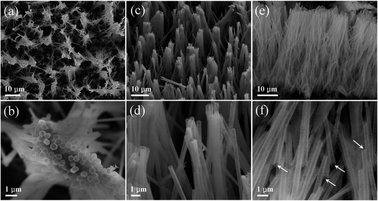 | ||
| Fig. 6 Low magnification (a) top-view, (c) tilt-view, and (e) plan-view SEM images of the ZnS nanotubes array; (b, d and f) enlarged SEM images of ZnS nanotubes corresponding to (a, c and e). | ||
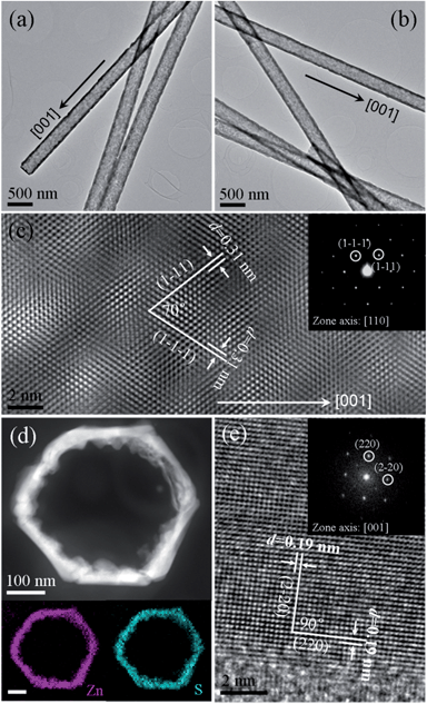
Fig. 7a and b are low-magnification plan-view TEM images of the obtained ZnS nanotubes with a wall thickness of around 40 nm. Although the thickness of the ZnS tube seems not homogenous, the HRTEM image and the SAED pattern (Fig. 7c) demonstrate that the ZnS tube is continuously single crystalline indeed and have a ZB structure orientated along the [001] direction. To get more detail about the composition and the intrinsic structure, cross-sections of the ZnS tubes were prepared. Shown in Fig. 7d is a DF-STEM image of the cross-sectional sample. The relevant EDX mapping clearly shows that the Zn and S elements are distributed homogeneously over the entire ring. It is noteworthy that the inner wall of the tube is quite rough (Fig. 7d), which could be further evidence for an ion exchange reaction occurring during the ZnS coating process. Fig. 7e shows the HRTEM image and FFT pattern of the ZnS ring. The interplanar distances of 0.19 nm match well with that of (2–20) and (220) planes of the ZB ZnS, consistent with our previous observation (Fig. 4b). The inset FFT pattern with a zone axis of [001] further confirms its single crystalline nature.
To determine the origin of the luminescence in the resulting nanomaterials, room temperature CL measurement was performed. Shown in Fig. 8a and b are the secondary electron (SE) image and the corresponding CL image of the resultant ZnS nanotubes, respectively. It can be clearly seen from images that a few ZnO cores remained inside the ZnS tubes on the top regions as marked with arrows in Fig. 8a. Comparison of the SE image and the CL image indicates that the regions with remaining ZnO cores (i.e. ZnO/ZnS core/shell heterostructures) give lower luminescence (dark contrast in Fig. 8b), while the pure ZnS tubes without the ZnO core show higher CL intensity (bright contrast in Fig. 8b). The low luminescence contribution from those ZnO/ZnS regions may be associated with the type-II band alignment of the ZnO/ZnS heterojunction28 (the schematic energy band diagram is shown in Fig. S7†). Owing to the internal field at the heterojunction interface, the electron–hole pairs generated under the illumination will be separated, i.e., electrons will move to the ZnO side while holes move to the ZnS side. This excitonic charge separation state would considerably decrease the recombination of the electron–hole pairs58,59 and result in weak luminescence of the ZnO/ZnS core/shell heterostructures. Fig. 8c shows a CL spectrum of the nanomaterial corresponding to the CL image in Fig. 8b. Two emission peaks located at 380 nm and 510 nm, respectively, were observed in the spectrum. Through correlating the CL image with the CL spectrum the origin of the luminescence can be figured out, that is, the weak emission peak at 380 nm can be ascribed to the bandgap emission of ZnO60 while the strong green emission at 510 nm is contributed by the ZnS tubes. Since no other impurity is found in this study, the green emission from the ZnS tubes may be derived from some self-activated centers, vacancy states, or interstitial states associated with the peculiar nanostructure.39,61 In addition, due to the large lattice mismatch between ZnO and ZnS, some structural defects such as misfit dislocations and stacking faults would probably exist in the ZnS layer (Fig. S8†), which may contribute partially to the observed green emission as well.
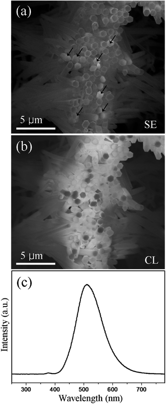 | ||
| Fig. 8 (a) SE image and (b) the corresponding CL image; (c) CL spectrum collected from the hollow ZnS tubes. | ||
Conclusions
In summary, our study demonstrates the possibility of growing a single crystalline ZB ZnS shell heteroepitaxially on a WZ ZnO core through a thermal deposition process. The orientation relationship between WZ ZnO and ZB ZnS is identified as (0002)ZnOWZ//(002)ZnSZB and [01−10]ZnOWZ//[2−20]ZnSZB by TEM. The anion exchange reaction of O2− with S2− accompanied by the nanoscale Kirkendall effect in the binary ZnO/ZnS interface leads to the formation of void spaces between the ZnO core and the ZnS shell. In addition, single crystalline ZnS nanotubes orientated along the [001] direction of the ZB structure can be obtained through selective etching of the inner ZnO cores. The CL measurement shows a strong green emission from the ZnS tubes, which may have originated from some self-activated centers, vacancy states, interstitial states or structural defects. However, due to the type-II band alignment of the ZnO/ZnS heterojunction that can efficiently decrease the recombination of the electron–hole pairs in both ZnO and ZnS, the ZnS tubes with residual ZnO on top regions show much lower emission intensity.Acknowledgements
We thank the financial support from the “Strategic Priority Research Program” of the Chinese Academy of Sciences (XDA09040203).Notes and references
- C. H. Cho, C. O. Aspetti, M. E. Turk, J. M. Kikkawa, S. W. Nam and R. Agarwal, Nat. Mater., 2011, 10, 669–675 CrossRef CAS PubMed.
- J. Xiang, W. Lu, Y. J. Hu, Y. Wu, H. Yan and C. M. Lieber, Nature, 2006, 441, 489–493 CrossRef CAS PubMed.
- L. Peng, L. Hu and X. Fang, Adv. Mater., 2013, 25, 5321–5328 CrossRef CAS PubMed.
- M. H. Huang, S. Mao, H. Feick, H. Q. Yan, Y. Y. Wu, H. Kind, E. Weber, R. Russo and P. D. Yang, Science, 2001, 292, 1897–1899 CrossRef CAS PubMed.
- X. Huang, M. Wang, L. D. Shao, M. G. Willinger, C. S. Lee and X. M. Meng, J. Phys. Chem. Lett., 2013, 4, 740–744 CrossRef CAS PubMed.
- J. W. Liu, J. Zheng, J. L. Wang, J. Xu, H. H. Li and S. H. Yu, Nano Lett., 2013, 13, 3589–3593 CrossRef PubMed.
- Z. T. Deng, D. Cao, J. He, S. Lin, S. M. Lindsay and Y. Liu, ACS Nano, 2012, 6, 6197–6207 CrossRef CAS PubMed.
- X. J. Xu, X. S. Fang, T. Y. Zhai, H. B. Zeng, B. D. Liu, X. Y. Hu, Y. Bando and D. Golberg, Small, 2011, 7, 445–449 CrossRef CAS PubMed.
- H. Q. Yan, R. R. He, J. Johnson, M. Law, R. J. Saykally and P. D. Yang, J. Am. Chem. Soc., 2003, 125, 4728–4729 CrossRef CAS PubMed.
- X. S. Fang, Y. Bando, C. H. Ye and D. Golberg, Chem. Commun., 2007, 3048–3050 RSC.
- Z. H. Lin, Y. N. Xie, Y. Yang, S. H. Wang, G. Zhu and Z. L. Wang, ACS Nano, 2013, 7, 4554–4560 CrossRef CAS PubMed.
- L. Shi, Y. M. Xu, S. K. Hark, Y. Liu, S. Wang, L. M. Peng, K. W. Wong and Q. Li, Nano Lett., 2007, 7, 3559–3563 CrossRef CAS.
- T. Dufaux, M. Burghard and K. Kern, Nano Lett., 2012, 12, 2705–2709 CrossRef CAS PubMed.
- Y. Shi, H. Y. Li, L. Wang, W. Shen and H. Z. Chen, ACS Appl. Mater. Interfaces, 2012, 4, 4800–4806 CAS.
- H. Yu and W. E. Buhro, Adv. Mater., 2003, 15, 416–419 CrossRef CAS.
- K. Q. Peng, Y. Xu, Y. Wu, Y. J. Yan, S. T. Lee and J. Zhu, Small, 2005, 1, 1062–1067 CrossRef CAS PubMed.
- C. J. Barrelet, Y. Wu, D. C. Bell and C. M. Lieber, J. Am. Chem. Soc., 2003, 125, 11498–11499 CrossRef CAS PubMed.
- Y. Jiang, X. M. Meng, J. Liu, Z. R. Hong, C. S. Lee and S. T. Lee, Adv. Mater., 2003, 15, 1195–1198 CrossRef CAS.
- J. Q. Hu, Y. Bando, Q. L. Liu and D. Golberg, Adv. Funct. Mater., 2003, 13, 493–496 CrossRef CAS.
- F. Zhang, Y. Ding, Y. Zhang, X. L. Zhang and Z. L. Wang, ACS Nano, 2012, 6, 9229–9236 CrossRef CAS PubMed.
- X. P. Qi, G. W. She, X. Huang, T. P. Zhang, H. M. Wang, L. X. Mu and W. S. Shi, Nanoscale, 2014, 6, 3182–3189 RSC.
- Y. Myung, D. M. Jang, T. K. Sung, Y. J. Sohn, G. B. Jung, Y. J. Cho, H. S. Kim and J. Park, ACS Nano, 2010, 4, 3789–3800 CrossRef CAS PubMed.
- H. L. Liu, G. W. She, X. Huang, X. P. Qi, L. X. Mu, X. M. Meng and W. S. Shi, J. Phys. Chem. C, 2013, 117, 2377–2381 CAS.
- C. Y. Wen, M. C. Reuter, J. Bruley, J. Tersoff, S. Kodambaka, E. A. Stach and F. M. Ross, Science, 2009, 326, 1247–1250 CrossRef CAS PubMed.
- L. F. Hu, M. M. Brewster, X. J. Xu, C. C. Tang, S. Gradecak and X. S. Fang, Nano Lett., 2013, 13, 1941–1947 CrossRef CAS PubMed.
- R. D. Robinson, B. Sadtler, D. O. Demchenko, C. K. Erdonmez, L. W. Wang and A. P. Alivisatos, Science, 2007, 317, 355–358 CrossRef CAS PubMed.
- X. Fan, M. L. Zhang, I. Shafiq, W. J. Zhang, C. S. Lee and S. T. Lee, Adv. Mater., 2009, 21, 2393–2396 CrossRef CAS.
- L. F. Hu, J. Yan, M. Y. Liao, H. J. Xiang, X. G. Gong, L. D. Zhang and X. S. Fang, Adv. Mater., 2012, 24, 2305–2309 CrossRef CAS PubMed.
- A. Bera and D. Basak, ACS Appl. Mater. Interfaces, 2010, 2, 408–412 CAS.
- J. Schrier, D. O. Demchenko and L. W. Wang, Nano Lett., 2007, 7, 2377–2382 CrossRef CAS PubMed.
- K. Wang, J. J. Chen, Z. M. Zeng, J. Tarr, W. L. Zhou, Y. Zhang, Y. F. Yan, C. S. Jiang, J. Pern and A. Mascarenhas, Appl. Phys. Lett., 2010, 96, 123105 CrossRef.
- J. Park, H. Zheng, Y. W. Jun and A. P. Alivisatos, J. Am. Chem. Soc., 2009, 131, 13943–13945 CrossRef CAS PubMed.
- M. Y. Lu, J. H. Song, M. P. Lu, C. Y. Lee, L. J. Chen and Z. L. Wang, ACS Nano, 2009, 3, 357–362 CrossRef CAS PubMed.
- X. Huang, M. Wang, M. G. Willinger, L. D. Shao, D. S. Su and X. M. Meng, ACS Nano, 2012, 6, 7333–7339 CrossRef CAS PubMed.
- X. Wu, P. Jiang, Y. Ding, W. Cai, S. S. Xie and Z. L. Wang, Adv. Mater., 2007, 19, 2319–2323 CrossRef CAS.
- X. S. Fang, T. Y. Zhai, U. K. Gautam, L. Li, L. M. Wu, B. Yoshio and D. Golberg, ZnS, Prog. Mater. Sci., 2011, 56, 175–287 CrossRef CAS.
- X. D. Wang, P. X. Gao, J. Li, C. J. Summers and Z. L. Wang, Adv. Mater., 2002, 14, 1732–1735 CrossRef CAS.
- R. Yi, G. Z. Qiu and X. H. Liu, J. Solid State Chem., 2009, 182, 2791–2795 CrossRef CAS.
- L. W. Yin, Y. Bando, J. H. Zhan, M. S. Li and D. Golberg, Adv. Mater., 2005, 17, 1972–1977 CrossRef CAS.
- Y. D. Yin, R. M. Rioux, C. K. Erdonmez, S. Hughes, G. A. Somorjai and A. P. Alivisatos, Science, 2004, 304, 711–714 CrossRef CAS PubMed.
- X. Huang, L. Shang, S. Chen, J. Xia, X. P. Qi, X. C. Wang, T. R. Zhang and X. M. Meng, Nanoscale, 2013, 5, 3828–3833 RSC.
- Y. D. Yin, C. K. Erdonmez, A. Cabot, S. Hughes and A. P. Alivisatos, Adv. Funct. Mater., 2006, 16, 1389–1399 CrossRef CAS.
- C. Y. Geng, Y. Jiang, Y. Yao, X. M. Meng, J. A. Zapien, C. S. Lee, Y. Lifshitz and S. T. Lee, Adv. Funct. Mater., 2004, 14, 589–594 CrossRef CAS.
- Y. Jiang, X. M. Meng, J. Liu, Z. Y. Xie, C. S. Lee and S. T. Lee, Adv. Mater., 2003, 15, 323–327 CrossRef CAS.
- X. M. Meng, J. Liu, Y. Jiang, W. W. Chen, C. S. Lee, I. Bello and S. T. Lee, Chem. Phys. Lett., 2003, 382, 434–438 CrossRef CAS.
- J. Yan, X. S. Fang, L. D. Zhang, Y. Bando, U. K. Gautam, B. Dierre, T. Sekiguchi and D. Golberg, Nano Lett., 2008, 8, 2794–2799 CrossRef CAS PubMed.
- G. Z. Shen, Y. Bando, B. D. Liu, D. Golberg and C. J. Lee, Adv. Funct. Mater., 2006, 16, 410–416 CrossRef CAS.
- N. S. Karan, S. Sarkar, D. D. Sarma, P. Kundu, N. Ravishankar and N. Pradhan, J. Am. Chem. Soc., 2011, 133, 1666–1669 CrossRef CAS PubMed.
- D. H. Fan, R. Zhang and X. H. Wang, Phys. E, 2010, 42, 2081–2085 CrossRef CAS.
- S. Pal, B. Goswami and P. Sarkar, J. Phys. Chem. C, 2007, 111, 1556–1559 CAS.
- S. Pal, B. Goswami and P. Sarkar, J. Phys. Chem. C, 2008, 112, 6307–6312 CAS.
- N. Krainara, J. Limtrakul, F. Illas and S. T. Bromley, J. Phys. Chem. C, 2013, 117, 22908–22914 CAS.
- Y. F. Zhu, T. Ikoma, N. Hanagata and S. Kaskel, Small, 2010, 6, 471–478 CrossRef CAS PubMed.
- N. K. Shrestha, J. M. Macak, F. Schmidt-Stein, R. Hahn, C. T. Mierke, B. Fabry and P. Schmuki, Angew. Chem., Int. Ed., 2009, 48, 969–972 CrossRef CAS PubMed.
- J. P. Zou, Q. Zhang, K. Huang and N. Marzari, J. Phys. Chem. C, 2010, 114, 10725–10729 CAS.
- A. B. F. Martinson, J. W. Elam, J. T. Hupp and M. J. Pellin, Nano Lett., 2007, 7, 2183–2187 CrossRef CAS PubMed.
- L. Hu and Q. W. Chen, Nanoscale, 2014, 6, 1236–1257 RSC.
- Z. Y. Zhang, C. L. Shao, X. H. Li, L. Zhang, H. M. Xue, C. H. Wang and Y. C. Liu, J. Phys. Chem. C, 2010, 114, 7920–7925 CAS.
- S. Saha, S. Sarkar, S. Pal and P. Sarkar, J. Phys. Chem. C, 2013, 117, 15890–15900 CAS.
- X. Huang, L. D. Shao, G. W. She, M. Wang, S. Chen and X. M. Meng, CrystEngComm, 2012, 14, 8330–8334 RSC.
- T. Y. Zhai, Z. J. Gu, H. B. Fu, Y. Ma and J. N. Yao, Cryst. Growth Des., 2007, 7, 1388–1392 CAS.
Footnote |
† Electronic supplementary information (ESI) available: A crystallographic unit cell and periodic structure model of WZ ZnS and ZB ZnS; SEM, TEM and HRTEM images of ZnO nanorods; a top view SEM image of the ZnO nanorod and a TEM image of the ZnO/ZnS core/shell cross-sections; SEM images of the ZnO nanorod before and after heating at 550 °C in an Ar![[thin space (1/6-em)]](https://www.rsc.org/images/entities/char_2009.gif) : :![[thin space (1/6-em)]](https://www.rsc.org/images/entities/char_2009.gif) H2 (95% H2 (95%![[thin space (1/6-em)]](https://www.rsc.org/images/entities/char_2009.gif) : :![[thin space (1/6-em)]](https://www.rsc.org/images/entities/char_2009.gif) 5%) atmosphere; XRD data of hollow ZnS nanotubes; a schematic energy band diagram of the ZnO/ZnS core/shell heterostructure under illumination; a HRTEM image of the ZnS shell showing the stalking faults. See DOI: 10.1039/c4nr01575d 5%) atmosphere; XRD data of hollow ZnS nanotubes; a schematic energy band diagram of the ZnO/ZnS core/shell heterostructure under illumination; a HRTEM image of the ZnS shell showing the stalking faults. See DOI: 10.1039/c4nr01575d |
| This journal is © The Royal Society of Chemistry 2014 |

