 Open Access Article
Harnessing catalysis to enhance scanning probe nanolithography
Stewart A. M.
Carnally
and
Lu Shin
Wong
*
Manchester Institute of Biotechnology, School of Chemistry, University of Manchester, Manchester M13 9PL, UK. E-mail: l.s.wong@manchester.ac.uk
First published on 27th March 2014
Abstract
The use of scanning probes bearing catalysts to perform surface nanolithography combines the exquisite spatial precision of scanning probe microscopy with the synthetic capabilities of (bio)chemical catalysis. The ability to use these probes to direct a variety of localised chemical reactions enables the generation of nanoscale features with a high degree of chemical complexity in a “direct-write” manner. This article surveys the range of reactions that have been employed and the key factors necessary for the successful use of such catalytic scanning probes. These factors include the experimental parameters such as write speed, force applied to the probes and temperature; as well as the processes involved in the preparation of the catalysts on the probes and the surface that is to be fabricated. Where possible, the various reactions are also compared and contrasted; and future perspectives are discussed.
1. Introduction
One of the key requirements in the development of nanotechnological devices for sensing, diagnostics and information storage is the need to generate nanometre-sized features on a variety of surfaces. In this respect, the application of scanning probe lithography methods related to atomic force microscopy (AFM) have been widely adopted for their nanoscopic resolution and registry. Within this family of nanofabrication techniques, the probe tip is employed to modify the chemistry of a surface in a spatially controlled manner.There have been many examples of physical manipulation of surfaces by the probe tip in order to generate nanoscale features.1 These include mechanical removal of material (nanoshaving2), which may be integrated with subsequent back-filling with a contrasting chemical species (nanografting3); the application of an electrical bias between the probe and the surface to induce electrochemical oxidation (local anodic oxidation4); and heating the probe to induce thermochemical reactions (thermochemical nanolithography5).
Scanning probes have also been used for the local deposition of materials by using the probe to deliver molecular ‘inks’ to the surface. The most well-known of these techniques is dip pen nanolithography (DPN) and its derivatives including polymer pen lithography (PPL) and hard-tip soft-spring lithography (HSL).6–8 Scanning probes with microfluidic channels such as ‘nanopipettes’9 and ‘nano-fountain pens’10 have also been used to deliver inks to surfaces. These methods are particularly interesting as they are “constructive” since the surface features are formed by the deposition of material, rather than the removal of ablation of material (“destructive” nanolithography). A wide variety of materials have been directly written or templated using these techniques including polymers, colloidal nanoparticles (NPs), carbon nanotubes, sol–gel precursors, small organic molecules, biomolecules (proteins and oligonucleotides) and even single virus particles and bacteria.6,7
However, all the methods above essentially rely on the physical manipulation of materials and surfaces by the probe tip. As an alternative, there has also been interest in combining the high spatial control of scanning probe microscopy with the synthetic capabilities of (bio)chemical catalysts, to directly perform chemical reactions at the point of contact between the probe and the surface in order to generate nanoscale features. A straightforward example of this concept is the use of DPN to deliver catalytically reactive inks where the deposited catalyst mediates a reaction with the surface to produce a feature.11–14 A more direct approach to catalytic scanning probe nanolithography (cSPL) is to employ a scanning probe that is itself rendered catalytically active. In principle, direct cSPL would offer advantages by avoiding the need to deposit the catalyst as an ink, thus avoiding issues related to the transport and diffusion of the ink on the surface, and allowing the catalyst to be repeatedly reused (although not indefinitely, see Section 6 below). Examples of catalytic probes include the application of a transition metal coating,15–20 or more rarely, functionalisation of the probes with metal complexes,21 organic catalysts,22 photocatalysts23,24 or enzymes.25–29
This article will focus on the types of catalytic probes that have been reported and discuss the physicochemical aspects of lithography, as well as its influence on catalysis. Where possible, comparisons are drawn between cSPL-based strategies and those that involve other related methods such as DPN and microcontact printing (μCP).
2. Transition metal-catalysed nanolithography
2.1 Hydrogenations
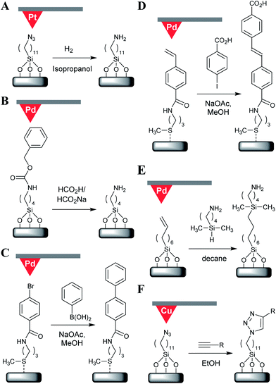
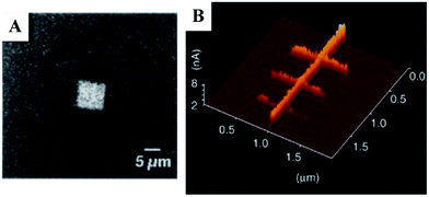
The first example of catalytic scanning probe lithography was reported in 1995 and employed a Pt-coated AFM probe as a hydrogenation catalyst.15 Here, the probe was scanned over an azidosilane self-assembled monolayer (SAM) under H2 saturated isopropanol, resulting in the reduction of the terminal azides to amines (Fig. 1A). The surface feature generated was then treated with amine-specific reagents and fluorescent labels to confirm the azide reduction (Fig. 2A). A tip loading force of 400 nN was required to achieve catalysis (lower loading forces are described only as producing ‘decreased’ levels of catalytic reduction) at a “writing” speed of 1 μm s−1. The loading force was chosen as it represented the force required to penetrate probe/sample solvation layers.Transfer hydrogenations using formic acid as the hydrogen donor have been subsequently reported using Pd-coated probes.16 When this type of hydrogenation was applied to azide reduction, pattern formation occurred at tip-loading forces of 3.0–4.6 μN at speeds up to 5 μm s−1, although trace levels of catalysis were still detectable by fluorescent labelling of terminal amines at up to 10 μm s−1. When applied for the removal of a benzyloxycarbonyl (Cbz) protecting group from an aminosilane SAM (Fig. 1B), this reaction required loading forces above 2.5 μN at 1.5 μm s−1, with no upper speed threshold specified. Under these conditions, both transfer hydrogenation reactions resulted in features with line widths in the 30–40 nm range.
These experiments suggest that larger forces are needed for transfer hydrogenation compared to the use of molecular hydrogen, which may be related to the sensitivity of transfer hydrogenations towards altered temperatures and pressures,30 both of which will be elevated at the point of contact between the probe and surface (see Section 6 below). However, any such effect is also convoluted by the fact that larger forces may be acting to compensate for the faster write speeds employed in these cases.
Probe catalysed thermally induced hydrogenations have also gathered interest more recently in their application to the nanolithography of reduced graphene oxide (rGO) nanoribbons from graphene oxide (GO) using a Pt-coated AFM probe.20 Here, the sample was heated to 115 °C under a H2 atmosphere (0.1 MPa), with lithography successfully performed at tip loading forces of 1–10 nN and speeds of 2–10 nm s−1; with the depth and diameters of the written features being proportional to the loading force, and inversely proportional to write speed. Under optimum conditions features as narrow as 20 nm were reported (Fig. 2B). Notably, this nanolithography method resulted in features that were ∼0.5 nm deep despite the fact that the presented hydroxyl groups and epoxide bridges would only be expected to account for a height difference of 0.1–0.2 nm. This discrepancy is likely to result from height added to the GO surface though a water layer bound to oxygen-containing groups that are absent in the rGO nanoribbons.
Temperature also proved a critical factor in this method of lithography, with pattern formation beginning at 50 °C, improving substantially at 100 °C to reach an optimum at 115 °C (thought to be due to the decreasing prevalence of adsorbed water with elevated temperature). Above 115 °C contrast in electrical conductivity between the rGO features and the surrounding GO declines due to partial thermo-chemical reduction of GO. As an alternative approach, thermochemical nanolithography (TCNL) of GO using an unmodified, heated probe (as opposed to the cSPL approach wherein the entire sample was heated) has been demonstrated.31
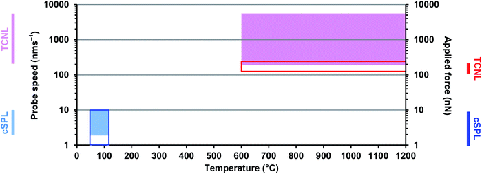
The thermochemical approach required loading forces an order of magnitude greater (120–230 nN vs. 1–10 nN) and considerably higher temperatures (∼600–1200 °C) than the cSPL method. The cSPL approach also achieves conductivities in the rGO nanoribbons 30-fold greater than TCNL, with 2–3 orders of magnitude greater conductivity contrast between the reduced and oxidised regions (cSPL: rGO = 105 S m−1vs. GO = 10−5 to 10−3 S m−1; TCNL: rGO = 103 S m−1vs. GO = 10−1 S m−1). Although the thermochemical lithography was performed under N2 rather than H2, bulk studies on the bulk uncatalysed reduction of GO under Ar/H2 show that temperatures of 800–1000 °C are required for effective reduction.32
Taken together, these data clearly show that the cSPL approach to GO reduction occupies an entirely different parametric space from TCNL (Fig. 3).
2.2 Carbon–carbon and carbon–silicon bond-forming reactions
Transition metal catalysis has been extended to carbon–carbon bond formation and several examples cSPL using Pd-catalysed couplings have been described.17,18,33 In the first example of this concept, biaryl groups were written on an aryl bromide-presenting gold–alkylthiolate SAM by Suzuki coupling (Fig. 1C).17 The probes used in this report were coated with polyvinyl-pyrrolidone (PVP)-coated palladium nanoparticles (PdNP), and required forces of 20–25 nN (at 1 μm s−1) to initiate catalysis. By increasing the scanning speed (to 40 μm s−1) whilst lowering the tip loading force (1–5 nN) the same probe can be used to image the sample non-reactively. A subsequent report18 then demonstrated writing of 10–15 nm biphenyl-amine features on to arylbromide SAMs, requiring 15–20 nN at 1 μm s−1 for catalysis, although some patterning could still be achieved at writing speeds up to 8 μm s−1. This report then extended to demonstrate a probe-directed Heck reaction coupling p-iodobenzoic acid to a styrene-presenting SAM (Fig. 1D), achieving a resolution down to 13 ± 3 nm. Here, catalysis required forces of 25–40 nN at 2 μm s−1, with patterning declining sharply above 3 μm s−1.Subsequent detailed analysis33 revealed that the nature of the Pd coating strongly influenced the performance and lifetime of the probe. Sputter-coated Pd proved incapable of any detectable lithography, electrodeposited Pd irreversibly lost activity after patterning approximately 106 turnovers while PVP–PdNP probes were the most robust; although these also typically irreversibly lost activity after 109 turnovers (patterning of 10's μm2). The limited lifespan was postulated to be due to Ostwald ripening of the Pd surfaces whereby small PdNPs coalesce into larger particles, or rougher surfaces smoothen, resulting in loss of the reactive high-energy surfaces.
It was also found that inverting the Heck coupling (the surface presenting the aryl halide SAM and the styrene in the solution phase) was found to reduce the reaction turnover 3–4 fold. This observation was proposed to be due to the transfer of the rate-determining step (oxidative addition of aryl halide to Pd) from solution phase to the surface, resulting in a retardation of this step due to bulk steric hindrance from the surface. In the Suzuki coupling, changing the SAM's terminal halide from bromine to iodine lowered turnover (from ∼2.1 × 10⁴ to 1.4 × 10⁴ s−1), which may result from aryl bromides having a more negative activation volume than aryl iodides (despite C–Br bonds being stronger than C–I), hence are more responsive to the elevated pressure beneath the probe.
PdNP-catalysed Heck reactions have also been demonstrated using catalytic μCP,34 where the PdNPs were prepared from phase-separated block-copolymer lithography. Features as small as 15 nm could be produced using this catalytically-enabled nanolithography method, which provides a notable alternative strategy to cSPL.
In terms of carbon–silicon bond formation, hydrosilylations involving the addition of aminobutyldimethylsilane to the terminal alkene of octenylsiloxane films (Fig. 1E) have been found to require 2.5 μN of force and could be performed at speeds up to 5 μm s−1 to give line widths of ∼60 nm.16 Pd-catalysed hydrosilylation of terminal alkenes has also been demonstrated using PdNPs immobilised to a μCP stamp35 with a H-terminated Si surface and the alkene as the ink. In this case, a pattern resolution of 20 nm was reported but required 20 min of contact; 6–7 orders of magnitude longer than the ms contact times associated with cSPL hydrosilylation.
2.3 Copper-catalysed ‘click’ ligations
The copper(I)-catalysed azide–alkyne cycloaddition (CuAAC) ‘click’ reaction has been employed to catalytically lithograph surfaces using Cu catalyst immobilised on to AFM probes19 and μCP stamps,36 or deposited as ink in with scanning probes13,37–39 and μCP.36In the cSPL approach,19 a Cu-coated AFM probe was employed to click a range of alkynes to an azidosilane SAM (Fig. 1F), achieving a minimal line width of 50 nm (close to the expected diameter of the metal coated probe). Tip loading forces of 260–300 nN (at 2 μm s−1) proved optimal for catalysis, with higher forces displacing the SAM. It is notable that in comparison to solution phase click reactions that require a reducing agent to produce Cu(I) in situ from a Cu(II) salt, it appears that sufficient Cu(I) is present in the native oxide layer of the probe's Cu coating for catalysis without the need for in situ reduction.
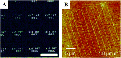
In contrast, there are many examples of DPN-based strategies where the probe deposits a soluble copper catalyst. The first reported example used an AFM probe inked with CuI and an azido-functionalised dendron to write features on to an alkyne-terminated silane surface, which produced written line widths of 300 nm.13 In other examples, the catalytically active Cu(I) ions were produced in situ by using an ink formulation containing CuSO4 and the reducing agent ascorbic acid.37,38 Together with a small molecule azide (e.g. a fluorophore or biotin), features with a width of approximately 85 nm could be produced (Fig. 4A). The use of in situ Cu(II) generation has also been applied to PPL-deposited inks, which offer the advantage of large-area lithography but with the drawback of poorer feature resolution (191 nm reported).39 Thus, feature resolution is poorer with freely diffusing catalytic ink compared to when the catalyst is immobilized to a probe, where catalysis occurs only directly beneath the probe.
2.4 Alkene epoxidation
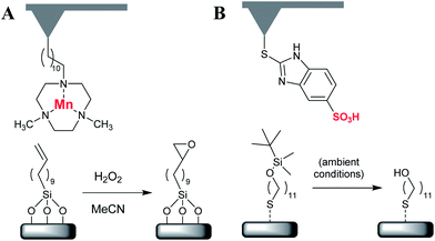
There is currently only one reported example of this type of reaction, which also represents the only current example of “homogenous” catalysis in cSPL.21 This method employs Mn coordinated to 1,3,7-triazacyclononane (tacn) ligands bound to the probe for epoxidation of alkene-terminated SAMs under a solution of H2O2 (Fig. 5A). Writing was performed between 200–600 nN force loads and speeds up to 4.8 μm s−1. Writing produced lines 150–200 nm wide, many times the probe diameter. The reason for this relatively poor resolution remains unclear and may be due to the local release of free manganese into the water meniscus that forms between the probe and substrate under ambient conditions (cf. DPN). It was also noteworthy that writing at 1.2–2.5 μN resulted in both loss of the substrate SAM and irreversible loss of the probe's catalytic activity, presumably through mechanical erosion of the probe-immobilised Mn(tacn) groups.3. Photocatalysis
There have been two of examples of scanning probe-directed photocatalysis. This method relies on the use of TiO2-coated probes, which under UV excitation catalyses the oxidation of adsorbed atmospheric water to generate hydroxide radicals. The underlying chemical reaction for this mode of cSPL is thus not via direct interaction with a catalyst but with an intermediate product. In the first example of this approach,23 TiO2-coated AFM probes were used to pattern features on a surface loaded with microcrystals of the azo dye Procion Red MX-5B. Repeated scanning with TiO2 probe under a UV light source (254 nm) resulted in loss of surface roughness and changes in the UV-vis and IR spectra of the surface, which were used to infer successful catalysis. The process was slow, reaching a plateau of ∼70% decrease in roughness after 6 h of repeated scanning over the same 30 × 30 μm2 area.In a further refinement to the basic concept, TiO2 coated AFM probes and SNOM (scanning near-field optical microscopy) probes coated on their front face were used to photocatalytically pattern gold–alkylthiolate and silane SAMs.24 In the case of the SNOM probes, UV light (325 nm) was directed down the aperture of the probes, thus photocatalytically oxidising the thiol group in a dodecanethiol SAM, allowing replacement with 11-mercaptoundecanoic acid in what could be considered an example of light-driven nanografting. In this report, lateral force microscopy imaging demonstrated a ∼90 nm resolution.
The same researchers also demonstrated the use of “apertureless” photocatalytic lithography using conventional probes coated with TiO2. Here, a beam of light from an HeCd laser is directed on to the apex of the probes. These probes were used to pattern an oligoethylene-presenting silane SAM by oxidative degradation of ethylene glycol units, resulting in the formation of terminal aldehydes (Fig. 4B).24 Subsequent immobilisation of a fluorescent protein (via aminobutylnitrilotriacetic acid and nickel affinity tagging) allowed the generation of ∼70 nm fluorescent patterns. In this case, continuous lines were written at 1.8–2.5 μm s−1, with discontinuous lines observed at 4.0 μm s−1.
4. Non-metal chemocatalysis
In comparison with metal-mediated catalysis, there are fewer examples of organocatalysis in cSPL. The main examples in this category use a tethered strong organic acid to perform probe-localised acid-catalysed reactions. For example, Au-coated probes functionalised with 2-mercapto-5-benzimidazole sulfonic acid have been shown to remove tert-butyldimethylsilyl (TBS) protecting groups from a gold–alkylthiolate SAM to reveal the hydroxy group (Fig. 5B).22 Pattern formation was performed at tip loading forces below 10 nN (with no minimum force specified), with catalysis confirmed by AFM topographic measurements of the reacted SAM. In this case, it is likely that the condensation of a water meniscus at the point of contact between the probe and the surface may facilitate the protonolysis. Nevertheless, the smallest line produced was about 25 nm, which implied that the resolution of the structures was limited only by the contact area beneath the AFM tip (and possible drift in the piezoelectric scanner).The catalytic deprotection of TBS-terminated gold–alkylthiolate SAMs by an immobilized sulfonic acid (2-mercaptoenthane sulfonic acid) has also been performed by μCP, where deprotection was extended to tert-butyloxycarbonyl (Boc)-protected thiols.40,41
5. Enzymatic nanolithography
5.1 Biocatalytic inks
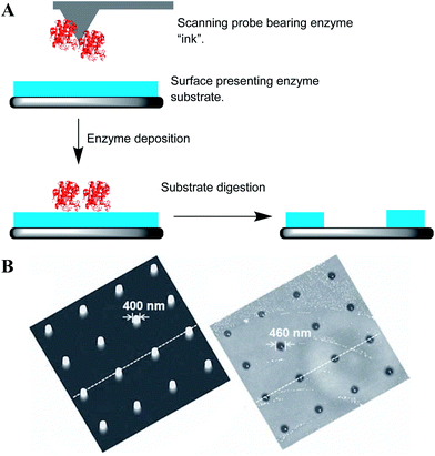
In parallel with transition metal and small molecule catalysis, there has also been significant interest in the use of enzymes with scanning probe nanolithography. Such biocatalysts are attractive since they offer highly efficient catalysis in terms of yields, regio- and stereospecificity; together with their ability to promote reactions under mild conditions.Thus far, the majority of biocatalytic nanolithographies use the probe to deposit free enzyme on to a substrate-presenting surface via DPN or related methods. Subsequent enzymatic digestion of the underlying substrate results in the formation of the nanopatterns (Fig. 6A). This concept has been demonstrated using a number of enzyme systems, including the DPN deposition of DNase I on to a single-stranded DNA monolayer, into which trenches equal in depth to the thickness of the monolayer could be generated with a lateral resolution down to ∼100 nm.11 In other examples, the deposition of proteinase K on to poly-L-lactic acid films14 resulted in features of 400–500 nm (after a 24 h incubation at 37 °C, Fig. 6B), while PPL deposition of Lipase B on poly(ε-caprolactone) films to generated micrometre-scale features (after 7 d incubation at 37 °C).42 In all these cases, the lateral resolution was many fold larger than the probe width, again providing an illustration of the limitations of freely diffusible catalytic inks.
There have also been reports of using nano-fountain pen probes to deliver trypsin solutions. This proteolytic enzyme, when written on to a bovine serum albumin-coated surface enabled the generation of channels ∼100 nm in width under optimum conditions.43,44
However, these examples all essentially describe destructive nanolithography, and necessitates that the surface must first be processed so that it presents the enzyme substrate. As an alternative, enzymatic DPN has also been used in constructive lithography through the deposition of materials on an arbitrary surface to generate features. In this regard, a technique has been reported for the generation of metallic nanowires via DPN deposition of metal NP-conjugated enzymes.12 Here, glucose oxidase (GOx) or galactose oxidase (GalOx) was multiply decorated with 1.4 nm AuNPs and deposited in lines by DPN. The patterned enzyme–NP conjugates were subsequently exposed to their substrates (glucose or galactose) and HAuCl4. The H2O2 generated by the enzyme then acts as a reducing agent to drive Au deposition on to the attached NPs, which increase in size until the enzyme becomes coated by the metal and loses activity. The growing AuNPs also merge into nanowires; 800 nm wide and 220 nm high for GOx, 500 nm wide and 300 nm high for GalOx. A similar process was performed with alkaline phosphatase (AP)–AuNP conjugates, forming a silver nanowire 500 nm wide and 35 nm high, via reduction of AgNO3 by a hydroquinone by-product of p-aminophenylphosphate produced by AP. This approach provides a route to the nanolithography of electrically conducting nanowires, but at the expense of lateral resolution since the growth of the NPs results in line widths typically 10-fold larger than the originally deposited enzyme–AuNP lines.
5.2 Biocatalytic probes
The immobilisation of the enzyme on to a probe or stamp negates the requirement for the ink and thus the need to replace a consumable or increase the complexity of the apparatus by the addition of an ink delivery system (microchannels or reservoirs). Furthermore, it ensures that catalysis takes place only at the point of probe–substrate contact. Biocatalytic lithographies with immobilised enzymes typically rely on covalent attachment of the enzyme to the stamp or probe,25,28,45 but may also use non-covalent approaches, namely the biotin–streptavidin interaction27,29 or through metal affinity with genetically encoded polyhistidine “His-tags”.46Biocatalytic nanolithography with tip-immobilised enzymes for destructive nanolithography was first demonstrated in 2003.25 In this report, endoproteinase V8 was covalently immobilised by bioconjugation to a probe functionalised with succinimide active esters. The enzyme is known to cleave polypeptide chains at C-termini of glutamic acid residues, and could thus be used in combination with a gold–alkylthiolate SAM composed of the peptide A(AEAAKA)6C. Slow scanning of the enzyme-bearing probe across the monolayer (50 nm s−1, roughly 1/20th imaging speed) with the contact force at <50 pN resulted in successful lithography. No lithography was observed at the usual imaging speeds of 1 μm s−1.
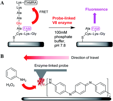
This basic approach was then extended to peptide-coated surfaces where the peptides were labelled with a fluorophore and quencher on either side of the cleavage site (Fig. 7A). Quenching of the fluorophore was relieved upon cleavage at the glutamic acid residue and release of the quencher, resulting in fluorescence from the hydrolysed regions.26,28 Notably, the generation of fluorescent features (i.e. successful lithography) only occurred when the probe was first etched with a focused ion beam to remove a large part of the apex of the cantilever, leaving a truncated pyramid presenting a triangular surface on to which the enzyme was attached. Using a fixed loading force of 1.2 nN, no fluorescence was observed with a probe that had not been etched. The need for this ∼10![[thin space (1/6-em)]](https://www.rsc.org/images/entities/char_2009.gif) 000 fold increase in probe–substrate contact area provided by the etching (∼600 nm2 for the unmodified probe, ∼11 μm2 for the etched probe) strongly suggested that the immobilised enzymes were poorly active. Indeed, a subsequent investigation of enzyme activity by comparing the similar amounts of the enzyme immobilised on to silicon nanoparticles using the same bioconjugate chemistry and the free enzyme revealed that V8 retained only ∼20% activity following covalent immobilisation.
000 fold increase in probe–substrate contact area provided by the etching (∼600 nm2 for the unmodified probe, ∼11 μm2 for the etched probe) strongly suggested that the immobilised enzymes were poorly active. Indeed, a subsequent investigation of enzyme activity by comparing the similar amounts of the enzyme immobilised on to silicon nanoparticles using the same bioconjugate chemistry and the free enzyme revealed that V8 retained only ∼20% activity following covalent immobilisation.
It is interesting to note that the same research team attempted to immobilise His-tagged V8, at either the N- or C-termini of the protein, on to nitrilotriacetic acid-modified AFM probes, but found that activity was lost in both cases. Addition of a His-tag to the N-terminus would be expected to abolish activity, as the N-terminal valine interacts directly with active site of the enzyme. The C-terminus, however, is on the opposite side of the molecule, and a His-tag here would be expected to present the enzyme to the substrate at a near-ideal orientation. The reasons for this observation remain unclear but may have implications for future attempts at improving immobilised enzyme activity though control of orientation.
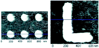
Probe immobilised enzymes have also been used to demonstrate constructive nanolithography. This concept was first demonstrated with AP immobilised on to probes.27 When the enzyme is treated with a mixture of 5-bromo-4-chloro-3′-indolyphosphate (BCIP) and nitro-blue tetrazolium (NBT), dephosphorylation of BCIP reduces NBT to insoluble NBT diformasan. The nanolithography is thus performed by the precipitation of the reaction product as the probe is traced across the surface, with lateral resolutions of 150–170 nm being reported (Fig. 8).
A further development in this area was the use of probe-immobilised horseradish peroxidase (HRP) for the nanolithographic deposition of polyaniline, a flexible, biocompatible and electrically conductive polymer.29 Here, the HRP catalysed the oxidative polymerisation of aniline with H2O2 (Fig. 7B). This report is particularly notable as although the deposition of NBT diformasan was an interesting proof of concept, the material used to form the features was of little use for further application. Instead, the generation of nanoscale polyaniline patterns of arbitrary geometry may prove a step towards the fabrication of biosensors, implants and nanoelectronics.
In both cases, attachment of the enzyme only to the apex of the probe was critical for such constructive lithographies since the presence of the enzyme on any other part of the probe would result in the deposition of the material across the entire surface of the probe. In order to confine the attachment of the enzyme only to the apex of the probe, the entire probe was first functionalised with biotin, a small molecule biological cofactor that is strongly bound by the protein streptavidin. The probe is then scanned across a surface bearing the enzyme–streptavidin conjugate, resulting in the ‘pick-up’ of the enzymes only at the point of contact.
6. Rationalisation of lithography parameters
Under optimum conditions cSPL is capable of patterning resolutions comparable those achieved by the other scanning probe lithographies (<50 nm). In contrast to methods involving the deposition of inks containing catalysts, tip loading force is the parameter most critical to successful cSPL, with catalysis routinely described as occurring only within a specific ‘force window’. In general, cSPL is usually performed at higher loading forces and lower probe velocities than those used for imaging, but the interplay between speed, force applied and temperature is complex.The moving catalyst must make and maintain physical contact with the substrate, penetrating any solvation layers present, and maintain a sufficient contact area to catalyse features of detectable width (often the presence of features must be inferred through subsequent elaboration, typically with a bulky molecular species or fluorophore). In examples using metallic or small molecule catalysts, the upper force threshold does not represent a level of force inhibitory to catalysis, but is the force above which mechanically displaces the substrate from the surface (>70 nN for alkylthiolate SAMs on gold, >400 nN for siloxanes).16–18,21 At forces approaching this threshold catalysis and displacement will occur concurrently, thus the ideal force for pattern formation must lie significantly below that required for displacement.
At the nanoscale contact areas involved, the application of tip loading forces in the nN–μN range have been calculated to generate GPa local pressures.16,33 Furthermore, the tip–substrate frictional (shear) forces, and the temperature at the site of catalysis may be significantly higher than room temperature and contribute to the acceleration of local chemical reactions. Experiments using μCP stamps with immobilised PdNPs required a temperature of 130 °C and 30 min contact time induce Heck coupling reactions,34 whilst AFM-immobilised PdNPs performed the reaction without external heating and with only millisecond catalyst–substrate contact times.18 However, any rate enhancement provided by friction alone is insufficient to compensate for the reduction in contact duration accompanying increased writing speed, as feature size is universally observed to be inversely proportional to writing speed. This observation suggests that at low speeds, increased catalyst–substrate contact time will offset reductions in pressure/temperature; hence there are no reports of minimal writing speeds.
Enzymatic cSPL requires much slower speeds than cSPL with non-enzyme catalysts with <0.3 μm s−1 and 1–5 μm s−1 respectively for the cases discussed above, although due to wide range of reactions presented it is difficult to make direct head-to-head comparisons. Enzyme turnover rates are typically orders of magnitude higher than non-enzyme catalysts, however the size of enzymes will necessarily mean that the probe apex will present considerably fewer catalytically active species than a metal-coated probe. For example, a probe with a radius of curvature of 10 nm may be considered to end in a half spherical cap with a surface area of ∼628 nm2. If this were a Pt-coated probe (assuming a van der Waals radius of 0.175 nm for Pt and ideal surface packing), it would present ∼6000 Pt atoms on its surface. If this was the same probe decorated with V8 proteinase, ∼32 enzymes would occupy the same area. Assuming the probe fully penetrates a 1.5 nm thick substrate monolayer (an approximation for both an azidosilane and a 10-mer peptide), that equates to ∼1000 Pt atoms or 5 proteinase molecules in contact with the substrate. The cSPL of azidosilanes using a Pt probe15 was performed at 1 μm s−1 and peptide cSPL with V8 was performed at 50 nm s−1, thus it appears that having 200-fold less catalyst requires only a 20-fold decrease in writing speed to perform a broadly similar end result – the creation of a micron-scale square amenable to subsequent fluorescent labelling showing high contrast against the background.
Comparisons between atomic and enzymatic catalysts on probes is further complicated by the fact that the actual site of catalysis remains unclear and desorbed metal atoms may in fact be the key catalytic species and the lithography is not be strictly confined to the probe–surface interface. Davis et al.33 proposed the PVP–PdNPs employed on their probes produced a diffuse ‘cloud’ of Pd atoms complexed to the PVP shell. Evidence for this leaching of metals from the probe is offered by the fact that high levels of background catalysis could be prevented with the addition of chelators to scavenge any leached metals.16 Furthermore, similar systems employing Pd-coated μCP stamps have shown transfer of Pd to the surface.34
Pre-treatment of both the probes prior to nanolithography is also influential. For example, annealing of TiO2-coated probes24 promotes phase transition of TiO2 to the more catalytically active anatase phase. Overnight air curing of Cu-coated probes19 yielded substantial improvements in activity, whilst Cu-coated μCP stamps were measured to be 5 times more active following similar overnight curing,36 likely due to the formation of a native oxide layer containing catalytically active Cu(I) ions. Preparation of the surfaces prior to nanolithography is also an important factor. Vacuum curing of the siloxane SAMs16 was shown to improve patterning resolution (from 200 nm to 30–40 nm) through the promotion of silanol condensation, improving monolayer ordering and stability, permitting writing to occur at greater loading forces (thus a greater rate of catalysis) before displacement of the SAM occurs.
A more practical consideration is the limited lifespan of immobilised catalysts. Wherever tested, both cSPL probes21,28,33 and μCP stamps34,36,45,47 were found have lost most or all of their activity with repeated use (typically 10's μm2 of scanned area for cSPL probes and 4–6 uses for catalytic μCP stamps). For metallic coatings, it appears that the loss of activity is not simply due to the absolute loss of catalyst due to leaching but also the loss of highly reactive catalytic sites, possibly due to Ostwald ripening (see Section 2.2 above). In the case of enzymes, it seems likely that the loss of activity is due to the unfolding (denaturation) of the enzyme under the high shear forces and pressures generated by the moving probe.
7. Conclusions and outlook
There have now been many reports that convincingly demonstrate the chemical scope of cSPL and the flexibility of combining chemical specificity of catalysis with the positional specificity of SPM.However, the vast majority of the reported examples are proof-of-concept studies. In order for these methods to be more widely applied to practical applications, a number of issues remain to be addressed such as the limited probe lifespan and more convenient probe functionalisation methods in the case of molecular or enzymatic catalysts. Detailed studies of the physical conditions present at the probe tip will also be crucial to understanding the mechanisms of catalysis and experimental parameter optimisation, which in turn are necessary for the development of improved cSPL systems. For example, uncertainties regarding the temperatures generated during writing could be measured by the use of thermocouple AFM probes, which have been fabricated with both Pt and Pd as the thermocouple junctions on the probe apex.48,49 As such they would be catalytically active across a range of surface chemistries and would allow in situ monitoring of the temperature.
Looking to the future, parallelisation through the use of arrays of multiple probes (e.g. through PPL or HSL) to enable higher lithographic throughput and large-area fabrication is one clear direction for maturation of the technology, particularly in nanoelectronics production. In a similar manner, beam pen lithography and the Snomipede offer future routes towards the multiplexing of photocatalytic reactions.50,51
Spatial resolution may be substantially enhanced by the use of single enzymes or single NPs at the probe apex. For example, methods already exist for single NPs to be synthesised at AFM probe apices.52 In the case of enzymatic cSPL, there are now powerful directed evolution methods that enable the rapid generation of highly active enzymes.53 Such genetic recombinant methods could be utilised to generate and select enzymes specifically for cSPL applications. Biocatalytic cSPL would also benefit from harnessing improved site-specific enzyme immobilisation methods,54,55 to ensure that the enzymes attached to the probes retain maximum activity. This aspect is particularly crucial for nanoscale applications where relatively few protein molecules can be located on a single nanoscale object. A conceptually interesting but more speculative avenue would be the use of diffusion-limited enzymes56,57 (where catalysis occurs so rapidly the reaction rate is limited by the rate of diffusion of reactants) would make excellent candidates for probe mounted catalysts, as the enzyme could be presented with substrate at a rate greater than that possible by diffusion, potentially enabling extremely rapid lithography.
In summary catalytic scanning probe lithography combines the chemical specificity of catalysis with the positional specificity of SPM, and has achieved patterning precisions approaching those of many classical SPL techniques. Although there are still obstacles to be overcome, with refinements to throughput, resolution and probe lifespan, the technique potentially represents a disruptive manufacturing technology and a step towards an efficient, compact and universal “desk-top fab”.
Acknowledgements
The authors acknowledge financial support from the UK Engineering and Physical Sciences Research Council (EP/K011685/1, EP/K024485/1).Notes and references
- B. D. Gates, Q. Xu, M. Stewart, D. Ryan, C. G. Willson and G. M. Whitesides, Chem. Rev., 2005, 105, 1171–1196 CrossRef CAS PubMed.
- H. Sugihara, A. Takahara and T. Kajiyama, J. Vac. Sci. Technol., B: Microelectron. Nanometer Struct.–Process., Meas., Phenom., 2001, 19, 593–595 CrossRef CAS.
- S. Xu and G.-y. Liu, Langmuir, 1997, 13, 127–129 CrossRef CAS.
- H. C. Day and D. R. Allee, Appl. Phys. Lett., 1993, 62, 2691–2693 CrossRef CAS PubMed.
- W.-K. Lee, M. Haydell, J. T. Robinson, A. R. Laracuente, E. Cimpoiasu, W. P. King and P. E. Sheehan, ACS Nano, 2013, 7, 6219–6224 CrossRef CAS PubMed.
- L. R. Giam and C. A. Mirkin, Angew. Chem., Int. Ed., 2011, 50, 7482–7485 CrossRef CAS PubMed.
- K. Salaita, Y. Wang and C. A. Mirkin, Nat. Nanotechnol., 2007, 2, 145–155 CrossRef CAS PubMed.
- L. R. Giam, A. J. Senesi, X. Liao, L. S. Wong, J. Chai, D. J. Eichelsdoerfer, W. Shim, B. Rasin, S. He and C. A. Mirkin, Proc. SPIE, 2011, 8031, 803103 CrossRef PubMed.
- A. Lewis, Y. Kheifetz, E. Shambrodt, A. Radko, E. Khatchatryan and C. Sukenik, Appl. Phys. Lett., 1999, 75, 2689–2691 CrossRef CAS PubMed.
- S. Asmahan, K. Wonmo, C. David, D. Ralu, M. Nicolae and D. E. Horacio, J. Micromech. Microeng., 2013, 23, 125014 CrossRef.
- J. Hyun, J. Kim, S. L. Craig and A. Chilkoti, J. Am. Chem. Soc., 2004, 126, 4770–4771 CrossRef CAS PubMed.
- B. Basnar, Y. Weizmann, Z. Cheglakov and I. Willner, Adv. Mater., 2006, 18, 713–718 CrossRef CAS PubMed.
- D. A. Long, K. Unal, R. C. Pratt, M. Malkoch and J. Frommer, Adv. Mater., 2007, 19, 4471–4473 CrossRef CAS PubMed.
- H. Li, Q. He, X. Wang, G. Lu, C. Liusman, B. Li, F. Boey, S. S. Venkatraman and H. Zhang, Small, 2011, 7, 226–229 CrossRef CAS PubMed.
- W. T. Müller, D. L. Klein, T. Lee, J. Clarke, P. L. McEuen and P. G. Schultz, Science, 1995, 268, 272–273 Search PubMed.
- C. Blackledge, D. A. Engebretson and J. D. McDonald, Langmuir, 2000, 16, 8317–8323 CrossRef CAS.
- J. J. Davis, K. S. Coleman, K. L. Busuttil and C. B. Bagshaw, J. Am. Chem. Soc., 2005, 127, 13082–13083 CrossRef CAS PubMed.
- J. J. Davis, C. B. Bagshaw, K. L. Busuttil, Y. Hanyu and K. S. Coleman, J. Am. Chem. Soc., 2006, 128, 14135–14141 CrossRef CAS PubMed.
- W. F. Paxton, J. M. Spruell and J. F. Stoddart, J. Am. Chem. Soc., 2009, 131, 6692–6694 CrossRef CAS PubMed.
- K. Zhang, Q. Fu, P. Nan, X. Yu, J. Liu, Y. Luo, X. Wang, J. Yang and J. Hou, Nat. Commun., 2012, 3, 1194 CrossRef PubMed.
- D. A. Valyaev, S. Clair, L. Patrone, M. Abel, L. Porte, O. Chuzel and J.-L. Parrain, Chem. Sci., 2013, 4, 2815–2821 RSC.
- M. Péter, X.-M. Li, J. Huskens and D. N. Reinhoudt, J. Am. Chem. Soc., 2004, 126, 11684–11690 CrossRef PubMed.
- V. Zorbas, M. Kanungo, S. A. Bains, Y. Mao, T. Hemraj-Benny, J. A. Misewich and S. S. Wong, Chem. Commun., 2005, 4598–4600 RSC.
- E. Ul-Haq, S. Patole, M. Moxey, E. Amstad, C. Vasilev, C. N. Hunter, G. J. Leggett, N. D. Spencer and N. H. Williams, ACS Nano, 2013, 7, 7610–7618 CrossRef CAS PubMed.
- S. Takeda, C. Nakamura, C. Miyamoto, N. Nakamura, M. Kageshima, H. Tokumoto and J. Miyake, Nano Lett., 2003, 3, 1471–1474 CrossRef CAS.
- C. Nakamura, C. Miyamoto, I. Obataya, N. Nakamura and J. Miyake, Proc. SPIE, 2004, 5593, 277–283 CrossRef PubMed.
- L. Riemenschneider, S. Blank and M. Radmacher, Nano Lett., 2005, 5, 1643–1646 CrossRef CAS PubMed.
- C. Nakamura, C. Miyamoto, I. Obataya, S. Takeda, M. Yabuta and J. Miyake, Biosens. Bioelectron., 2007, 22, 2308–2314 CrossRef CAS PubMed.
- X. Luo, V. A. Pedrosa and J. Wang, Chem.–Eur. J., 2009, 15, 5191–5194 CrossRef CAS PubMed.
- R. A. W. Johnstone, A. H. Wilby and I. D. Entwistle, Chem. Rev., 1985, 85, 129–170 CrossRef CAS.
- Z. Wei, D. Wang, S. Kim, S.-Y. Kim, Y. Hu, M. K. Yakes, A. R. Laracuente, Z. Dai, S. R. Marder, C. Berger, W. P. King, W. A. de Heer, P. E. Sheehan and E. Riedo, Science, 2010, 328, 1373–1376 CrossRef CAS PubMed.
- D. Yang, A. Velamakanni, G. Bozoklu, S. Park, M. Stoller, R. D. Piner, S. Stankovich, I. Jung, D. A. Field, C. A. Ventrice, Jr and R. S. Ruoff, Carbon, 2009, 47, 145–152 CrossRef CAS PubMed.
- J. J. Davis and Y. Hanyu, Nanotechnology, 2010, 21, 265302 CrossRef PubMed.
- H. Mizuno and J. M. Buriak, ACS Appl. Mater. Interfaces, 2010, 2, 2301–2307 CAS.
- H. Mizuno and J. M. Buriak, J. Am. Chem. Soc., 2008, 130, 17656–17657 CrossRef CAS PubMed.
- J. M. Spruell, B. A. Sheriff, D. I. Rozkiewicz, W. R. Dichtel, R. D. Rohde, D. N. Reinhoudt, J. F. Stoddart and J. R. Heath, Angew. Chem., Int. Ed., 2008, 47, 9927–9932 CrossRef CAS PubMed.
- H.-Y. Chen, M. Hirtz, X. Deng, T. Laue, H. Fuchs and J. Lahann, J. Am. Chem. Soc., 2010, 132, 18023–18025 CrossRef CAS PubMed.
- S. Oberhansl, M. Hirtz, A. Lagunas, R. Eritja, E. Martinez, H. Fuchs and J. Samitier, Small, 2012, 8, 541–545 CrossRef CAS PubMed.
- S. Bian, J. He, K. B. Schesing and A. B. Braunschweig, Small, 2012, 8, 2000–2005 CrossRef CAS PubMed.
- A. A. Shestopalov, R. L. Clark and E. J. Toone, Nano Lett., 2009, 10, 43–46 CrossRef PubMed.
- A. A. Shestopalov, R. L. Clark and E. J. Toone, Langmuir, 2009, 26, 1449–1451 CrossRef PubMed.
- M. Ganesh, J. Nachman, Z. Mao, A. Lyons, M. Rafailovich and R. Gross, Biomacromolecules, 2013, 14, 2470–2476 CrossRef CAS PubMed.
- R. E. Ionescu, R. S. Marks and L. A. Gheber, Nano Lett., 2003, 3, 1639–1642 CrossRef CAS.
- R. E. Ionescu, R. S. Marks and L. A. Gheber, Nano Lett., 2005, 5, 821–827 CrossRef CAS PubMed.
- A. l. Guyomard-Lack, N. Delorme, C. l. Moreau, J.-F. o. Bardeau and B. Cathala, Langmuir, 2011, 27, 7629–7634 CrossRef CAS PubMed.
- P. W. Snyder, M. S. Johannes, B. N. Vogen, R. L. Clark and E. J. Toone, J. Org. Chem., 2007, 72, 7459–7461 CrossRef CAS PubMed.
- X.-M. Li, M. Péter, J. Huskens and D. N. Reinhoudt, Nano Lett., 2003, 3, 1449–1453 CrossRef CAS.
- K. Luo, Z. Shi, J. Lai and A. Majumdar, Appl. Phys. Lett., 1996, 68, 325–327 CrossRef CAS PubMed.
- K. Luo, Z. Shi, J. Varesi and A. Majumdar, J. Vac. Sci. Technol., B: Microelectron. Nanometer Struct.–Process., Meas., Phenom., 1997, 15, 349–360 CrossRef CAS.
- F. Huo, G. Zheng, X. Liao, L. R. Giam, J. Chai, X. Chen, W. Shim and C. A. Mirkin, Nat. Nanotechnol., 2010, 5, 637–640 CrossRef CAS PubMed.
- E. ul-Haq, Z. Liu, Y. Zhang, S. A. Alang Ahmad, L. S. Wong, J. K. Hobbs, G. J. Leggett, J. Micklefield, C. J. Roberts and J. M. R. Weaver, J. Mater. Res., 2011, 26, 2997–3008 CrossRef CAS.
- H. Wang, T. Tian, Y. Zhang, Z. Pan, Y. Wang and Z. Xiao, Langmuir, 2008, 24, 8918–8922 CrossRef CAS PubMed.
- M. T. Reetz, J. Biomed. Sci. Eng., 2011, 50, 138–174 CAS.
- L. S. Wong, F. Khan and J. Micklefield, Chem. Rev., 2009, 109, 4025–4053 CrossRef CAS PubMed.
- L. S. Wong, C. V. Karthikeyan, D. J. Eichelsdoerfer, J. Micklefield and C. A. Mirkin, Nanoscale, 2012, 4, 659–666 RSC.
- S.-X. Lin and J. Lapointe, J. Biomed. Sci. Eng., 2013, 6, 435–442 CrossRef CAS.
- G. Zhou, M.-T. Wong and G.-Q. Zhou, Biophys. Chem., 1983, 18, 125–132 CrossRef CAS.
| This journal is © The Royal Society of Chemistry 2014 |

