 Open Access Article
 This Open Access Article is licensed under a
 Creative Commons Attribution 3.0 Unported Licence
DNA-templated nanowires: morphology and electrical conductivity
Scott M. D.
Watson
,
Andrew R.
Pike
,
Jonathan
Pate
,
Andrew
Houlton
and
Benjamin R.
Horrocks
*
Chemical Nanoscience Laboratory, School of Chemistry, Bedson Building, Newcastle University, Newcastle Upon Tyne, NE1 7RU, UK. E-mail: b.r.horrocks@ncl.ac.uk
First published on 26th February 2014
Abstract
DNA-templating has been used to create nanowires from metals, compound semiconductors and conductive polymers. The mechanism of growth involves nucleation at binding sites on the DNA followed by growth of spherical particles and then, under favourable conditions, a slow transformation to a smooth nanowire. The final transformation is favoured by restricting the amount of templated material per unit length of template and occurs most readily for materials of low surface tension. Electrical measurements on DNA-templated nanowires can be facilitated using three techniques: (i) standard current–voltage measurements with contact electrodes embedded in a dielectric so that there is a minimal step height at the dielectric/electrode boundary across which nanowires may be aligned by molecular combing, (ii) the use of a dried droplet technique and conductive AFM to determine contact resistance by moving the tip along the length of an individual nanowire and (iii) non-contact assessment of conductivity by scanned conductance microscopy on Si/SiO2 substrates.
1 Introduction
DNA is an effective template for the formation of nanowires (NWs) by wet chemical methods because it is available as extremely monodisperse samples with exceptional control over the length (in multiples of base-pairs) and it is chemically robust. DNA will retain its basic structural integrity under the reaction conditions necessary to form metals, semiconductors and conductive polymers as long as neither strong acids nor high temperatures are required. In addition, much is known about the metal-binding chemistry of nucleic acids1 and this chemistry has been exploited to make a wide range of inorganic materials (Fig. 1). Further, hydrophobic organic molecules interact strongly with DNA, often via the minor groove, and the analogy between such molecules and the oligomers of nascent conductive polymers such as poly(pyrrole) and poly(aniline) has been used to make long conductive polymer NWs by DNA-templating.2–4 This interaction is partly electrostatic between the cationic conductive polymer and the anionic phosphate backbone of DNA, but salt formation alone does not explain the success of the process, because other potential polyanionic templates such as high molecular weight poly(styrene sulfonate) are much less effective. As well as additional favourable interactions with the hydrophobic minor groove, the relative stiffness of DNA is also important. The persistence length of dsDNA is of the order of 50 nm (ref. 5) and therefore it does not form the sort of globular structures that more flexible synthetic polymers do at high ionic strength. | ||
| Fig. 1 (a) Ball and stick model of duplex DNA. The colour scheme for the atoms is O (red), P (purple), C (grey) and N (blue). (b) Schematic illustrating possible binding modes of metal ions (to the phosphate groups and the nitrogen atoms of the nucleobases) and of short oligomers (in the minor groove). Binding of these species facilitates the nucleation of metals (M0), binary semiconductors (MS) and conductive polymers (e.g., poly(pyrrole)) on the DNA template. | ||
DNA does have significant limitations as a template; principally these relate to its lack of solubility in nearly all organic solvents and it cannot tolerate temperatures much greater than about 200 °C in air. This means that some desirable NW materials, e.g., silicon & gallium arsenide have not been prepared on a DNA template and other techniques such as vapour–liquid–solid (VLS) growth are superior routes to such NWs at present.6 It is possible to immobilise DNA on a solid surface, e.g., mica, prior to templating and then carry out the templating reaction in a drop of solvent on the mica surface. However, as discussed below, we typically find that the same reaction carried out in bulk solution with freely-dissolved DNA molecules can produce very different products than that carried out under identical conditions, but with the DNA immobilised on a solid support.7 Several reviews are available, which deal with details of the chemistries that have been employed and the applications of metallic and semiconducting DNA-templated NWs.8–11 In this feature article we will give a brief overview of the types of materials that have been templated on DNA and then we will focus on our work concerned with the NW growth mechanism and the development of techniques for the study of the electrical properties of the NWs.
1.1 Metals
A broad range of metals have been templated on DNA; examples include Ag,12–14 Au,15–17 Pt,18 Cu,19,20 Ni,21 Fe,22 Co23 and Pd,24,25 although not all of these form smooth and conductive NWs. The typical reaction involves mixing DNA with a solution of a metal salt and then adding a reducing agent. The DNA may be dissolved in solution, or immobilised on a solid substrate. Metal templating on DNA usually involves aqueous reactions, however organic solvents may be used if the DNA is first aligned by molecular combing on a solid substrate, e.g., mica or Si/SiO2. For example, we have incubated such substrates with a solution of tetrakis(acetonitrile)copper(I) hexafluorophosphate ([Cu(CH3CN)4][PF6]) (10 mM, 1 mL, dry CH3CN) in a Schlenk flask for 20 minutes to afford Cu(I) doped DNA. The copper salt was reduced to the metal by dropwise addition of phenylsilane (PhSiH3) (20 mM, 1 mL, dry CH3CN) and the sample was washed with dry acetonitrile and dried under a flow of nitrogen to leave immobilised Cu/DNA NWs.26Metal ions bind strongly to DNA at a variety of sites by electrostatic interaction with the phosphate groups and by coordination to the nucleobases. The metal nuclei can therefore form on the template18 and growth occurs to produce larger metal NPs,12 which under appropriate conditions will eventually coalesce to produce a conductive NW. It should be noted that this process is distinct from the interaction of pre-formed metal nanoparticles with a DNA molecule, which is a common, but distinct, strategy for the formation of assemblies of individual nanoparticles.27,28 More sophisticated variations on the basic method include the use of Pt29,30 or Pd31,32 seeds in a manner analogous to techniques used to prepare Cu interconnects as part of the Damascene process. Metallisation of more complex DNA structures13,14 and DNA origami33 has also been demonstrated.
The metal![[thin space (1/6-em)]](https://www.rsc.org/images/entities/char_2009.gif) :DNA ratio is a crucial parameter in all these reactions; if it is too small, i.e., if there is no excess of metal in the solution and all is bound to the DNA, then metal NPs rather than a continuous NW will be formed. On the other hand, if the metal:DNA ratio is large then well-defined NWs may not be formed either. The stoichiometry of the reaction is discussed below in the coarse-grained thermodynamic model of Section 2.2.
:DNA ratio is a crucial parameter in all these reactions; if it is too small, i.e., if there is no excess of metal in the solution and all is bound to the DNA, then metal NPs rather than a continuous NW will be formed. On the other hand, if the metal:DNA ratio is large then well-defined NWs may not be formed either. The stoichiometry of the reaction is discussed below in the coarse-grained thermodynamic model of Section 2.2.
1.2 Semiconductors
Many binary semiconductors are straightforward to template on DNA by precipitation of the metal ion with a suitable source of the chalcogenide or hydroxide.10 In the case of CdS, the early work was mainly concerned with the use of DNA to stabilise quantum-confined CdS particles (Q-CdS)34 and this remains an active area.35 Instead, CdS NWs have been prepared by addition of Cd2+ ions to a solution of λ-DNA followed by reaction with HS− from aqueous sodium sulfide and allowing the reaction solution to stand.7 ZnS has also been prepared by the simple precipitation route.36 Other metal sulfides, e.g., CuS37 and PbS38 can be prepared by the obvious generalisations and have interesting optical properties, although the conductivity of these structures was not determined. Magnetite NWs (Fe3O4/DNA) have been prepared by addition of hydroxide ions to a 1:1.5 mixture of Fe(II):Fe(III) in the presence of DNA.39
Nanoscale cuprous oxide is of interest because of the unusual optical properties of bulk Cu2O which have been studied in great detail.40,41 The simplest way to prepare Cu2O NWs on a λ-DNA template is to allow Cu(II) ions to bind to the template in aqueous citrate (Benedict's reagent) and then to reduce the Cu(II) to Cu(I) by addition of ascorbate.42 A recent, alternative approach to certain binary compounds is based on galvanic displacement; DNA was seeded with Ag and then Cu or Ni NWs formed by electroless plating and finally the metal NW was dissolved in an acidic solution of HTeO2+ or HTeO2+ & Bi3+. This procedure produces either Te/DNA or Bi2Te3/DNA NWs and is of particular interest because such materials cannot easily be prepared by the simple precipitation route from aqueous solution.43 Finally, an electrochemical deposition technique has been used to prepare CdSe on single-stranded DNA templates.44
As for the metal NWs, not all of these systems have been characterised electrically, although CdS/DNA NWs have been aligned by combing on substrates and observed to be quite conductive7 and flexible.45
1.3 Conductive polymers
Many aromatic heterocycles are polymerised upon oxidation. Pyrrole, aniline, thiophene, indole and their derivatives are typical examples. The mechanism is generally considered to involve dimerisation of the initial radical cations followed by loss of protons and reoxidation of the dimer, which typically has a lower oxidation potential than the monomer. The polymerisation proceeds by further coupling of radical cations to the oxidised oligomers and eventually the polymer becomes insoluble as the molecular weight increases. This type of polymerisation maybe carried out electrochemically or using chemical oxidants such as ferric chloride. The polymer is cationic as-formed and the oligomers bear some resemblance to minor groove binding molecules such as Hoechst 33258 (charged aromatic heterocycles). Examples of such DNA-templated conductive polymers include poly(aniline),2,3 poly(pyrrole),4 poly(dithienylpyrrole)46 and poly(indole).47 Conductive polymers are particularly attractive materials to template on DNA because they form smooth, conductive NWs and they provide access to a wide range of chemical functionality for subsequent applications.Whilst inorganic NWs are may be functionalised using methods originally developed for bulk substrates, e.g., oxide/chlorosilane or gold/thiol chemistries, the polymer NWs can be functionalised simply by derivatisation of the monomer and the density of functional groups adjusted by copolymerisation. This method has been used to incorporate alkynyl groups to enhance the nucleation of subsequent Ag layers,48 or to allow the functionalisation of the NWs by the copper-catalysed azide–alkyne Huisgen cycloaddition, ‘click’, reaction.49
2 Structure of DNA-templated nanowires and the mechanism of templating
The details of the mechanism of DNA-templating are of fundamental interest, but also have significance for the major proposed applications of NWs as interconnects in electronic devices and as transducing elements in chemical sensors. In the case of interconnects, it is clearly desirable for the NWs to be uniform and continuous to attain the maximum possible conductivity. For sensing, where the signal is typically the fractional change in conductivity upon exposure to the analyte, it may be more important for the NW to have a high surface:volume ratio in order to maximise the sensitivity and therefore a uniform, smooth morphology is not necessarily optimal.
DNA-templated NWs show a range of morphologies: some are smooth and uniform, whereas other examples show a dendritic structure and may be hard to recognize in AFM or TEM as individual wires. The morphology observed typically depends on both the preparation conditions and the material that is templated. CdS NWs may be prepared which appear uniform in AFM images and which may be combed across gold contacts to form a simple two-terminal device. These CdS NWs have a conductivity of the order of 3 S cm−1 (in the absence of a contact resistance measurement, this is a lower bound (ref. 7)), which confirms the contiguous nature of the templated material. The preparation involves deposition of CdS on freely-dissolved DNA molecules, followed by a slow annealing step. In contrast, CdS templated on DNA under similar conditions, but where the annealing step is omitted, or the DNA molecules are immobilized on mica during the templating reaction, tends to form electrically-insulating beads-on-a-string structures.7 We have found the transition between the beads-on-a-string morphology and the smooth NWs illustrated in Fig. 2 to be a common phenomenon in DNA-templated materials7,10,42 and others have also observed similar effects in templating, e.g., Au on synthetic polymer molecules.50
 | ||
| Fig. 2 Schematic illustration of the transformation from a beads-on-a-string morphology to a smooth nanowire observed in many DNA-templating studies and described by the model represented by eqn (4). The DNA template is shown as a green cylinder and the templated material as blue. (a) Spherical nuclei formed on the template by reduction or precipitation of metal ions, or oligomerisation of heterocyclic monomers. (b) Formation of ‘necks’ between the particles as material is transferred from the particles to the regions of bare template. (c) Under the condition of eqn (2) the equilibrium state is a smooth nanowire of uniform thickness, although the approach to equilibrium is slow. | ||
Most investigations of DNA-templated NW structure rely heavily on AFM, although TEM is often also used to characterise inorganic NWs.36,37,44 For AFM studies DNA-templated NWs may be aligned on a substrate in a manner similar to bare DNA molecules.51 So-called ‘molecular combing’ involves the extension and alignment of the molecule by a receding meniscus; it can be performed very simply by dragging a droplet containing a suspension of NWs with the tip of a micropipette across a flat substrate. Si/SiO2 chips are ideal and the oxide is often silanized to increase the hydrophobicity of the surface and reduce the adhesion of the NWs to the substrate.52 NW diameters estimated from the heights in AFM images lie in the range 5–20 nm; bare λ-DNA is well-known to show apparent heights of 1 nm or less in such AFM images owing to substrate interactions and tip/substrate effects. The NW diameters are towards the lower end of the ranges accessible by other synthetic methods, for example templating conductive polymers in porous alumina53 typically produces wires of diameter ≥10 nm and VLS growth of crystalline semiconductors produces wires 20–100 nm in diameter,6 although laser-ablation techniques can be used to reduce the size of the metal catalyst particles and therefore of the Si NWs to 6 nm diameter.54 We do not usually observe individual DNA-templated NWs thicker than about 20 nm for any of the materials we have studied (metals, sulfides, oxides, conductive polymers) and we interpret this in terms of a coarse-grained model of NW formation discussed below. We do occasionally observe very thick ≳50 nm diameter wires if the NWs are prepared in suspension and left in the reaction solution for long times (hours–days).42,47,52 This is not due to the formation of thick individual wires, but instead arises from the formation of assemblies in which individual NWs wrap around each other as the strands in a rope.52 These ropes are very easily observed in AFM because the individual NWs that comprise the strands can be resolved in regions where the rope has unravelled (Fig. 3). The driving force for such assembly is in part the macroscopic van der Waal's interactions between individual NWs; especially for metals such interactions should be strong. The kinetics of the process are slow simply on account of the dilution of typical preparations (500 ng mL−1 of λ-DNA) and the relatively slow diffusion of the NWs in the suspension.
 | ||
| Fig. 3 AFM image of polypyrrole nanowires on a λ-DNA template showing the formation of a thick rope that comprises strands which are themselves PPY/DNA nanowires and are seen unravelling at the end towards the top of the image. The image was recorded in Tapping Mode™ on an Si/SiO2 substrate, the scale bar represents 500 nm and the grayscale represents 8 nm. Reprinted from ref. 52, with permission from Wiley, VCH. | ||
Although it is relatively straightforward to prepare NWs of a variety of metals (Cu, Pd, Ag etc.) that appear highly continuous in AFM images, we find that there is a huge variation in their conductivity. For example, apparently continuous Cu NWs of about 5 nm mean diameter prepared by reduction of Cu2+ with ascorbate in DMSO–H2O mixtures are insulating,20 but Pd NWs prepared by dimethylamine borane reduction of Pd2+ in the presence of λ-DNA show conductivity only one order of magnitude less than that of bulk Pd.25 The low conductivity of the Cu NWs can be partly explained by a structure which consists of grains which are close together compared to the resolution of AFM, but are not in good electrical contact at the grain boundaries. DNA-templated nanowires often form first as individual nuclei on the DNA template which later merge to form uniform NWs, but this process may be very slow or hindered by the surface chemistry of the grains. We find that simple powder X-ray diffraction studies of NW samples are useful to understand the structure of inorganic materials templated on DNA. Scherrer analysis of the crystallite size from the width of the peaks in the diffraction pattern often shows rough agreement with heights determined by AFM (Cu2O/DNA42 and Fe3O4/DNA39). This supports a structural model of these NWs as shown in Fig. 4a. In contrast, we find that the crystallite size in DNA-templated Pd NWs (ref. 55) is much smaller than their diameter in AFM images and therefore the structural model of Fig. 4b is more appropriate.
 | ||
| Fig. 4 Schematics showing two types of nanowire structure. (a) A nanowire for which the AFM height measurements and Scherrer analysis of the powder X-ray patterns indicate similar crystallite sizes; such systems may undergo a transformation to a smooth nanowire described by eqn (4). Examples include Cu2O/DNA (ref. 42) and Fe3O4/DNA (ref. 39). (b) A nanowire where the crystallite size determined from the Scherrer analysis is much less than the height observed in AFM images; this nanowire is better understood in terms of the lattice gas model of section (2.3). Reprinted from ref. 55, Royal Society of Chemistry. | ||
2.1 Growth model
The initial stages of the DNA-templating reaction are considered to be a nucleation & growth process.12 Molecular dynamics simulations have been employed to study the case of Pt,18 although some conclusions probably hold quite generally. In particular, the mechanism involves nucleation on the template, rather than binding of Pt0 particles that were formed in bulk solution. The overall mechanism therefore involves nucleation and growth on the template (Fig. 2a and b) followed by, in favourable cases, a slow transformation to a smooth NW (Fig. 2c).A simple general model for the later stages of the DNA-templating process can be set up on the basis that (i) the morphology of the templated materials is determined by a competition between the surface tension and adhesion to the DNA template and (ii) the system is sufficiently close to equilibrium that linear thermodynamics applies.56 With these simplifying assumptions, the system can be described in terms of three parameters; γ the surface tension at the material/reaction solution interface, σ which is a line energy representing adhesion to the template and ν the reaction stoichiometry, i.e., the volume of material per unit length of the template. The line energy can also be expressed as the difference between two other surface tensions at the material/template interface γMT and the template/solution interface γTS,
| σ = 2πrT(γMT − γTS). | (1) |
r T is the radius of the template, which is treated as a featureless cylinder in this model. The line energy σ tends to drive the system to states where the template is completely covered, whereas the surface tension γ favours states with minimal surface area. If the system is restricted to states comprising spherical particles or sections of cylindrical coating of the template, then it is straightforward to show that the equilibrium state is a smooth NW as long as condition (2) is satisfied.
 | (2) |
If the stoichiometry of the reaction is chosen so that more material is templated than is compatible with condition (2) then the lowest free energy state is a single large particle on the template. In practice this means that the sample does not contain smooth NWs, but rather has a substantial number of relatively large nanoparticles. This condition is not easy to evaluate numerically for most materials, but it is a useful guide that in order to produce smooth NWs, the templated material should not be in large excess. For example we have typically used monomer concentrations of the order of 10−3 M for the preparation of conductive polymer NWs,4 although bulk samples are typically prepared from much more concentrated solutions because of the second-order kinetics of the oligomerisation reaction. Condition (2) also explains why it is straightforward to prepare smooth conductive polymer NWs, but metals such as Cu, which have a high surface tension, tend to form beads-on-a-string morphologies that may be insulating if the beads do not make good electrical contact with each other.20
2.2 Close to equilibrium
The thermodynamic model can be extended to deal with states out of equilibrium in a simple manner by lifting the restriction to states comprising spherical particles or cylindrical coatings. For technical convenience we retain the assumption of radial symmetry about the template; this allows us to write the free energy as a line integral along the template. | (3) |
 | (4) |
Fig. 5 shows an example of the evolution of the templated material starting from an initial condition comprising nanoparticles on the template. After 104 steps it can be seen that ‘necks’ between adjacent particles form as observed by Shinkai in experimental studies of Au NPs on a synthetic polymer template50 and by us in DNA-templated systems.42 After 2 × 10⁴ steps some of the original nuclei have merged, but it requires ≃106 steps before the NW appears smooth and continuous. This illustrates a second practical point; the templating reaction approaches equilibrium very slowly. The time required to obtain smooth NWs is much larger than that to precipitate the material on the template because of the slow transformation from spherical nuclei to the final uniform coating. The absolute rate of this process cannot be obtained from linear thermodynamics alone because the value of the parameter μ is not specified by the theory. However, it is worth noting that close to equilibrium eqn (4) behaves like a diffusion equation and therefore has a time dependence like  rather than the exponential form observed for simple chemical reactions near equilibrium. Finally, it should be noted that despite the similarity to a diffusion equation, the molecular interpretation of the first two terms of eqn (4) cannot be diffusion along the surface of the template because that would produce terms proportional to
  .57 Instead a consistent interpretation for inorganic materials would be dissolution and reprecipitation analogous to the classical Ostwald ripening of colloids, but this is not a deduction from the model and in the case of other materials a different interpretation may be appropriate. For example, the case of conductive polymers is the subject of a separate report.58
 | ||
| Fig. 5 Numerical simulation using eqn (4) showing the transition from beads-on-a-string to a smooth nanowire. The graph shows the thickness of templated material h(x) along the template X at various times. The deterministic part of eqn (4) was integrated by a forward-time, centred-space explicit finite difference algorithm from an initial condition corresponding to nuclei of random heights and separation. μ = 0.45 and rT = 0.5. Reprinted from ref. 56, with permission from IOP. | ||
Although the transformation from beads to smooth NWs has been observed for Cu2O and CdS, it is not so clear for many metallic systems, e.g., Cu, where the high surface tension probably favours the reverse process under most experimental conditions. An example of this is shown in Fig. 6 which displays the effect of annealing Cu NWs at 400 °C. These NWs were prepared by reaction of [Cu(CH3CN)4][PF6]/CH3CN with phenylsilane and appear relatively smooth, however this is simply due to the inability of AFM to resolve the granular structure and after annealing a number of large Cu nanoparticles formed.
 | ||
| Fig. 6 AFM height images of Cu-DNA before (a) and after annealing (b) at 400 C for 1 hour. A transformation of the nanostructure surface morphology is observed, as indicated by the height profiles (below). Red arrows point to locations of larger nanoparticles along the structure. Insets show the path of the line trace along the nanostructure. Scale bars = 500 nm, height scales = 10 nm.26 | ||
2.3 Far from equilibrium
The model of the previous section applies to a wide range of materials that we and others have templated, especially the binary semiconductors and conductive polymers, however some systems, e.g., Pd/DNA NWs are not well-described by a model which applies only near-equilibrium. We have observed that Pd templated on DNA shows a very small crystallite size, much less than the diameter of the NW which is consistent with Fig. 4b, but inconsistent with the description of the NW formation in which spherical nuclei gradually transform to smooth wires according to eqn (4). The Pd/DNA NWs appear to have a complex internal structure and therefore we attempted to make a lattice-gas simulation of DNA templating.55 A lattice (i, j) of 2000 × 200 sites was used to represent the template (sites for j = 1, i = 1:2000) and the solution (sites with j > 1). Each lattice site was either occupied by an atom of the solid, or by a dissolved metal ion or empty. At each time, a site was selected at random and the following rules applied based on the status of the site and a nearest neighbour, which was also chosen at random:
• Solid sites are allowed a chance kdiss to dissolve into an empty neighbouring site to form a metal ion at that site.
• Dissolved metal ions were allowed a chance kdep to deposit and become a new solid site if a neighbouring site was solid.
• Dissolved metal ions simply move to the neighbouring site if it is empty.
The values of kdiss and kdep were calculated according to the number of solid neighbours of a given site. If a site has n solid neighbours, then dissolution was assumed to require the breaking of additional bonds and
| kdiss = k0disse−wn. |
On the other hand, deposition is favoured by the additional bonds formed and kdep is given by
| kdep = k0depewn. |
k 0diss, k0dep, c and w are parameters input to the simulation. The parameter w is essential to model the surface tension of the material. If w = 0, then the number of bonds an atom makes to its neighbours has no effect on the rate of deposition or dissolution and surface tension effects are absent from the model.
 | (5) |
The parameter which determines the driving force of the templating reaction is the oversaturation, Σ defined in eqn (5). The angled brackets indicate ensemble averages or spatial averages over a system much larger than any correlation lengths (self-averaging). When Σ > 1 the templating reaction occurs and as Σ increases the driving force increases. This lattice model can therefore be tuned between states where Σ ≳ 1 when it is close to equilibrium and Σ ≫ 1 when it is far from equilibrium. Fig. 7 shows five snapshots from two simulations in which Σ is varied by an order of magnitude; in both cases the initial state is a series of nuclei evenly spaced along the template shown in Fig. 7a. Fig. 7d and e show an example where the system is sufficiently close to equilibrium that a linear thermodynamic treatment similar to eqn (4), but making allowance for the lack of cylindrical symmetry, is appropriate. Fig. 7b and c show more complex morphologies, where the templated solid cannot be represented by a single-valued function h(x) that gives the thickness of the solid at a point x along the template, because the solid contains holes. If the dissolution rate constant and w are set to zero, the model is very similar to the well-known diffusion-limited aggregation (DLA) model and dendritic, fractal structures are obtained.
 | ||
| Fig. 7 Lattice gas simulations of the growth of DNA-templated nanowires on a square lattice of 2000 × 200 sites. The template lies along the x-axis in each figure. The colour scale indicates solid templated material for values in the range 1–2 (yellow) and dissolved atoms for values <1. The common parameters are w = 0.5, concentration of dissolved metal ions, c = 0.5 (per site) and k0dep = 0.01. The initial state of the system was taken to be hemispherical nuclei of radius 20 sites on the x-axis, representing the DNA template. The simulations were run for 106 to 107 time steps: (a) t = 0; (b) k0diss = 0.01 and t = 104 time-steps; (c) k0diss = 0.01 and t = 107 time-steps; (d) k0diss = 0.1 and t = 104 time-steps and (e) k0diss = 0.1 and t = 107 time-steps. Reprinted from ref. 5, Royal Society of Chemistry. | ||
With regard to the Pd/DNA NWs, it is clear that such a lattice gas model cannot account for the full detail of the experimentally observed structure; it artificially enforces a defined lattice across the entire system and does not account for grain boundaries and variations in chemical composition. However, it does illustrate in a qualitative manner that systems where there is little reversibility naturally generate complex internal morphologies that are very different to those produced by the beads-to-wire transformation discussed in the previous section and yet the external appearance of the nanowire may be comparatively uniform in AFM (Fig. 8).
 | ||
| Fig. 8 Schematic showing the structure of the Pd NWs which comprise small crystallites of diameter ≃ 1.6 nm by analysis of the X-ray diffraction pattern linewidth, but a relatively smooth & uniform appearance in AFM images.55 | ||
3 Electrical measurements
3.1 Two-terminal I–V characterisation with lithographically-defined microelectrodes
Determination of the conductance of DNA-templated NWs involves technical challenges, including preparing contacts to the NW and estimating the contact resistance, which may be a significant fraction of the total. The standard approach is to place a NW across the gap between microfabricated metal electrodes and record a current–voltage curve. This technique allows investigation of the differential conductance as a function of applied voltage and temperature, which is crucial for an understanding of the charge transport mechanism. However, the simple two-terminal device does not allow an easy separation of the contribution of the contact resistance from the NW resistance itself and the measurement really produces only a lower bound on the conductance. Four-point probe measurements59 or other techniques (see below) are necessary to extract the true resistance. Further, preparation of devices with single DNA molecules is not straightforward: Braun's solution was to extend the DNA molecules across the gap by flowing the solution prior to deposition of Ag metal.12 We have found the following procedure to be useful to facilitate device formation: (i) the microelectrodes are defined lithographically on Si/SiO2 substrates, but prior to metal deposition, a trench is etched in the oxide and the deposition time is controlled so that there is minimal height difference between the metal and the surrounding oxide; (ii) the oxide is partially silanized by a vapour phase treatment with TMSCl.52,46 By reducing the height of the step between the dielectric and the metal contact electrode, it becomes easier to align the NWs by molecular combing across the electrode gap and also it is much easier to image the NWs by AFM and confirm their location. The downside to this electrode design is that, in principle, it is possible for stray currents to be obtained due to water and adsorbed ions on the dielectric, however, when the measurements are conducted in a dry nitrogen atmosphere, we observe fA level background currents46 and the ease of device fabrication outweighs the difficulties associated with working in a controlled atmosphere probe station. Silanization of the dielectric with TMSCl is important if single NW measurements are desired; we find that most DNA-templated NWs are hydrophilic (nearly all preparation routes involve aqueous or polar solvents) and therefore tend to adhere very strongly to clean SiO2 surfaces forming networks. Such networks maybe of interest themselves,55 but by reducing the density of adhering NWs, it is possible to make single NW devices. Empirical correlations between water contact angles and device fabrication suggests that a contact angle around ≃70° is optimal. If the surface is silanized for too long and a well-ordered SAM is formed on the SiO2 with a contact angle >90° then the NWs hardly adhere at all.
Fig. 9 shows two examples of this type of measurement. Fig. 9a is an AFM image of a 25 nm diameter poly(dithienylpyrrole)/DNA NW aligned by combing across the 2.5 μm gap between Au contact electrodes. Because the step height at the Au/SiO2 boundary is smaller than the diameter of the NW, it is clearly visible in the AFM image. Fig. 9b shows data from a separate example, a 19 nm diameter poly(indole)/DNA NW; the conductivity of the polymer/DNA systems is well-described by a simple Arrhenius model  unlike the bulk polymers for which more complex forms based on variable range hopping are typical.
 | ||
| Fig. 9 Two examples illustrating i-V characterisation of DNA-templated nanowires. (a) TappingMode AFM image of a poly(dithienylpyrrole)/DNA nanowire aligned across a 2.5 μm gap between two Au microelectrodes. The Au electrodes are embedded in a thermally grown, 200 nm thick insulating SiO2 layer on a Si substrate so that the nanowire can more easily be aligned across the electrodes and so that the portions of the nanowire on the dielectric and on the electrodes can both be imaged. In the absence of a nanowire, the background current under a dry nitrogen atmosphere is ≤ 10 fA for bias voltages −5 V < Vbias < 5 V. Reprinted from ref. 46, with permission from Wiley, VCH. (b) Arrhenius plot for the zero-bias conductance of a poly(indole)/DNA nanowire of diameter 19 nm between gold contact electrodes of separation 1.7 μm. The fitted parameters are Ea = 33.5 ± 0.2 kJ mol−1 and G0 = 3.0 ± 0.25 S. Reprinted from ref. 47, with permission from ACS. | ||
3.2 Conductive AFM
An alternative technique to set up two-terminal current–voltage measurements is based on conductive AFM (cAFM). Normally a bias voltage is applied between the tip and the substrate in cAFM, but the metalized tip can also be used to contact one end of a NW lying on a dielectric film. In this case, the dielectric film must have a very high electrical resistance, but Si/SiO2 substrates with, e.g., 200 nm thickness of oxide, are suitable and readily prepared. The second contact can be made by a variety of means including the use of stencil masks to deposit metal electrodes.60 However, we find that DNA-templated NWs allow a particularly simple approach in which a droplet of the reaction solution in which the NWs were prepared is allowed to dry on the substrate. Interfacial forces at the retreating edge of the droplet cause the NWs to align on the substrate so they protrude radially from the edge of the dried mass of NWs. This has been observed for both metal NWs55 and conductive polymers.47 A macroscopic contact can then be made to the main mass of NWs using simply a needle and In/Ga eutectic and the cAFM tip contacts one of the protruding NWs at the edge of the droplet (Fig. 10a). Using the closed-loop positioning capability of a commercial AFM it is then possible to make a series of current–voltage curves with the AFM tip at different positions along the same NW: this is much easier experimentally and more reliable than fabricating a series of lithographically designed electrode pairs with varying gaps (Fig. 10b). The zero-bias conductance and resistance extracted from the data are plotted against the distance traveled along the NW; the slope of this plot is the NW resistivity times its cross-sectional area and the intercept is an estimate of the average contact resistance in the measurements (Fig. 10c). By varying the setpoint, the force applied by the tip on the NW and the tip/NW contact resistance can be varied. The intercept of the resistance–distance plot then changes if the major contribution to the contact resistance is at the tip/NW contact rather than the contact between the single NW under study and the dried mass of NWs. Indeed, we find this to be the case for both poly(indole) and palladium NWs, although the effect was much bigger for the palladium NWs. This technique can also be used to create current maps of the NWs at the edge of the droplet in the normal manner. Finally, it is worth noting that this technique cannot entirely replace the conventional probe station/lithographically-defined electrodes in all experiments because: (i) the amplifiers in cAFM are generally optimised for speed rather than low level measurements and therefore only relatively good conductors can be imaged (e.g., σ ≳ 10−7 S cm−1(ref. 46)) and (ii) it is generally not easy to record data over as wide a temperature range as in a conventional probe station. An alternative, but similar, approach that may not have the same limitations has employed two independent STM tips guided by an electron microscope.61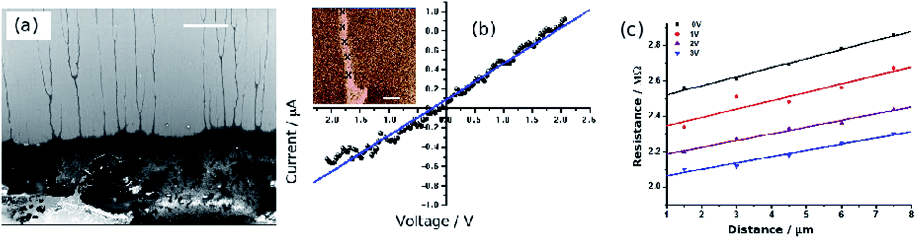 | ||
| Fig. 10 c-AFM measurements of Pd/DNA nanowires. (a) Electron micrograph of the dense mass of Pd/DNA nanowires (lower third of image); single Pd/DNA nanowires are seen protruding from the mass (scale bar = 20 μm). (b) Current–voltage curve with the tip contacting a single nanowire (inset = cAFM current image, data scale = 500 nA, tip/sample bias = 5 V, scale bar = 1 μm). (c) cAFM measurements of resistance at different points along a single Pd/DNA nanowire. The distance is that between the point at which the tip contacts the nanowire and the dense mass shown in (a) & (b). The nanowire resistance per unit length is the slope of the plot and the intercept at zero distance is the contact resistance. Measurements obtained at different setpoints (tip/sample force) are shown in different colours. Reprinted from ref. 55, Royal Society of Chemistry. | ||
3.3 Scanning conductance microscopy
The two-terminal device and the cAFM methods of assessing NW conductivity provide the most detailed information, but there is still a place for a rapid non-contact assessment of NW conductance. Scanned conductance microscopy (SCM) achieves this by mapping the phase shift in the tip motion as a metallised tip passes over a NW in lift mode. Lift mode is a two-pass technique in which a normal tapping scan is recorded in the first pass and in the second pass the tip retraces the topography of the sample at a chosen lift height above it. In this experiment the NW rests on a dielectric film, typically 200 nm SiO2 on Si, and a dc bias is applied between the tip and the underlying Si substrate. No dc current flows between the tip and substrate, but the energy stored in the tip/substrate capacitance adds to the mechanical energy in the cantilever and renormalises the spring constant. Near resonance the phase shift is proportional to the change in the spring constant and the square of the applied voltage. The change in the spring constant depends on the second derivative of the tip/substrate capacitance with respect to lift height and is therefore sensitive to objects in the tip/substrate gap. It has been shown that the phase shift Δϕ is always positive when a dielectric strip is present in the gap:62 | (6) |
R tip is the radius of the AFM tip, Q is the quality factor, k the spring constant, V the applied dc bias, h the lift height, t the (SiO2) dielectric thickness and εOx is the dielectric constant of the SiO2.
However, when the strip is a conductive nanowire (i.e., has free as opposed to bound charges in the usual sense of dielectric theory), then Rtip in the second term on the right hand side of eqn (6) should be replaced by a length L ≫ Rtip that corresponds to the length of the NW that is polarised on the experimental timescale. In the case of such a conductive NW, the phase shift will normally be negative. The method is surprisingly sensitive to NWs that are only weakly conductive because the NW/substrate capacitance is very small and therefore the NW may be fully polarized even if its resistance is rather large. In fact, one of the first uses of the method was to provide an upper bound on the conductivity of λ-DNA of order 10−16 Ω−1 cm−1.63 However, the method does not distinguish between two conductive NWs that are both polarized on the experimental timescale even if their resistances are different and is therefore not suited for quantitative comparisons of relatively highly conducting materials. The main advantages of the method are that it does not require any contacts to be prepared, it is straightforward to implement on many commercial AFMs and the ordinary tapping mode height image is obtained simultaneously with the SCM image.
Fig. 11 shows two examples. Fig. 11a is the height image of a Pd/DNA NW and Fig. 11b and c are phase images with bias voltages of +6 V and −6 V applied; the Pd/DNA NWs show up as conductive (thick darklines, negative phase shift) and it is possible to observe bare DNA molecules in Fig. 11a–c which indeed show up with a positive (white) phase shift indicating the absence of significant conductivity. For comparison, the AFM images of a Cu/DNA NW (Fig. 11d) and SCM (Fig. 11e) show that whilst it appears continuous, it is nevertheless insulating.
 | ||
| Fig. 11 Electrical characterisation of Pd/DNA nanowires by scanned conductance microscopy. (a) AFM height image of Pd/DNA nanowires (the data scale is 25 nm). (b) and (c) are the corresponding SCM phase images of the same nanowires with applied bias voltages of +6 V and 6 V respectively (the data scale is 3). The dark contrast indicates that the nanowires are conductive. Reprinted from ref. 55, Royal Society of Chemistry. (d) AFM image of a λ-DNA molecule subjected to treatment with Cu(CH3CN)4·PF6 and phenylsilane to produce a copper nanowire (inset: height profiles of copper nanostructure taken at various points along the structure) and (e) the corresponding EFM phase image at an applied bias of 10 V showing that the copper nanowire is insulating despite its continuous appearance. Scale bars = 500 nm. The colour scales of the images are (d) 20 nm and (e) 2.26 | ||
4 Conclusions
The initial stages of the formation of DNA-templated NWs is a nucleation and growth mechanism,12 which produces spherical particles on the template. Under the right conditions, this is followed by a transformation from this beads-on-a-string structure to a smooth, contiguous NW in a process that can be modelled by a coarse-grained linear thermodynamic treatment.56 This model makes two useful practical predictions: (i) the smooth NW is the equilibrium state as long as the amount of templated material does not exceed a threshold that depends on the surface tension of the material and its adhesion to the template (2) and (ii) the transformation to the final equilibrium state is usually much slower than the initial deposition of material on the template and sufficient time must be allowed for this to occur.After chemical and structural characterisation, the most crucial measurement to make on the NW is that of its electrical conductivity. For a simple pass/fail assessment of NWs, scanned conductance microscopy is the most convenient and may be carried out at the same time as characterisation by AFM. Deeper studies of the conduction process require either conductive AFM (cAFM) or photolithographically-defined microelectrodes. cAFM experiments can take advantage of the fact that DNA-templated NWs are often formed as an aqueous suspension; a dried droplet of the suspension leaves individual NWs protruding from the main mass and greatly facilitates the preparation of a contact. These experiments allow a straightforward estimate of the contact resistances and the actual NW conductivity through the use of the closed-loop positioning of the AFM to move the tip along an individual NW whilst taking current–voltage measurements. Finally, the temperature-dependence of conductivity, which is crucial for an assessment of the conduction mechanism, is best performed with microfabricated electrodes to contact the NW directly so that a conventional probe-station can be used to measure current–voltage curves under controlled atmosphere and temperature. We find that embedding the electrodes into a thick oxide layer on the device, so that there is a minimal change in height at the dielectric/electrode boundary, simplifies the task of alignment of the NWs across the electrode gap by molecular combing.
Abbreviations
| X/DNA indicates | X templated on DNA |
| NW | Nanowire |
| NP | Nanoparticle |
| TMSCl | Trimethylsilylchloride |
| AFM | Atomic force microscopy |
| cAFM | Conductive atomic force microscopy |
| SCM | Scanned conductance microscopy |
| TEM | Transmission electron microscopy |
Acknowledgements
The EU FP7 and Marie Curie Fellowship programs are thanked for funding parts of this work through the LAMAND and NANOEMBRACE projects. ONE and Intel are thanked for funding research at Newcastle in conductive nanowires.References
-
G. M. Blackburn and M. J. Gait, Nucleic Acids in Chemistry and Biology, OUP, Oxford, 2nd edn, 1996 Search PubMed
.
- Y. Ma, J. Zhang, G. Zhang and H. He, J. Am. Chem. Soc., 2004, 126, 7097–7101 CrossRef CAS PubMed
- P. Nickels, W. U. Dittmer, S. Beyer, J. P. Kotthaus and F. C. Simmel, Nanotechnology, 2004, 15, 1524–1529 CrossRef CAS
- L. Dong, T. Hollis, S. Fishwick, B. A. Connolly, N. G. Wright, B. R. Horrocks and A. Houlton, Chem. – Eur. J., 2007, 13, 822–828 CrossRef CAS PubMed
- J. Bednar, P. Furrer, V. Katritch, A. Stasiak, J. Dubochet and A. Stasiak, J. Mol. Biol., 1995, 254, 579–594 CrossRef CAS
- J. Westwater, D. P. Gosain, S. Tomiya, S. Usui and H. Ruda, J. Vac. Sci. Technol., B: Microelectron. Nanometer Struct., 1997, 15, 554–557 CrossRef CAS
- L. Dong, T. Hollis, B. A. Connolly, N. G. Wright, B. R. Horrocks and A. Houlton, Adv. Mater., 2007, 19, 1748–1751 CrossRef CAS
- E. Braun and K. Keren, Adv. Phys., 2004, 53, 441–496 CrossRef CAS
- R. M. Stoltenberg and A. T. Woolley, Biomed. Microdevices, 2004, 6, 105–111 CrossRef CAS
- A. Houlton, A. R. Pike, M. A. Galindo and B. R. Horrocks, Chem. Commun., 2009, 1797–1806 RSC
- S. M. D. Watson and A. Houlton, Annu. Rep. Prog. Chem., Sect. A: Inorg. Chem., 2011, 107, 21–42 RSC
- E. Braun, Y. Eichen, U. Sivan and G. Ben-Yoseph, Nature, 1998, 391, 775–778 CrossRef CAS PubMed
- H. A. Becerril, R. M. Stolenberg, D. R. Wheeler, R. C. Davis, J. N. Harb and A. T. Woolley, J. Am. Chem. Soc., 2005, 127, 2828–2829 CrossRef CAS PubMed
- H. Yan, S. H. Park, G. Finkelstein, J. H. Reif and T. H. LaBean, Science, 2003, 301, 1882–1884 CrossRef CAS PubMed
- K. Keren, R. S. Berman and E. Braun, Nano Lett., 2004, 4, 323–326 CrossRef CAS
- G. A. Burley, J. Gierlich, M. R. Mofid, H. Nir, S. Tal, Y. Eichen and T. Carell, J. Am. Chem. Soc., 2006, 128, 1398–1399 CrossRef CAS PubMed
- M. Fischler, U. Simon, H. Nir, Y. Eichen, G. A. Burley, J. Gierlich, P. M. E. Gramlich and T. Carell, Small, 2007, 3, 1049–1055 CrossRef CAS PubMed
- M. Mertig, L. C. Ciacchi, R. Seidel, W. Pompe and A. De Vita, Nano Lett., 2002, 2, 841–844 CrossRef CAS
- C. F. Monson and A. T. Woolley, Nano Lett., 2003, 3, 359–363 CrossRef CAS
- S. M. D. Watson, N. G. Wright, B. R. Horrocks and A. Houlton, Langmuir, 2010, 26, 2068–2075 CrossRef CAS PubMed
- H. A. Becerril, P. Ludtke, B. M. Willardson and A. T. Woolley, Langmuir, 2006, 22, 10140–10144 CrossRef CAS PubMed
- S. M. D. Watson, H. D. A. Mohamed, B. R. Horrocks and A. Houlton, Nanoscale, 2013, 5, 5349–5359 RSC
- Q. Gu and D. T. Haynie, Mater. Lett., 2008, 62, 3047–3050 CrossRef CAS PubMed
- J. Richter, R. Seidel, R. Kirsch, M. Mertig, W. Pompe, J. Plaschke and H. K. Schackert, Adv. Mater., 2000, 12, 507–510 CrossRef CAS
- J. Richter, M. Mertig, W. Pompe, I. Monch and H. K. Schackert, Appl. Phys. Lett., 2001, 78, 536–538 CrossRef CAS PubMed
-
J. Pate, Fabrication and Characterisation of DNA-templated Copper Nanowires, PhD thesis, Newcastle University, UK, 2013
- H. J. Kim, Y. Roh and B. Hong, IEEE Trans. Nanotechnol., 2010, 9, 254–257 CrossRef
- H. Cho, S. K. Kim, Y. Jung, J. Jung and B. H. Chung, Chem. Commun., 2011, 47, 5756–5758 RSC
- W. E. Ford, O. Harnack, A. Yasuda and J. M. Wessels, Adv. Mater., 2001, 13, 1793–1797 CrossRef CAS
- Q. Gu, H. Jin and K. Dai, J. Phys. D: Appl. Phys., 2009, 42, 015303 CrossRef
- Q. Gu, C. Cheng, S. Suryanarayanan, K. Dai and D. T. Haynie, Phys. E, 2006, 33, 92–98 CrossRef CAS PubMed
- H. Kudo and M. Fujihara, IEEE Trans. Nanotechnol., 2006, 5, 90–92 CrossRef
- J. Liu, Y. Geng, E. Pound, S. Gyawali, J. R. Ashton, J. Hickey, A. T. Woolley and J. N. Harb, ACS Nano, 2011, 5, 2240–2247 CrossRef CAS PubMed
- J. L. Coffer, S. R. Bigham, R. F. Pinizzotto and H. Yang, Nanotechnology, 1992, 3, 69–76 CrossRef
- M. Achermann, S. Jeong, L. Balet, G. A. Montano and J. A. Hollingsworth, ACS Nano, 2011, 5, 1761–1768 CrossRef CAS PubMed
- J. Su, F. Gao and L. Hou, Mater. Lett., 2013, 92, 206–209 CrossRef CAS PubMed
- W. U. Dittmer and F. C. Simmel, Appl. Phys. Lett., 2004, 85, 633–635 CrossRef CAS PubMed
- L. Levina, W. Sukhovatkin, S. Musikhin, S. Cauchi, R. Nisman, D. P. Bazett-Jones and E. H. Sargent, Adv. Mater., 2005, 17, 1854–1857 CrossRef CAS
- H. D. A. Mohamed, S. M. D. Watson, B. R. Horrocks and A. Houlton, Nanoscale, 2012, 4, 5936–5945 RSC
- P. W. Bauwmeister, Phys. Rev., 1961, 121, 359–362 CrossRef
- M. Fujinaka and A. A. Berezin, J. Appl. Phys., 1983, 54, 3582–3588 CrossRef CAS PubMed
- R. Hassanien, S. A. Farha Al-Said, L. Šiller, R. Little, N. G. Wright, A. Houlton and B. R. Horrocks, Nanotechnology, 2012, 23, 075601 CrossRef PubMed
- J. Liu, B. Uprety, S. Gyawali, A. T. Woolley, N. V. Myung and J. N. Harb, Langmuir, 2013, 29, 11176–11184 CrossRef CAS PubMed
- S. N. Sarangi, S. Rath, K. Goswami, S. Nozaki and S. N. Sahu, Phys. E, 2010, 42, 1670–1674 CrossRef CAS PubMed
- S. Pu, A. Zinchenko and S. Murata, Nanotechnology, 2011, 22, 375604 CrossRef PubMed
- S. M. D. Watson, J. H. Hedley, M. A. Galindo, S. A. Farha Al-Said, N. G. Wright, B. A. Connolly, B. R. Horrocks and A. Houlton, Chem. – Eur. J., 2012, 18, 12008–12019 CrossRef CAS PubMed
- R. Hassanien, M. Al-Hinai, S. A. Farha Al-Said, R. Little, L. Šiller, N. G. Wright, A. Houlton and B. R. Horrocks, ACS Nano, 2010, 4, 2149–2159 CrossRef CAS PubMed
- S. A. F. Al-Said, R. Hassanien, J. Hannant, M. A. Galindo, S. Pruneanu, A. R. Pike, A. Houlton and B. R. Horrocks, Electrochem. Commun., 2009, 11, 550–553 CrossRef PubMed
- J. Hannant, J. H. Hedley, J. Pate, A. Walli, S. A. Farha Al-Said, M. A. Galindo, B. A. Connolly, B. R. Horrocks, A. Houlton and A. R. Pike, Chem. Commun., 2010, 46, 5870–5872 RSC
- K. Sugikawa, K. Kaneko, K. Sada and S. Shinkai, Langmuir, 2010, 26, 19100–19105 CrossRef CAS PubMed
- D. Bensimon, A. J. Simon, V. Croquette and A. Bensimon, Phys. Rev. Lett., 1995, 74, 4754–4757 CrossRef CAS
- S. Pruneanu, S. A. F. Al-Said, L. Q. Dong, T. Hollis, M. A. Galindo, N. G. Wright, A. Houlton and B. R. Horrocks, Adv. Funct. Mater., 2008, 18, 2444–2454 CrossRef CAS
- C. R. Martin, Science, 1994, 266, 1961–1966 CAS
- A. M. Morales and C. M. Lieber, Science, 1998, 279, 208–210 CrossRef CAS
- M. N. Al-Hinai, R. Hassanien, N. G. Wright, A. B. Horsfall, A. Houlton and B. R. Horrocks, Faraday Discuss. Chem. Soc., 2013, 164, 71–91 RSC
- S. M. D. Watson, A. Houlton and B. R. Horrocks, Nanotechnology, 2012, 23, 505603 CrossRef PubMed
- D. E. Wolf and J. Villain, Europhys. Lett., 1990, 13, 389–394 CrossRef CAS
- S. M. D. Watson, M. A. Galindo, B. R. Horrocks and A. Houlton, Mechanism of formation of supramolecular DNA-templated nanowires, manuscript under review.
- A. S. Walton, C. S. Allen, K. Critchley, M. L. Górzny, J. E. McKendry, R. M. D. Brydson, B. J. Hickey and S. D. Evans, Nanotechnology, 2007, 18, 065204 CrossRef
- C. Hermosa, J. V. Álvarez, M.-R. Azani, C. J. Gómez-García, M. Fritz, J. M. Soler, J. Gómez-Herrero, C. Gómez-Navarro and F. Zamora, Nat. Commun., 2013, 4, 1709 CrossRef PubMed
- M. Wnek, M. L. Górzny, M. B. Ward, C. Wälti, A. G. Davies, R. Brydson, S. D. Evans and P. G. Stockley, Nanotechnology, 2013, 24, 025605 CrossRef CAS PubMed
- C. Staii, A. T. Johnson and N. J. Pinto, Nano Lett., 2004, 4, 859–962 CrossRef CAS
- M. Bockrath, N. Markovic, A. Shepard, M. Tinkham, L. Gurevich, L. P. Kouwenhoven, M. W. Wu and L. L. Sohn, Nano Lett., 2002, 2, 187–190 CrossRef CAS
| This journal is © The Royal Society of Chemistry 2014 |