
 Open Access Article
 This Open Access Article is licensed under a
 Creative Commons Attribution 3.0 Unported Licence
Fabrication of semi-transparent perovskite films with centimeter-scale superior uniformity by the hybrid deposition method†
Luis K.
Ono‡
,
Shenghao
Wang‡
,
Yuichi
Kato
,
Sonia R.
Raga
and
Yabing
Qi
*
Energy Materials and Surface Sciences Unit, Okinawa Institute of Science and Technology Graduate University, 1919-1 Tancha Onna-son, Okinawa 904-0495, Japan. E-mail: yabing.qi@oist; Fax: +81 098-966-1062; Tel: +81 098-966-8435
First published on 4th September 2014
Abstract
We report the development of instrumentation and methodology for fabricating large area semi-transparent organo-lead-halide perovskite films. In our method, the growth of perovskite films relies on the control of CH3NH3I flow and vapor pressure inside a vacuum chamber. Solar cell devices based on the prepared semi-transparent perovskite films as thin as ∼135 nm achieved an efficiency of 9.9% and a high open circuit voltage of 1.09 V.
Broader contextCurrently, crystalline Si solar cells represent the dominant photovoltaic technology. The highest efficiency for these kinds of cells is around 28%, but the overall cost to use these solar cells as an energy source is still significantly higher than conventional energy supplies (e.g., fossil fuels). Organometal halide perovskite (OHP) solar cells have emerged as the most promising candidates for the next generation high efficiency solar cell technology that is compatible with low cost and large-area fabrication. There is plenty of room for further improvements. In particular, the development of protocols to make such a technology practical and applicable to industry is of paramount importance. In this work, we report on the development of instrumentation and methodology for depositing semi-transparent OHP films with centimeter-scale superior uniformity (5 × 5 cm2), good crystallinity and high reproducibility, which is particularly suitable for large-area applications such as window photovoltaics. High-performance solar cell devices (Jsc = 17 mA cm−2, Voc = 1.09 V, PCE = 9.9%) were obtained using our methodology, which further testifies its potential. |
It has been demonstrated that organo-lead-halide perovskite (OHP) based solar cells can achieve solar energy-to-electricity power conversion efficiency (PCE) as high as 16.2% and are compatible with protocols for low-cost solar cell fabrication.1–6 The nature of the OHP materials to form long-range ordering in their crystal structure, abundance, inexpensive as raw materials, and the easy processability at 150 °C temperature (solution and vacuum evaporation) are major advantages for photovoltaic applications.7–10 However, very few reports were documented regarding the scaling up of such solar cells although it is widely acknowledged that the methodologies for large area fabrication have to be developed to make a photovoltaic technology viable. Generally, large area processing is challenging due to vast variation in the film thickness, rough film morphology, and uncontrolled stoichiometry and crystallinity changes across the substrate area.
The film thickness, morphology, stoichiometry, crystallinity as well as material purity have a significant impact on the overall solar cell performance.7,11,12 A variety of deposition techniques have been reported including one-step spin-coating,10,13–17 two-step deposition techniques,12,18,19 vapor-assisted solution processes,20 and vacuum deposition.8,21,22 One-step spin-coating is the most widely used method to prepare the solar cells due to its simplicity and low-cost. However, the films prepared by this method have been reported to have a poor morphology.7,13 In the two-step process, a layer of metal halide is deposited by spin-coating followed by dipping the film into the organic salt solution and perovskite formed by a chemical reaction. However, due to high reaction rates of the perovskite formation, it is challenging to optimize the processing conditions with sufficient reproducibility. To circumvent these issues, the incorporation of CH3NH3I (MAI) into the spin-coated PbI2 film via vapor (the so-called vapor-assisted solution process) has been proposed to generate high quality films with a PCE of 12.1%.20 On the other hand, neither the two-step process nor the vapor-assisted solution process can be applied to metal halides with poor solubility (e.g., PbCl2). Vacuum evaporation techniques have also been employed using standard dual-source physical deposition processes. This technique enables better control of the film thickness and morphology. However, a number of factors such as simultaneous control of the evaporation rates of the PbCl2 and MAI sources that have significantly different vapor,23 non-uniform film composition if ratios of PbCl2 and MAI evaporation rates are not well controlled, limited area with lateral composition uniformity, and high consumption of MAI present challenges for this technique to be widely applied for large scale fabrication.8,21,22
In this work, we describe home-built instrumentation that is capable to generate perovskite films with centimeter-scale superior uniformity (5 × 5 cm2), good crystallinity and high reproducibility. For simplicity, in the rest of the letter, we will use MAI and PbCl2 as the example material system. On the other hand, it should be noted that this method has been tested to be of general use for other combinations of MA halides and Pb halides. The working principle of our system relies on controlling the MAI vapor partial pressure inside the vacuum chamber that is monitored by a QCM facing the opposite side of the MAI evaporator source (upwards, Part #7 in Fig. 1a). The second QCM that is facing the PbCl2 evaporator source (downwards, Part #6 in Fig. 1a) helps to determine the total rate of PbCl2 and MAI. Only when the MAI vapor is generated, the QCM that faces upwards starts to detect a rate, which confirms that the MAI is largely vapor-induced, i.e., non-directional. Our hybrid deposition method provides good control on the nominal stoichiometry of MAI and PbCl2. In comparison, in the solution method, the solubility of reactants in solvents is an additional parameter that needs to be considered. For example, it is observed that it is difficult to dissolve PbCl2 in N,N-dimethylformamide when the MAI–PbCl2 molar ratio is lower than 3![[thin space (1/6-em)]](https://www.rsc.org/images/entities/char_2009.gif) :1.24 In this sense, our hybrid deposition method is advantageous because the ratio of the two reactants (i.e. lead halide and MAI) can be tuned in a wider range under vapor evaporation conditions and therefore it is not limited by solubility. Devices based on ultra-thin perovskite films of ∼50 nm prepared by our hybrid deposition method without the post-annealing procedure achieved a PCE of 6.3% with an open-circuit voltage (Voc) of 1.06 V. These ultra-thin perovskite films showed a high degree of crystallinity, a smooth surface, and a semi-transparent color that meet the requisites for window photovoltaic applications.25,26
:1.24 In this sense, our hybrid deposition method is advantageous because the ratio of the two reactants (i.e. lead halide and MAI) can be tuned in a wider range under vapor evaporation conditions and therefore it is not limited by solubility. Devices based on ultra-thin perovskite films of ∼50 nm prepared by our hybrid deposition method without the post-annealing procedure achieved a PCE of 6.3% with an open-circuit voltage (Voc) of 1.06 V. These ultra-thin perovskite films showed a high degree of crystallinity, a smooth surface, and a semi-transparent color that meet the requisites for window photovoltaic applications.25,26
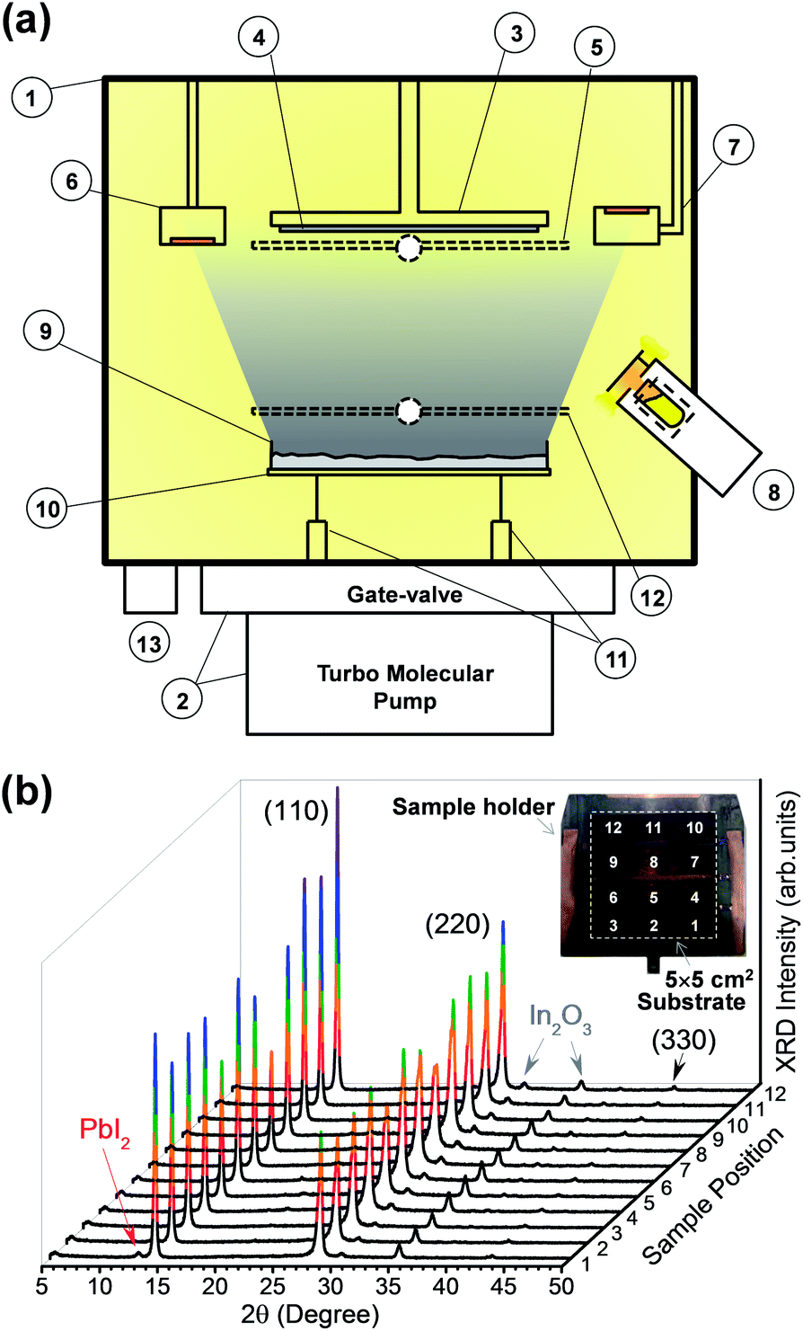 | ||
| Fig. 1 (a) Side view of the hybrid deposition method system: (1) main vacuum chamber; (2) pumping system comprising a gate-valve and a turbo molecular pump; (3) substrate holder stage which allows cooling and heating from −190 °C to 200 °C; (4) substrate sizes of up to 5 × 5 cm2; (5) substrate shutter; (6) QCM facing downwards; (7) QCM facing upwards; (8) Knudsen cell evaporator for producing MAI vapor partial pressure; (9) widely opened dish-shaped crucible for the evaporation of lead halide compounds; (10) spiral-shaped tungsten wire; (11) electric feedthroughs; (12) lead halide shutter; (13) pressure gauge. (b) XRD and picture of the perovskite film prepared in the hybrid deposition system on a large (5 × 5 cm2) ITO/glass substrate and measured at 12 different points. Note that the as-prepared films show a light-orange color. The dark brown color in the picture is from the copper sample holder. | ||
The overall design of the system is shown in Fig. 1a and S1.† The detailed descriptions of the components comprising the hybrid deposition method system as well as the protocols for the evaporation rate calibrations (Fig. S2†) and fabrication of perovskite films can be found in the Experimental section (ESI†). The macroscopic uniformity of perovskite films prepared in our system was evaluated by evaporating a film of ∼135 nm thickness on tin-doped indium oxide (ITO)/glass with a substrate area of 5 × 5 cm2 (Fig. 1b). A picture of the as-prepared film (inset in Fig. 1b) shows a uniform semi-transparent light-orange color across the entire substrate area. XRD was measured at 12 different points showing everywhere similar intensities of the characteristic diffraction peaks at 14.0°, 28.4°, and 43.1° corresponding to the (110), (220), and (330) planes of CH3NH3PbI3−xClx. Additional diffraction peaks corresponding to the ITO substrate as well as PbI2 were also detected. The small PbI2 peak is most likely caused by the ambient exposure of the perovskite film while the 12 spot ex situ XRD measurements were performed.27,28 Both the crystalline uniformity and the thickness variation over the 5 × 5 cm2 area were investigated. As shown in Fig. S3,† AFM measurements were conducted on a batch of samples to investigate the film thickness variation over the 5 × 5 cm2 area. Two measurements, one conducted at the center of the sample (Fig. S3b†) and another at one edge (Fig. S3c†) showed a film thickness variation of 2%. Based on our AFM analysis, our perovskite films showed to be extremely uniform in the length scale of micro-meter (Fig. 2b) without clear crystallite domain structures, which is drastically different from the solution processed perovskite films. This is in agreement with the observations by Liu et al.21
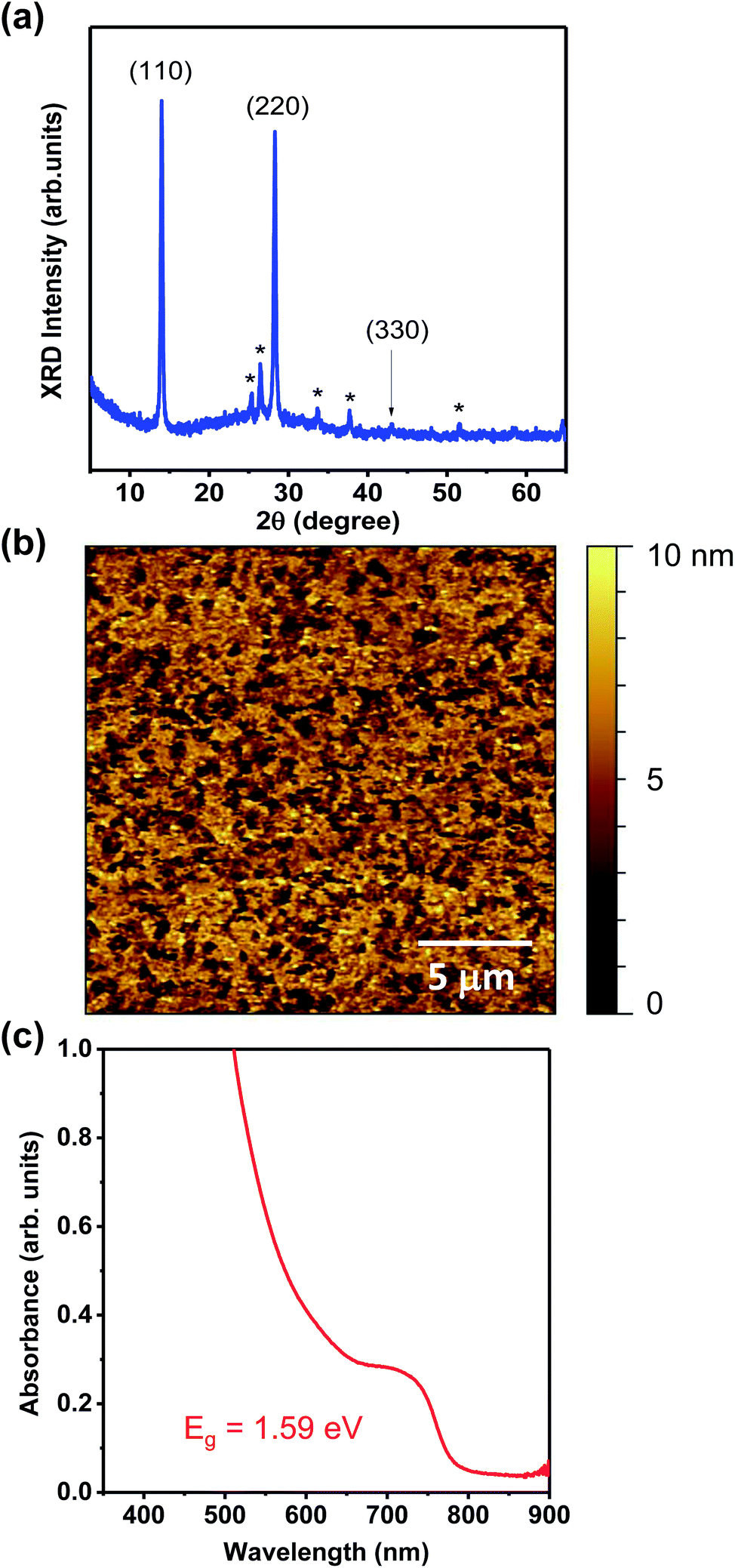 | ||
| Fig. 2 (a) XRD data of the ∼50 nm thick perovskite film reveal the characteristic peaks at 14.0°, 28.4°, and 43.1° corresponding to (110), (220), and (330) in CH3NH3PbI3−xClx. Additional peaks labeled with * correspond to the FTO substrate. (b) AFM topography image (scan size: 20 μm × 20 μm) of the perovskite film deposited on the ITO substrate from which the surface RMS roughness of ∼4.6 nm was extracted. (c) Optical absorption on the ∼135 nm perovskite film showing a sharp rise at 780 nm corresponding to a bandgap of 1.59 eV. | ||
After optimizing the conditions in our system by tuning the evaporation rates of MAI and PbCl2, perovskite films of two different thicknesses (∼50 nm and ∼135 nm) were grown. XRD measurements of the ∼50 nm thick perovskite film (Fig. 2a) revealed the characteristic diffraction peaks of (110), (220), and (330) planes of CH3NH3PbI3−xClx usually assigned to the orthorhombic crystal structure.21 Looking closely at the (220) diffraction peak, no characteristic feature of a double-peak was observed that is indicative of CH3NH3PbI3 phase formation.8,29 The absence of the peak at 15.7° (the characteristic peak for the CH3NH3PbCl3 phase) and the detection of the (330) peak confirmed the high phase-purity and crystallinity of our perovskite films. In addition, the (110) peak is stronger than (220) even without the post-annealing treatments which is a common procedure employed after the film growth.20,21 The macroscopic and microscopic uniformities of perovskite films were confirmed by optical microscopy (Fig. S4†) and AFM topography (Fig. 2b), respectively. The as-prepared samples with ∼50 nm and ∼135 nm perovskite films showed a uniform semi-transparent light-orange color, which was distinctively different from the black or dark brownish color commonly observed in solution processed samples. Based on AFM measurements on a 20 μm × 20 μm sample area, these ∼50 nm and ∼135 nm perovskite films had a root-mean square (RMS) surface roughness as low as ∼4.6 nm and ∼9 nm when deposited on flat substrates, respectively, corresponding to their intrinsic film roughness (Fig. 2b). When rougher substrates of compact TiO2/FTO were used, the perovskite films were conformal to the top compact TiO2 showing a surface roughness of ∼30 nm which corresponded to the same roughness of compact TiO2/FTO. In comparison, the solution-processed perovskite films following the procedure in ref. 7 were extremely rough as measured by AFM (not shown) with a RMS roughness of ∼243 nm (scan size 20 μm × 20 μm). The UV-vis acquired on the thicker perovskite film (∼135 nm) showed a sharp rise at 780 nm corresponding to a bandgap of 1.59 eV in good agreement with previous reports.29,30 The best performing device for the ∼50 nm perovskite film (Fig. 3a, blue curve) under standard AM1.5G illumination achieved a short-circuit photocurrent (Jsc) of 10.5 mA/cm2, a Voc of 1.06 V, a fill factor (FF) of 0.566, and 6.3% power-conversion efficiency (PCE). On the thicker perovskite film (∼135 nm), the measured J–V curve under standard AM1.5G illumination produced Jsc, Voc, FF, and PCE of 17 mA/cm2, 1.09 V, 0.535, and 9.9%, respectively (Fig. 3a, red curve). The average and standard deviation values of 9.5 ± 0.9 mA/cm2 (16.2 ± 0.6 mA/cm2), 0.98 ± 0.10 V (1.06 ± 0.05 V), 0.500 ± 0.007 (0.490 ± 0.003), and 4.7 ± 1.2% (8.45 ± 1.03%) were extracted based on a batch of sample with 6 cells on the perovskite films with ∼50 nm (and ∼135 nm). All devices showed similar J–V characteristics (Fig. S5†), which exemplifies the superior uniformity of the perovskite films prepared using our system and method. The high performance of these solar cell devices is a strong indication that our new instrumentation and methodology can be employed to fabricate state-of-the-art photovoltaic products. The high Voc (over 1 V) typically achieved by our devices with ∼50 nm and ∼135 nm perovskite films well aligns with the reported values using vapor deposition methods: 1.07 V in the work of Liu et al.21 and 1.05 V in the work of Malinkiewicz et al.8 On the other hand, solution processed ones have generally substantially lower Voc possibly because of large variations of the film thickness.21Voc depends on various factors, one of which is the recombination processes (or charge life-time) present at the interfaces of different layers within a perovskite-based solar cell as well as within each layer.31–33 Uniform layer perovskite formation prevents the shunting pathways effectively, leading to a lower recombination rate. In addition, it has been proposed that perovskites are ionic materials that have the property to generate only shallow trap states.31–33 Therefore, perovskite solar cell performance is expected to be only weakly dependent on grain sizes. This is consistent with the observations that perovskite solar cells show a similar level of high efficiencies although they are prepared by different methods (e.g. solution processing or vacuum evaporation). In general, vacuum prepared perovskites show lower XRD peak intensities than the films prepared by the solution processing method.8,21,34 More interestingly, the intensities of the XRD peaks seem to do not correlate directly with the high performance of solar cells.21,34–36 The XRD data by Barrows et al.35 show additional peaks for the (110), (220), and (330) planes of tetragonal MAPbI3−xClx and are assigned to the excess PbCl2. However, a performance of 11.1% was obtained for their champion cell with 330 nm perovskite thickness. Similarly, the presence of excess PbI2 has been also shown to have beneficial effects on the solar cell performance showing PCE as high as 12%.36 The magnitude of the hysteresis effects in our cells was characterized by sweeping the applied voltage from −0.2 V to +1.1 V (reverse). Significant hysteresis of the J–V scans was observed (Fig. S6†) for our perovskite solar cells and a PCE decrease of ∼30% was observed on the reverse bias. The exact cause for the hysteresis features is not clear to us at the moment and this topic is still under investigation in our group. The external quantum efficiency (EQE), or incident-photon-to-current conversion efficiency, spectra of the complete devices illuminated under monochromatic light (Fig. 3b) show the generation of photocurrent starting from ∼780 nm in agreement with the band-gap of CH3NH3PbI3−xClx determined by UV-vis (Fig. 2c). Our solar cells with ∼50 nm and ∼135 nm perovskite layers reach ∼45% and ∼80%, respectively, in the range of 420–510 nm. A decrease in EQE intensity is observed in the 500–750 nm range which might be induced by the presence of small concentrations of Cl (below 3–4%).29 In contrast, the pure phase CH3NH3PbI3 films were reported to produce a high EQE of ∼70–80% over a long wavelength range of 350–750 nm.20 However, the beneficial effects of the presence of the two different halogens (I and Cl) within the crystalline structure for obtaining high conductivity have been demonstrated.29
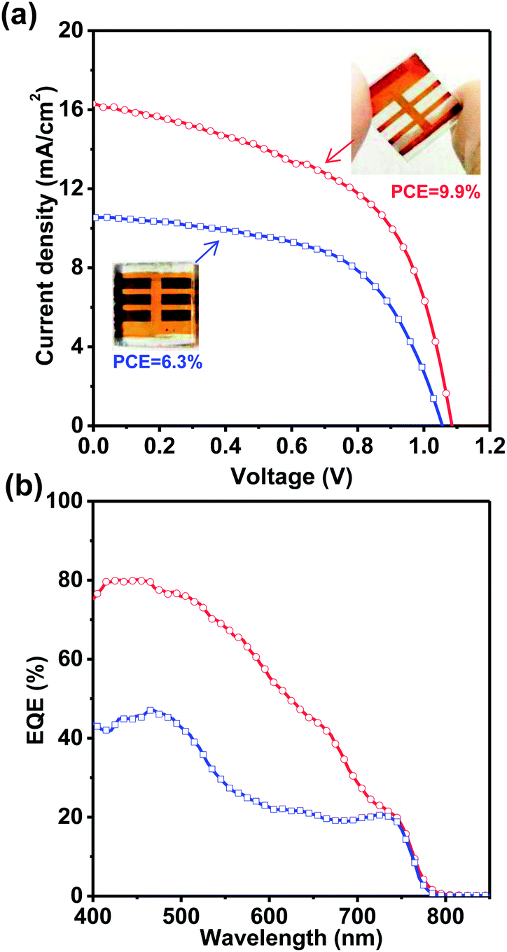 | ||
| Fig. 3 (a) Current density–voltage (J–V) characteristics of the solar cells based on the perovskite films with two different thicknesses prepared by the hybrid deposition method under AM 1.5G illumination. Solar energy-to-electricity conversions of 6.3% (blue curve) and 9.9% (red curve) were extracted for devices using ∼50 nm and ∼135 nm perovskite films, respectively. (b) Corresponding external quantum efficiency spectra. The inset in (a) shows pictures of the actual devices showing a semi-transparent light-orange color. | ||
We have demonstrated that perovskite films as thin as ∼135 nm can generate a PCE of 9.9% when implemented in solar cells by controlling the PbCl2 evaporation rate and MAI vapor pressure in our hybrid deposition method. Such a perovskite film growth method provides a centimeter-scale uniform semi-transparent color that is particularly suitable for large-scale window photovoltaic applications25,26 where good transparency is a prerequisite. In addition, although in this article, we have focused on the particular case of using the PbCl2 and MAI powders for the generation of CH3NH3PbI3−xClx perovskite films, our hybrid evaporation method can be easily adopted for the evaporation of other lead halides such as PbI2 and PbBr2 or their combinations. Such mixed-halide perovskite films with different compositions were reported to allow bandgap tunability properties,28,37 thus, providing flexibility on perovskite film color choices as well as suitability for the development of perovskite-based tandem solar cells.
Acknowledgements
This work was financially supported by Okinawa Institute of Science and Technology Graduate University in Japan. We thank Professor David Cahen and Dr. Saar Kirmayer from Weizmann Institute of Science in Israel for providing MAI for some initial tests.Notes and references
- A. Kojima, K. Teshima, Y. Shirai and T. Miyasaka, J. Am. Chem. Soc., 2009, 131, 6050–6051 CrossRef CAS PubMed
.
- H. J. Snaith, J. Phys. Chem. Lett., 2013, 4, 3623–3630 CrossRef CAS
- G. Hodes and D. Cahen, Nat. Photonics, 2014, 8, 87–88 CrossRef CAS
- M. He, D. J. Zheng, M. Y. Wang, C. J. Lin and Z. Q. Lin, J. Mater. Chem. A, 2014, 2, 5994–6003 CAS
- H. S. Kim, S. H. Im and N. G. Park, J. Phys. Chem. C, 2014, 118, 5615–5625 CAS
- S. Kazim, M. K. Nazeeruddin, M. Grätzel and S. Ahmad, Angew. Chem., Int. Ed., 2014, 53, 2812–2824 CrossRef CAS PubMed
- A. Dualeh, N. Tétreault, T. Moehl, P. Gao, M. K. Nazeeruddin and M. Grätzel, Adv. Funct. Mater., 2014, 24, 3250–3258 CrossRef CAS
- O. Malinkiewicz, A. Yella, Y. H. Lee, G. M. Espallargas, M. Graetzel, M. K. Nazeeruddin and H. J. Bolink, Nat. Photonics, 2014, 8, 128–132 CrossRef CAS
- C. Roldan-Carmona, O. Malinkiewicz, A. Soriano, G. M. Espallargas, A. Garcia, P. Reinecke, T. Kroyer, M. I. Dar, M. K. Nazeeruddin and H. J. Bolink, Energy Environ. Sci., 2014, 7, 994–997 CAS
- K. Wojciechowski, M. Saliba, T. Leijtens, A. Abate and H. J. Snaith, Energy Environ. Sci., 2014, 7, 1142–1147 CAS
- G. E. Eperon, V. M. Burlakov, P. Docampo, A. Goriely and H. J. Snaith, Adv. Funct. Mater., 2014, 24, 151–157 CrossRef CAS
- J. Burschka, N. Pellet, S. J. Moon, R. Humphry-Baker, P. Gao, M. K. Nazeeruddin and M. Gratzel, Nature, 2013, 499, 316–319 CrossRef CAS PubMed
- B. Conings, L. Baeten, C. De Dobbelaere, J. D'Haen, J. Manca and H. G. Boyen, Adv. Mater., 2014, 26, 2041–2046 CrossRef CAS PubMed
- B. Cai, Y. D. Xing, Z. Yang, W. H. Zhang and J. S. Qiu, Energy Environ. Sci., 2013, 6, 1480–1485 CAS
- H. S. Kim, C. R. Lee, J. H. Im, K. B. Lee, T. Moehl, A. Marchioro, S. J. Moon, R. Humphry-Baker, J. H. Yum, J. E. Moser, M. Gratzel and N. G. Park, Sci. Rep., 2012, 2, 591 Search PubMed
- E. Edri, S. Kirmayer, D. Cahen and G. Hodes, J. Phys. Chem. Lett., 2013, 4, 897–902 CrossRef CAS
- J. T. W. Wang, J. M. Ball, E. M. Barea, A. Abate, J. A. Alexander-Webber, J. Huang, M. Saliba, I. Mora-Sero, J. Bisquert, H. J. Snaith and R. J. Nicholas, Nano Lett., 2014, 14, 724–730 CrossRef CAS PubMed
- K. N. Liang, D. B. Mitzi and M. T. Prikas, Chem. Mater., 1998, 10, 403–411 CrossRef CAS
- D. Q. Bi, S. J. Moon, L. Haggman, G. Boschloo, L. Yang, E. M. J. Johansson, M. K. Nazeeruddin, M. Gratzel and A. Hagfeldt, RSC Adv., 2013, 3, 18762–18766 RSC
- Q. Chen, H. Zhou, Z. Hong, S. Luo, H.-S. Duan, H.-H. Wang, Y. Liu, G. Li and Y. Yang, J. Am. Chem. Soc., 2013, 136, 622–625 CrossRef PubMed
- M. Z. Liu, M. B. Johnston and H. J. Snaith, Nature, 2013, 501, 395–398 CrossRef CAS PubMed
- A. S. Subbiah, A. Halder, S. Ghosh, N. Mahuli, G. Hodes and S. K. Sarkar, J. Phys. Chem. Lett., 2014, 5, 1748–1753 CrossRef CAS
- S. T. Ha, X. Liu, Q. Zhang, D. Giovanni, T. C. Sum and Q. Xiong, Adv. Opt. Mater., 2014, 2, 838–844 CAS
- M. M. Lee, J. Teuscher, T. Miyasaka, T. N. Murakami and H. J. Snaith, Science, 2012, 338, 643–647 CrossRef CAS PubMed
- R. F. Service, Science, 2014, 344, 458 CrossRef PubMed
- G. E. Eperon, V. M. Burlakov, A. Goriely and H. J. Snaith, ACS Nano, 2014, 8, 591–598 CrossRef CAS PubMed
- G. D. Niu, W. Z. Li, F. Q. Meng, L. D. Wang, H. P. Dong and Y. Qiu, J. Mater. Chem. A, 2014, 2, 705–710 CAS
- J. H. Noh, S. H. Im, J. H. Heo, T. N. Mandal and S. I. Seok, Nano Lett., 2013, 13, 1764–1769 CAS
- S. Colella, E. Mosconi, P. Fedeli, A. Listorti, F. Gazza, F. Orlandi, P. Ferro, T. Besagni, A. Rizzo, G. Calestani, G. Gigli, F. De Angelis and R. Mosca, Chem. Mater., 2013, 25, 4613–4618 CrossRef CAS
- P. Schulz, E. Edri, S. Kirmayer, G. Hodes, D. Cahen and A. Kahn, Energy Environ. Sci., 2014, 7, 1377–1381 CAS
- R. S. Sanchez, V. Gonzalez-Pedro, J.-W. Lee, N.-G. Park, Y. S. Kang, I. Mora-Sero and J. Bisquert, J. Phys. Chem. Lett., 2014, 5, 2357–2363 CrossRef CAS
- V. Gonzalez-Pedro, E. J. Juarez-Perez, W.-S. Arsyad, E. M. Barea, F. Fabregat-Santiago, I. Mora-Sero and J. Bisquert, Nano Lett., 2014, 14, 888–893 CrossRef CAS PubMed
- E. J. Juarez-Perez, M. Wuβler, F. Fabregat-Santiago, K. Lakus-Wollny, E. Mankel, T. Mayer, W. Jaegermann and I. Mora-Sero, J. Chem. Phys. Lett., 2014, 5, 680–685 CrossRef CAS
- C. Momblona, O. Malinkiewicz, C. Roldán-Carmona, A. Soriano, L. Gil-Escrig, E. Bandiello, M. Scheepers, E. Edri and H. J. Bolink, APL Mater., 2014, 2, 081504 CrossRef PubMed
- A. T. Barrows, A. J. Pearson, C. K. Kwak, A. D. F. Dunbar, A. R. Buckley and D. G. Lidzey, Energy Environ. Sci., 2014, 7, 2944–2950 CAS
- Q. Chen, H. Zhou, T.-B. Song, S. Luo, Z. Hong, H.-S. Duan, L. Dou, Y. Liu and Y. Yang, Nano
Lett., 2014, 14, 4158–4163 CrossRef CAS PubMed
- B. Suarez, V. Gonzalez-Pedro, T. S. Ripolles, R. S. Sanchez, L. Otero and I. Mora-Sero, J. Phys. Chem. Lett., 2014, 1628–1635, DOI:10.1021/jz5006797
Footnotes |
| † Electronic supplementary information (ESI) available: Experimental section and Fig. S1–S6. See DOI: 10.1039/c4ee02539c |
| ‡ These authors contributed equally. |
| This journal is © The Royal Society of Chemistry 2014 |