The panoscopic approach to high performance thermoelectrics
Li-Dong
Zhao
a,
Vinayak P.
Dravid
b and
Mercouri G.
Kanatzidis
*a
aDepartment of Chemistry, Northwestern University, Evanston, Illinois 60208, USA. E-mail: m-kanatzidis@northwestern.edu
bDepartment of Materials Science and Engineering, Northwestern University, Evanston, Illinois 60208, USA
First published on 15th November 2013
Abstract
This review discusses recent developments and current research in high performance bulk thermoelectric materials, comprising nanostructuring, mesostructuring, band alignment, band engineering and synergistically defining key strategies for boosting the thermoelectric performance. To date, the dramatic enhancements in the figure of merit achieved in bulk thermoelectric materials have come either from the reduction in lattice thermal conductivity or improvement in power factors, or both of them. Here, we summarize these relationships between very large reduction of the lattice thermal conductivity with all-scale hierarchical architecturing, large enhanced Seebeck coefficients with intra-matrix electronic structure engineering, and control of the carrier mobility with matrix/inclusion band alignment, which enhance the power factor and reduce the lattice thermal conductivity. The new concept of hierarchical compositionally alloyed nanostructures to achieve these effects is presented. Systems based on PbTe, PbSe and PbS in which spectacular advances have been demonstrated are given particular emphasis. A discussion of future possible strategies is aimed at enhancing the thermoelectric figure of merit of these materials.
 Li-Dong Zhao | Li-Dong Zhao has been a postdoctoral research fellow in the Mercouri G. Kanatzidis group in the Department of Chemistry at the Northwestern University since 2011. He received his B.E. and M.E. degrees in Materials Science from the Liaoning Technical University and his Ph.D. degree under the supervision of both Prof. Bo-Ping Zhang and Prof. Jing-Feng Li (Tsinghua University) in Materials Science from the University of Science and Technology Beijing, China in 2009. He was a postdoctoral research fellow with Prof. Nita Dragoe in the LEMHE-ICMMO (CNRS-UMR 8182) at the University of Paris-Sud from 2009 to 2011. His research interests include thermoelectric materials, superconductors and thermal barrier coatings. |
 Vinayak P. Dravid | Vinayak P. Dravid is the Abraham Harris Chaired Professor of Materials Science & Engineering at Northwestern University. He also serves as the founding director of the NUANCE Center and Director of Global Programs. He received his B.Tech. degree from IIT Bombay, India in 1984, and his Ph.D. degree in Materials Science & Engineering from Lehigh University in 1990, just prior to joining the faculty ranks at Northwestern University. His research and scholarly interests revolve around nanostructured materials and the use of advanced microscopy techniques to unravel the complex interplay between the hierarchical architecture of materials and their length-scale dependent properties and phenomena. |
 Mercouri G. Kanatzidis | Mercouri G. Kanatzidis received his Chemistry diploma from the Aristotle University of Thessaloniki Greece and his Ph.D. degree in Chemistry from the University of Iowa in 1984. He was a postdoctoral research fellow at the University of Michigan and Northwestern University from 1985 to 1987. At Northwestern University he is Charles E. and Emma H. Morrison Professor and also carries a joint appointment as a Senior Scientist at Argonne National Laboratory. He is active in the field of solar energy materials, thermoelectric materials, framework solids, and intermetallics. His interests span the design and synthesis of new materials in the fields of metal chalcogenides, pnictides, intermetallics, porous materials, organic polymers and superconductors. |
Broader contextThermoelectric effects enable direct conversion between thermal and electrical energy and provide an alternative route for power generation and refrigeration. Over the past several decades, the exploration of high-performance thermoelectric materials has attracted ever-increasing attention both from the energy and environmental fields with a view to commercial applications. While the low efficiency of thermoelectric devices has restricted their use to specialized markets, unprecedented enhancements realized recently in the thermoelectric performance obtained by synergistically defining key strategies may allow thermoelectric devices to be used more broadly and beyond their historical restricted use to specialized markets. These strategies when combined in a single system can lead to record high thermoelectric performance. We call this the panoscopic approach and it includes all-scale hierarchical architecturing, matrix/inclusion band alignment engineering and intra-matrix electronic structure engineering. |
Introduction
Thermoelectric (TE) technology is based on the energy conversion interplay between heat (temperature gradient, more precisely) and electricity, which can lead to power generation and cooling. The prospect of widespread solid-state thermoelectric devices with no moving parts, good reliability and scalability has aroused worldwide interest in waste heat recovery and solar heat utilization as well as temperature control refrigeration. The key parameter that defines the efficiency of thermoelectric materials is the ‘thermoelectric dimensionless figure of merit’ ZT which derives from a combination of three physical properties:1–6 thermal conductivity (κ), electrical conductivity (σ) and Seebeck coefficient (S), ZT = (S2σ/κ)T, where T is the temperature. The quantity of S2σ is defined as the power factor. Therefore, both the electrical conductivity σ and Seebeck coefficient S must be large, while the thermal conductivity κ must be minimized. This well-known interdependence among the physical properties makes it challenging to develop strategies for improving a material's average ZT.1–6Although Seebeck observed thermoelectric phenomena in 1821 and Altenkirch defined the ZT equation in 1911, it took several decades to develop the first functioning devices in the 1950s and 1960s.4 They are now called the first generation thermoelectrics with an average ZT of ∼1.0, and devices made of them can operate at ∼4–6% conversion efficiency. Following several more decades of stagnancy, new theoretical ideas relating to size effects on the thermoelectric properties in the 1990's stimulated new experimental research that eventually led to significant advances in the following decade. Although the theoretical ideas were originally about predictions on raising the power factor, the experimental breakthroughs were achieved by significantly decreasing the (lattice) thermal conductivity.1,2,5–8 Among a wide variety of research approaches, one has emerged, which has led to a near doubling of the ZT at high temperatures and has defined the second generation of bulk thermoelectric materials with ZT in the range of 1.3–1.7. This approach uses nanoscale precipitates and compositional inhomogeneities to dramatically suppress the lattice thermal conductivity.1,2,7,9,10 These second generation materials are expected to produce power generation devices with conversion efficiencies of 11–15%. The third generation of bulk thermoelectrics has been under development recently, which integrates many cutting-edge ZT enhancing approaches simultaneously, namely, enhancement of Seebeck coefficients through valence band convergence,11–13 retention of the carrier mobility through band energy offset minimization between matrix and precipitates,14–16 and reduction of (lattice) the thermal conductivity through all length-scale phonon scattering via hierarchical architecturing from atomic-scale lattice disorder and nanoscale endotaxial precipitates to mesoscale grain boundaries and interfaces.17
This third generation of bulk thermoelectrics exhibits high ZT, ranging from 1.8 to 2.2, depending on the temperature difference ΔT, and the consequent predicted device conversion efficiency increases to ∼15–20%. Fig. 1 shows the major milestones achieved for ZT over the past several decades as a function of both year and temperature. Although this “landscape” is now rapidly evolving because of continued advances in the field, at this point in time, all top performing materials involve nanostructuring. It is important to note that some ZT claims in Fig. 1 have not yet been independently verified.
 | ||
| Fig. 1 Current state of the art in bulk thermoelectric materials: the thermoelectric figure-of-merit ZT as a function of temperature and year illustrating important milestones. CsBi4Te6,18 BiSbTe,19 Cu–BiTeSe,20 AgPbmSbTem+2,21 Ba8Ga16Ge30,22 CoSb3–(Ba, La, Yb),23 CoSb3–(Sr, Ba, Y),24 Hf0.75-xTixZr0.25NiSn0.99Sb0.01,25 Hf1-xTixCoSb0.8Sn0.2,26 Mg2Si0.3Sn0.7,27 PbSnTe–PbS,28 Tl–PbTe,29 In4Se3,30 PbTe–PbS,31 PbTe–PbSe,32 PbSe–PbS,33 PbS–Bi2S3,34 PbTe–SrTe,17 PbS–CdS,15 Si80Ge20,35 PbSe–CdS.16 Average ZT of about 1.0 is named as the first generation thermoelectrics, ZT from 1.0 to 1.7 is termed as the second generation thermoelectrics, ZT from 1.8 to 2.2 is specified as the third generation thermoelectrics. | ||
Owing to the wide scope of thermoelectric materials research, which covers theoretical investigations, materials design, materials processing, and device assembly, herein we only review recent progress in enhancing the performance of bulk thermoelectric materials using state-of-the-art approaches. These include nanostructuring, all-scale hierarchical architecturing, matrix/precipitate band alignment, and intra-matrix electronic structure engineering. The effort to integrate all of these mechanisms simultaneously and additively, if not synergistically, into a single material is termed the panoscopic approach.
The power of these approaches is now more fully appreciated and well accepted, and they are becoming the prevailing paradigm in the design and optimization of emerging thermoelectric materials. We also discuss the challenges to further advance these new insights to realize continued further improvements in ZT. Previous review articles have covered nanostucturing,1–3,7–10 microstructure related to the thermoelectric properties,36 fundamental physical phenomena,4 electronic structure engineering,37,38 nano-polycrystalline composites,6,9 or have focused on specific materials such as clathrates,39 zintl phase compounds,40 oxides,41 organic materials42 and others.43–45 This article, however, discusses and highlights the significance of the all-scale panoscopic approach to thermoelectric science and its application in achieving breakthrough ZT in bulk materials.
Nanostructuring
Before we discuss nanostructuring let us define the term. There are two types of nanostructured thermoelectric materials. The first kind (type-I) consists of a single phase and it is defined by an assembly of nanosized particles or grains. The second kind (type-II) is a system comprising a major bulk phase (matrix) containing a minor second phase embedded in the matrix, typically via precipitation from solid solution. Here, the second phase is of nanoscale size whereas the matrix itself need not be. The following discussion concerns the type-II systems. It has now been demonstrated that a substantial reduction in lattice thermal conductivity, over that of the corresponding pure bulk crystalline phase, is the principal contributor to the enhanced thermoelectric performance of a nanostructured material. The phonons with different wavelengths in the spectrum of a crystalline solid contribute different amounts to the heat transport. The reduction in lattice thermal conductivity arises from enhanced scattering of heat carrying phonons by interfaces and related effects of nanostructures in such a nanoscale system.46–48The phenomenon of bulk nanostructuring in a high performance thermoelectric system was first observed in the so-called LAST (AgPbmSbTe2+m)21 system using the technique of transmission electron microscopy (TEM), Fig. 2. The very low lattice thermal conductivity of the LAST system was attributed to the spontaneous and ubiquitous nanoscale precipitation of second phases in the PbTe matrix. After this first observation, nanostructures were also observed in the systems LASTT (Ag(Pb1−xSnx)mSbTe2+m)49 and SALT (NaPbmSbTe2+m).50 Generally, the nanocrystals are endotaxially embedded (i.e. 3-D epitaxy) in the matrix, with a good lattice match on all surrounding surfaces (mismatch of ∼2–4%). This endotaxy is an important and favorable feature for facile carrier transport throughout the sample. The very high number of nanocrystal–matrix interfaces provides for an effective barrier to heat carrying phonon transport in the bulk sample. The nanostructures scatter more phonons of appropriate wavelengths than solid solution alloying alone. The LAST materials show exceptionally low lattice thermal conductivity (the actual value depends on m). Namely, the thermal conductivity at room temperature has been reduced from ∼2.0–2.5 W m−1 K−1 for PbTe to ∼0.5–0.8 W m−1 K−1 for LAST-m. For this reason selected m values (e.g., LAST-18) can reach a high ZT of ∼1.7 at 700 K in the n-type PbTe system.21 Similarly, the impressive ZT of 1.6 at 675 K for p-type SALT-20 is attributed to the very low thermal conductivity of the material which is as low as ∼0.85 W m−1 K−1, of which ∼0.5 W m−1 K−1 corresponds to the lattice contribution.50
 | ||
| Fig. 2 Nanocrystals endotaxially embedded in materials: (a) schematic atomic arrangements, the two pairs of +3 and +1 atoms are considered as kinds of alloying on two +2 sites in the case of charge balance, these atom arrangements surrounding one −2 atom are chemical and energy stable, and (b) typical “nano-dots” observed by TEM, due to the mass and size fluctuations in these (+1, +2, +3, and −2) atoms arrangements, which exhibit “nano-dots” with coherent or semicoherent interfaces with the matrix. | ||
A general approach for introducing nanostructures in a parent matrix is through nucleation and growth of a second phase.28 The second phase candidates must have low or no solubility in the solid state, but complete solubility in the liquid state. When the corresponding melt is quenched by rapid cooling the second phase will precipitate since it reaches or exceeds the solid state solution limit.34 The technique used for the formation of precipitates is elaborated in Fig. 3(a). The area A in this figure is the estimated section of the (pseudo-) binary phase diagram for the A–B system which is the solid solubility region. The mixture of A and B gives a homogeneous melt above the solid–liquid temperature line (step 1), which then is cooled down in step 2, and after that the sample is quenched and annealed within the single phase region (at this stage B dissolves in the A matrix). In step 3, phase separation and precipitation of the second phases is achieved by cooling down after reaching the solid state solubility limit. Typical nanostructural precipitates observed by TEM are shown in Fig. 3(b). This approach has been applied in the lead chalcogenide family, with typical successful samples being PbTe–MTe (M = Ca, Sr, Ba and Cd),14,51,52 PbSe–MSe (M = Ca, Sr, Ba, Zn and Cd),16,53 and PbS–MS (M = Bi, Sb, Ca, Sr, Zn and Cd).15,34,54 All these systems show that these nanoscale precipitates B greatly reduce the thermal conductivity of the matrix.
 | ||
| Fig. 3 Nanostructure formation approach: (a) schematic ternary diagram, which indicates a strongly temperature-dependent solubility of the second phase of B in the A matrix, (b) typical nanostructural precipitates observed by TEM, (c) schematic ternary diagram for a complete solid solution exists between the two end members A and B, (d) typical spinodal decomposition nanostructures, and (e) typical nucleation and growth nanostructures. | ||
For the PbTe system, at room temperature, the lattice thermal conductivity was reduced from ∼2.0–2.5 W m−1 K−1 for PbTe to ∼1.0 W m−1 K−1, ∼1.2 W m−1 K−1, ∼1.2 W m−1 K−1 for 5% CaTe, 3% BaTe and 2% SrTe containing samples, respectively. Correspondingly, the highest ZT of ∼1.5 at 765 K, ∼1.3 at 760 K and ∼1.7 at 800 K were obtained, respectively.14,52
For the PbSe system, the lattice thermal conductivity at room temperature decreased from ∼2.14 W m−1 K−1 for PbSe to ∼1.35 W m−1 K−1, ∼1.24 W m−1 K−1, and ∼1.23 W m−1 K−1 for samples containing 4% CaSe, SrSe, and BaSe, respectively, and these values decreased to ∼0.6–0.7 W m−1 K−1 at 923 K.53 The highest ZT values were ∼1.2, ∼1.3, and ∼1.3 at 923 K for samples containing 4% CaSe, 2% SrSe, and 3% BaSe, respectively,53 which for PbSe is a major advance.
For the PbS system, the lattice thermal conductivity at room temperature was reduced by ∼50%, 52%, 30%, and 42% through introduction of up to 5% Bi2S3, Sb2S3, SrS, and CaS, respectively, resulting in high thermoelectric performance ZT at 923 K of 1.1 and 1.0 for n-type PbS–Bi2S3 and PbS–Sb2S3,34 respectively, and ZT of 1.2 and 1.1 for p-type PbS–SrS and PbS–CaS,54 respectively.
It is worth noting that nanostructures have been observed in A–B binary systems that previously were believed to be solid solutions, see Fig. 3(c). The A–B system exhibits a miscibility gap where thermodynamic phase separation will occur by metastable nucleation and growth and the so-called spinodal decomposition processes. This is clearly revealed by TEM, see Fig. 3(d) and (e). Nucleation and growth and spinodal decomposition phase transformations occur because of the distinct curvature in the Gibbs free energy curve for a given isotherm over the composition range as the material transforms to reduce the overall free energy of the system. The typical examples of this case are PbTe–PbS31,48 and PbSe–PbS systems,33 where the number density of precipitates increases with increasing PbS fraction.
The definite proof that the nanostructures are responsible for the very strong reduction in thermal conductivity was obtained in the PbTe–PbS system, where a solid solution PbTe–PbS sample (obtained by quenching) was forced to create spontaneous nanostructures upon annealing treatment. In situ measurements of the thermal conductivity done at room temperature on a solid solution sample of PbTe–12%PbS showed that its lattice thermal conductivity collapsed from 0.9 W m−1 K−1 to 0.45 W m−1 K−1. This dramatic reduction happens only once (during heating) since the precipitation of the second phase in the PbTe matrix is a thermodynamically driven event and produces a permanent nanostructured system.31,48
In the PbSe–PbS system, a marked impact of the observed nanostructuring on the lattice thermal conductivity is highlighted by the contrasting of experimental values (∼1.3 W m−1 K−1) to those predicted by solid solution point defect theory at room temperature (∼1.6 W m−1 K−1). Through nanostructuring, the PbSe–PbS system reaches ZT as high as ∼1.2–1.3 at 900 K.33
Here we wish to stress that not all types of nanostructuring in thermoelectrics reduce the thermal conductivity. For example, Bi and Pb nanostructures in PbTe have very little effect.55 Also a recent report involving TEM studies documented the nanostructured nature of alkali metal doped p-type PbTe.56 In the past this material was believed to be a conventional homogeneous solid solution however TEM shows the presence of Na and/or K contained platelet-like nanostructures. These nanostructures are very inefficient in inducing strong phonon scattering. The fact that not all nanostructures favorably scatter phonons in a matrix is an insight that needs to be kept in mind when designing new materials.
All-scale hierarchical architecturing
All nanostructured materials contain to a large extent point defects in the matrix which arise from the partial dissolution of the second phases in the matrix and from the dissolution of the dopants in it.1–3,6,9,10,57 Acoustic phonons in a material carry most of the heat and they have a spectrum of wavelengths and mean free paths (MFP), each of which contributes to the total thermal conductivity. While the phonons with short and medium wavelengths are strongly scattered by the point defects and the nanostructures, long wavelength phonons are largely unaffected and still able to transport heat. To scatter the long MFP phonons additional mechanisms are needed.6,9,57 The acoustic phonons have group velocities (νg) and MFP length (l) between scattering events. The amount of heat transported is proportional to the heat capacity (Cv). The phonon velocity is approximated by the mean sound velocity ν, giving a lattice thermal conductivity by analogy with the kinetic theory of gases:4,40 | (1) |
The heat capacity (Cv) is approximately constant and equal to 3R (where R is the modern constant called the universal gas constant), and so the lattice thermal conductivity is governed by the MFP length (l). When the dimensions of inclusions are comparable to the MFP, these phonons will be scattered. What constitutes short, medium and long MFPs depends on the specific material.
Introduction of dopant atoms on lattice sites to make a solid solution alloy can be effective in scattering mainly short wavelength phonons, and this was the conventional strategy for several decades in the thermoelectric field which gave rise to the first generation thermoelectric materials mentioned above. Point defects scatter short MFP phonons due to either mass contrast or local bond strain induced by the defects.33 The scattering of medium MFP phonons is best achieved through nanostructuring. Such scattering is believed to be occurring at the interfaces between the precipitates and the matrix and from the mass contrast between the two phases. For the scattering of long wavelength phonons, samples are mainly prepared by breaking down the crystals to mesoscopic particles in the range of 100 nm to 5 μm. This is followed by sintering of the fine-grained powders and therefore boundary scattering can occur at the intergrain region. The propagation of phonons with long MFP can be limited by the finite size in a given grain.58 Thus, meso-scale grain boundaries mostly scatter the long wavelength phonons. Parrott has calculated that an increase in thermal resistance of about 9% occurs due to grain boundary scattering for a Si–Ge alloy of grain size with a linear dimension of 40 μm, which becomes 26% for a linear dimension of 4 μm.59 Indeed, this calculation was later experimentally confirmed.58,60
To scatter all MFP ranges from nano- to micro-length scales, all-scale hierarchical architectures are needed. This means that solid solution point defects, nanostructures and grain boundary interfaces must all be integrated in a single sample, as shown in Fig. 4(a). All-scale hierarchical architectures have the potential to significantly reduce the thermal conductivity down to the minimum theoretical limit.17 Recently, the contributions to phonon scattering of atomic-, nano- and meso-scales, structures sorted by the MFP range have been calculated in Si6,61,62 and PbTe,63 as shown in Fig. 4(b). This study clearly showed that in Si ∼25% of the lattice thermal conductivity value is contributed by phonon modes with a MFP of less than 5 nm, which can be primarily attributed to scattering by a combination of atomic-scale solid-solution point defects. Approximately 55% of the thermal conductivity is contributed by phonon modes with MFPs between 5 and 100 nm, which can be scattered by nano-scale precipitates.57 Finally, the remaining ∼20% of the lattice thermal conductivity is contributed by phonon modes with MFPs of 0.1–1.0 μm. The mesoscale grain structure is comparable in size to these long MFPs and thus can scatter a notable fraction of these additional phonons.57 Therefore, all length-scale (panoscopic) structures in one bulk material can strongly scatter a broader spectrum of heat-carrying phonons which should be the main design principle for the future thermoelectric materials.
 | ||
| Fig. 4 All-scale hierarchical architectures and lattice thermal conductivity: (a) all-scale hierarchical architectures, and (b) cumulative distribution function of lattice thermal conductivity with respect to the phonon mean free path in Si or PbTe bulk. | ||
The all-scale hierarchical architectures were successfully applied to lead chalcogenides PbQ (Q = Te, Se, and S).15–17,34,51–53Fig. 5(a) shows a comparison of the lattice thermal conductivity for both n-type and p-type PbTe systems plus undoped PbTe. It is clear that solid solution point defects (Na and I) lower the lattice thermal conductivity by ∼25% and ∼55% for p-type64 and n-type PbTe,65 respectively. The nanostructuring contributes additional phonon scattering mechanisms for an overall ∼50% and ∼70% for p-type14 and n-type,50 respectively. It should be noted that the lattice thermal conductivity for p-type Pb0.98Na0.02Te–4%SrTe shows a further significant reduction at high temperature, reaching as low as ∼0.5 W m−1 K−1 at 915 K.17 The p-type PbTe–SrTe system illustrates the important role (at high temperatures) of grain-boundary phonon scattering enabled by mesostructuring of the nanostructured material. Clearly, the lattice thermal conductivity drops well below levels that can be reached by nanostructuring alone. Thus, a ZT value of ∼2.2 at 915 K for p-type Pb0.98Na0.02Te–4%SrTe polycrystalline is readily and consistently achievable,17 as shown in Fig. 5(b). By comparison, optimized atomic-scale hole doping in the p-type PbTe can lead to a maximum ZT value of ∼1.1 at 775 K in Pb0.98Na0.02Te, and the ZT value further increases to ∼1.7 at 800 K after introducing nanostructures.17 For the n-type PbTe system, the ZT is ∼1.3 at 750 K after iodine doping,65 and further increases to ∼1.6 at 775 K after introducing Ag2Te nanostructures.66
 | ||
| Fig. 5 Temperature dependence of (a) lattice thermal conductivity, and (b) thermoelectric figure-of-merit ZT for the all-scale hierarchical architecture PbTe system. The maroon color depicts the approach of solid solution point defects, red color depicts the approach of nanostructuring, and green color depicts the mesostructuring. The solid line presents the p-type materials, and the dotted line presents the n-type materials. | ||
All-scale hierarchical structuring has also been successful in PbSe.16,53,67–70Fig. 6(a) shows a comparison of the lattice thermal conductivity for both n-type and p-type PbSe systems. It is clear that point defect scattering alone is effective in lowering the lattice thermal conductivity at room temperature of PbSe by ∼25% and ∼20% for p-type Pb0.98Na0.02Se53 and n-type PbSe0.9932Cl0.0068,33 respectively. The nanostructuring however creates additional phonon scattering for an overall ∼35% reduction of lattice thermal conductivity for n-type PbSe0.994Cl0.006 with 12% PbS nanostructures.33 The mesostructuring contributes additional phonon scattering for an overall lattice thermal conductivity reduction of ∼40% and ∼50% for p-type Pb0.98Na0.02Se–3%BaSe16,53 and n-type PbSe0.9932Cl0.0068–16%PbS, respectively. This pushes the ZT values to unprecedented levels of ∼1.3 and 1.5 for p-type Pb0.98Na0.02Se–3%BaSe and n-type PbSe0.9932Cl0.0068–16%PbS, respectively, see Fig. 6(b).
 | ||
| Fig. 6 Temperature dependence of (a) lattice thermal conductivity, and (b) thermoelectric figure-of-merit ZT for the all-scale hierarchical architecture PbSe system. The maroon color depicts the approach of solid solution point defects, red color depicts the approach of nanostructuring, and green color depicts the mesostructuring. The solid line presents the p-type materials, and the dotted line presents the n-type materials. | ||
Because of the low cost and great environmental stability of PbS renewed focus has recently been cast on it. Previous work reported in the literature, performed decades ago, concluded that PbS was not an attractive thermoelectric material with a maximum ZT of ∼0.4 at 800 K34 and it was subsequently neglected in favor of PbTe. Recently, we revisited PbS in view of the above mentioned hierarchical concepts. We found that PbS is very amenable to alloying, nanostructuring and in fact all-scale architecturing and as a result very substantial performance improvements were achieved. Fig. 7(a) shows a comparison of the lattice thermal conductivity for both n-type and p-type PbS. In this system solid solution point defect scattering alone is effective in lowering the lattice thermal conductivity at room temperature of PbS by ∼40% and ∼10% for p-type Pb0.975Na0.025S54 and n-type PbS0.98Cl0.02,34 respectively. We have subsequently shown that nanostructuring with Bi2S3 causes additional phonon scattering for an overall ∼30% reduction of the lattice thermal conductivity for n-type PbS0.98Cl0.02.34 The introduction of mesostructures causes additional suppression by an overall ∼40% and ∼25% for p-type Pb0.975Na0.025S with nanostructured SrS54 and n-type PbS0.98Cl0.02 with nanostructured Bi2S3,34 respectively. These techniques push the ZT values at 923 K to achieve ∼1.2 and 1.1 for p-type Pb0.975Na0.025S–3%SrS54 and n-type PbS0.98Cl0.02–1%Bi2S3,34 respectively, see Fig. 7(b). These ZT values outperform that of ∼0.9 at 923 K for n-type PbS0.98Cl0.02 with nanostructured 1%Bi2S3,34 and are much higher than the ZT values of simple solid solution samples at 923 K of 0.9 and 0.6 for p-type Pb0.975Na0.025S54 and n-type PbS0.98Cl0.02 respectively.15
 | ||
| Fig. 7 Temperature dependence of (a) lattice thermal conductivity, and (b) thermoelectric figure-of-merit ZT for the all-scale hierarchically architectured PbS system. The maroon color depicts the approach of solid solution point defects, red color depicts the approach of nanostructuring, and green color depicts the mesostructuring. The solid line presents the p-type materials, and the dotted line represents the n-type materials. | ||
Matrix/precipitate band alignment
Up to this point the discussion primarily focused on strategies to reduce the lattice thermal conductivity through broad-based phonon scattering across multiple length scales. In all these cases, however, the power factor is actually reduced relative to the single phase parent material because the nano-inclusions increase carrier scattering. This lowers the carrier mobilities and results in a suboptimal power factor. Therefore, there is obviously room for even higher ZTs and the continuing challenge in developing such materials is to avoid this carrier mobility deterioration. Previously, epitaxial superlattice thin films of Bi2Te3/Sb2Te3 were claimed to be capable of allowing carriers to transmit via small band offsets while reducing the thermal conductivity by acoustic mismatch between the superlattice components.71 A strategy targeting the control and minimization of band offsets (between two phases) can now also be realized in bulk systems. If the conduction bands of the matrix are close in energy with those of the second phase then electron transmission through the system should be more facile. This is also true for hole transport if the two valence band tops are close in energy or aligned.Based on the above fact an overall generic operating concept for the design of high ZT thermoelectrics has emerged which is shown in Fig. 8. The matrix phases and second phase may show large differences in semiconducting band gap, however, the carriers can easily transport if there is a small energy difference (ΔE) in the relevant valence or conduction band edges. This energy difference should be comparable to the magnitude of thermal energy at elevated temperatures of kBT, here kB is the Boltzmann constant and T is the absolute temperature.15
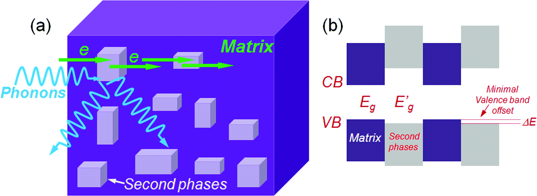 | ||
| Fig. 8 (a) The small valence band offsets allow facile hole transmission through a nanostructured matrix with an endotaxially arranged second phase that simultaneously scatters heat carrying phonons at the matrix/nanostructure interface. (b) Relative energy band diagram for the combined nanostructured matrix showing the large differences in semiconducting band gap and the small energy difference, ΔE, in the valence band edges. | ||
A system where heat flow can be greatly inhibited without affecting the carrier mobility is found in p-type PbTe with endotaxial SrTe nanocrystals. The relative observed insensitivity of hole scattering is attributed to favorable valence band alignment of SrTe and PbTe with 1%Na2Te. As shown in Fig. 9(a), for a control sample of p-type PbTe doped with 1% Na2Te, the carrier mobility at room temperature is ∼350 cm2 V−1 s−1. The corresponding carrier mobility for a sample containing 1% (and 2%) SrTe is ∼340 cm2 V−1 s−1 (for the same carrier concentration of ∼5.6 × 1019 cm−3). The growth of endotaxial SrTe nanocrystals in the PbTe matrix does not appear to affect the hole scattering. This is believed to occur by (1) endotaxial alignment of SrTe and PbTe with coherent/semi-coherent interfaces, and (2) the alignment of the energies of the valence bands in the two materials where the band offset is very small at >300 K. The favorable valence band top alignment of the PbTe and SrTe phases is also suggested by first-principles band calculations. As can be seen from Fig. 9(b) the alignment of the valence band top is favorable and indeed p-type Na doping in the PbTe–SrTe system does result in negligible reduction of the carrier mobility relative to pure PbTe.14
 | ||
| Fig. 9 (a) Temperature dependence of carrier mobilities and lattice thermal conductivity for the PbTe–SrTe system doped with 1% Na2Te. The endotaxial nanostructured SrTe with small valence band offsets allows seamless hole transmission and simultaneously blocks heat carrying phonons at the matrix/nanostructure interface. (b) Schematic representation of the alignment of the valence band (VB) and conduction band (CB) energies of SrTe precipitates in the PbTe matrix. | ||
The PbSe system is another important example where enhancing the thermoelectric performance via matrix/inclusion band alignment can be accomplished. In this case the band energy offsets between the PbSe matrix and the nanostructured phases can be reduced using compositionally alloyed CdS1−xSex/ZnS1−xSe nanostructures.16 As shown in Fig. 10(a), an increase in the second phase fraction results in only small changes in carrier mobilities for the PbSe–(CdS/ZnS). In contrast, a decreasing trend is observed for the CdSe/ZnSe containing samples. It is believed that the variations in carrier mobility are associated with valence band offsets between the host PbSe matrix and the nanostructured second phase precipitates. Density functional theory (DFT) calculations of band alignment show that relative to PbSe, the valence band energy differences are 0.06 eV, 0.27 eV, 0.13 eV and 0.30 eV for CdSe, CdS, ZnSe and ZnS,16 respectively, as shown in Fig. 10(b). The reduced hole mobility for CdSe/ZnSe samples indicates relatively strong scattering of holes across the (CdSe/ZnSe)/PbSe interfaces, whose valence band energy offsets are relatively large. Clearly the band offsets between perfectly ordered, stoichiometric phases are not sufficient to explain the small changes in the carrier mobilities for the PbSe–(CdS/ZnS). However, high resolution energy dispersive spectroscopy (EDS) analysis on these nanoprecipitates suggests that when CdS/ZnS is introduced into the PbSe matrix, they change the composition and become solid solutions of the type CdS1−xSex/ZnS1−xSex. This happens via an interfacial reaction between the sulfide matrix and the selenide second phase. We call these compositionally alloyed nanostructures. When this happens the valence band energy levels for CdS1−xSex/ZnS1−xSex are intermediate between those of CdS/ZnS and CdSe/ZnSe (though not necessarily linear in x; Fig. 10(b) is only a schematic illustration). This effect achieves excellent energy level alignments (minimal offset) with the PbSe matrix. This is also supported by the DFT calculations which suggest that the valence band energy of CdS0.9Se0.1 lies between those of CdS and CdSe.16
 | ||
| Fig. 10 (a) Carrier mobility at room temperature as a function of second phase fractions for Pb0.98Na0.02Se with metal selenides/sulfides, all samples have a similar carrier concentration of ∼3 × 1020 cm−3. The carrier mobilities for the CdS/ZnS containing samples show negligible changes, but show a carrier scattering for CdSe/ZnSe containing samples. This type of band-offset engineering takes advantage of the electronic bands of the non-stoichiometric nanostructures which allow facile carrier transport between matrix and nanostructure. (b) DFT derived conduction band (CB) and valence band (VB) energy levels for PbSe, CdS, CdSe, ZnS and ZnSe. CdS1−xSex and ZnS1−xSex solid solutions show an energy level bridging, all calculations for metal selenides and sulfides are for the NaCl structure. | ||
This is a new type of band-offset engineering that takes advantage of the electronic bands of the compositionally alloyed nanostructures. The second phase nanostructures react with the matrix to become alloyed so that the two band energies in each phase get closer in energy, see eqn (2). Because of the small concentration of the second phase (usually a few mole%) the perturbation of the alloying action on the electronic structure of the matrix is negligible, but it is substantial for that of the second phase.
| PbSe + CdS → PbSe1−xSx + CdS1−xSe | (2) |
This insight can be used to design systems in which the valence and conduction band energies can be aligned between matrix and inclusion. Of course, the embedded nanostructures simultaneously scatter phonons to produce large reductions in lattice thermal conductivity. The combination of these effects amounts to a powerful design strategy for advanced thermoelectrics. It goes beyond the recent ideas of reducing the lattice thermal conductivity through all-scale hierarchical architectures, because it adds to it a new theory-guided concept which is the band alignment engineering across the matrix/inclusion interface. In the case of p-type PbSe an extraordinary ZT of ∼ 1.6 at 923 K is achieved,16 which is the highest value ever reported for a Te-free chalcogenide.
The generality of the matrix/second-phase-inclusion band alignment concept is also evident in its application to the PbS system with metal sulfides, MS (M = Pb, Cd, Zn, Ca and Sr) as the second phases.15,54 The variations of carrier mobility in PbS depend on the valence and conduction band energy levels of the NaCl-type metal sulfides, MS (M = Pb, Cd, Zn, Ca and Sr). The hole/electron transport can be controlled by band offset minimization through the alignment of valence bands between the host PbS and the embedded second phases, MS (M = Cd, Zn, Ca and Sr). This approach gave the highest ZT value of 1.3 at 923 K for p-type Pb0.975Na0.025S–3%CdS.15 The superior ZT of the CdS containing samples comes from a high hole carrier mobility.
The effect of the second phases on both the electron (n-type) and hole (p-type) mobilities in PbS with CdS, ZnS, CaS and SrS is shown in Fig. 11(a). For n-type PbS the electron mobility values at room temperature are significantly reduced. The level of mobility reduction is almost the same regardless of the metal sulfides. This is explained by the relatively strong scattering of electrons in the conduction band of PbS because of the large conduction band offsets (misalignment) between the two phases. This is supported by DFT calculations of the energy barriers which are in the order of >0.5 eV between the conduction bands of PbS and those of the metal sulfides.15,54 Relative to PbS, the respective conduction band energy differences are 0.54 eV, 0.91 eV, 1.09 eV and 1.21 eV for CdS, ZnS, CaS and SrS, respectively, Fig. 11(b). These energy offsets are very large and well exceed the magnitude of thermal energy even at elevated temperatures thereby resulting in strong scattering of conduction electrons.15,54
 | ||
| Fig. 11 (a) Carrier mobility at room temperature for the n-type and p-type PbS with metal sulfides. Small band energy offset for the valence band (VB) between PbS and CdS allows hole transport between the endotaxially aligned components (i.e. matrix and nanostructure), thus minimizing significant deterioration of the hole mobility in p-type PbS. But large band energy offsets for the conduction band (CB) cause decreasing electron mobility due to electron scattering in n-type PbS. (b) DFT band alignments of the conduction band (CB) and valence band (VB) energy levels for PbS, CdS, ZnS, CaS and SrS. All calculations are for metal sulfides in the NaCl structure. | ||
For the p-type PbS system, the situation is very different and far more interesting. The hole mobilities of the CdS containing samples are the highest, Fig. 11(a). Namely, the room temperature carrier mobility is ∼148 cm2 V−1 s−1 for the Pb0.975Na0.025S–3.0% CdS sample, much higher than ∼118 cm2 V−1 s−1, ∼115 cm2 V−1 s−1, and ∼111 cm2 V−1 s−1 for 3.0% ZnS, 3.0% CaS, and 3.0% SrS containing samples (with a similar carrier concentration of 4.78 × 1019 cm−3), respectively. The CdS nanocrystals in the PbS matrix do not appear to significantly affect the hole scattering. The better alignment of energies of the valence band maxima between PbS and CdS (in the NaCl structure) can account for this.
The electronic band structure calculations for PbS and the metal sulfides indicate valence band maxima (VBM) energy differences (with respect to the VBM of PbS) of 0.13 eV, 0.16 eV, 0.53 eV and 0.63 eV for CdS, ZnS, CaS and SrS respectively,15,54 see Fig. 11(b). The minimum band offset is about 0.13 eV with the valence band maximum of PbS lying higher than that of CdS. The energy difference is even greater with the other metal sulfides. Incidentally the band offsets are expected to decrease with rising temperature due to thermal band broadening, thus minimizing significant deterioration of the hole mobility at high temperatures, as shown in Fig. 12.
 | ||
| Fig. 12 Hole mobility at 923 K as a function of energy difference for the valence band maxima between metal sulfides and PbS. The minimizing significant deterioration of the hole mobility at high temperatures indicates that the band energy offset between PbS and CdS decreases with rising temperature due to thermal band broadening. | ||
Besides the lead chalcogenide family, the approach of matrix/inclusion band alignment has been successfully implemented in the SiGe system.72 The electrical conductivity of a Si86.25Ge13.75P1.05 sample was improved by 54% using the modulation-doping approach in (Si95Ge5)0.65(Si70Ge30P3)0.35. The Si nanoparticles form proper band alignments with the SiGe matrix to promote the flow of carriers from the nanoparticles into the matrix. The enhancement in electrical conductivity comes from the 50% improvement of the carrier mobility. Additionally, the thermal conductivity can be kept low due to the low thermal conductivity of the nanoparticles. The enhanced electrical conductivity coupling with negligibly changed Seebeck coefficient and the lower thermal conductivity produces a peak ZT of ∼1.3 at 1173 K in (Si95Ge5)0.65(Si70Ge30P3)0.35.72
Intra-matrix electronic structure engineering
The above mentioned approaches to enhancing the thermoelectric performance involve reducing the lattice thermal conductivity and maintaining the carrier mobility through all-scale hierarchical architectures and band alignment, respectively. There is another performance enhancing mechanism that involves modifying the electronic structure of the matrix itself which can be guided by theory.11–13 In this section, we discuss the addition of intra-matrix band engineering to further increase the power factor and performance. For other mechanisms known to increase Seebeck coefficients see excellent reviews elsewhere.37,38,73Lead chalcogenides, particularly PbTe and PbSe, have a fascinating valence band. In addition to the normal so-called light hole band at the L point of the highly symmetric Brillouin zone there is a second valence (the so-called heavy hole band) band (Σ) which lies energetically below it.11–13,74–77 The p-type carriers can be redistributed into the two different valence bands at high temperatures when they are doped heavily. Because of the cubic symmetry these bands have a very high degeneracy which contributes to the high Seebeck coefficient. The literature going back to the 1960s suggests that as the temperature increases,12,13,77 the L band gradually lowers its energy and passes the Σ band edge at a specific temperature point which is dependent on the energy offsets between L and Σ bands, while the energy for the Σ band remains roughly constant with respect to the conduction band (C band), see Fig. 13(a). In this model, the two valence bands converge rapidly by ∼450 K, and the material changes from a direct-gap to an indirect-gap semiconductor. This view, however, has recently been challenged. New insights deriving from more detailed Hall effect measurements indicate that this convergence is much more slow with rising temperature and likely does not occur until T > 1000 K. The new experimental data suggest that p-type PbTe continues to be a direct-gap semiconductor at temperatures up to 800 K.78 That means no valence band convergence (in energy) happens with increasing temperature. As the temperature increases, the L and Σ band edges may move relative to one another, but does not cross or converge. Instead this movement results in a decrease of the energy offsets between L and Σ bands, Fig. 13(b). Clearly there is a controversy here which will need to be settled with future experimentation.
 | ||
| Fig. 13 Two proposed schematic representations of the relative energies as a function of temperature for two valence bands (L and Σ) in the PbTe system: (a) Relative energy of the valence bands in the PbTe system, at T1 temperature, the two valence bands converge, resulting in transport contributions from both the L and Σ bands. (b) New view of the relative energy of the valence bands in the PbTe system, no two valence bands converge up to T2 temperature, the transport contributions result from the carriers injecting from the Σ band to the L band. | ||
In this new view, as the energy offsets between L and Σ bands decrease the heavy valence band contributes to the transport via thermal excitation of holes from L to Σ. Generally, the contribution of the heavy valence band to the Seebeck coefficient can be realized via heavy doping because this lowers the Fermi energy and decreases the energy offsets between L and Σ bands. Thus, the contribution of the heavy valence band is observed at a lower temperature through heavy doping.11–13 As shown in Fig. 14(a), p-type PbTe shows higher Seebeck coefficients than that of n-type PbTe with a similar carrier concentration of ∼3 × 1019 cm−3, especially at elevated temperatures. Namely, the Seebeck coefficient at 773 K is ∼ +270 μV K−1 for p-type PbTe, whereas by comparison it is only ∼−180 μV K−1 for similarly doped n-type PbTe.16,37,73,79 The excess Seebeck coefficient is attributed to the contribution of the Σ band. The n-type samples do not exhibit such contribution because of the single band nature of the conduction band. The generation of holes in the Σ band further enhances the Seebeck coefficient because of the high effective mass m* of these holes. The enhancement is by a factor of Nv2/3, where Nv is the number of degenerate valleys, Nv is 4 for the L band and increases to 12 for the Σ band. Specifically, m* = Nv2/3m*b, where m*b is the average (single valley) effective mass of the degenerate valleys.16,32,37,73
 | ||
| Fig. 14 (a) Seebeck coefficients as a function of temperature for lead chalcogenides PbQ (Q = Te, Se and S), Seebeck coefficients are enhanced in p-type materials compared with n-type analogues with a similar carrier concentration due to the heavy valence band convergence for PbTe and PbSe systems, similar Seebeck coefficients indicate that no heavy valence band is involved in the PbS system at the temperature up to 923 K. (b) Carrier concentration as a function of temperature for PbQ (Q = Te, Se and S), the upturns of carrier concentrations in PbTe and PbSe systems indicate the contribution of the heavy valence band. | ||
Similarly, p-type and n-type PbSe exhibit the same magnitude of Seebeck coefficients at room temperature, the carrier concentration for both types is fixed at a similar value of ∼3 × 1020 cm−3.16 However, the magnitude of the Seebeck coefficient for the p-type PbSe sample starts to deviate from n-type PbSe, and becomes much larger with rising temperature. At 923 K, the Seebeck coefficient reaches ∼+250 μV K−1 for p-type PbSe, whereas by comparison it is only ∼−100 μV K−1 for similarly doped n-type PbSe.16 The doubling of the Seebeck coefficients in p-type PbTe and PbSe samples is related to the involvement of the Σ band at high temperatures.
In the PbS system both p-type and n-type materials exhibit similar Seebeck coefficients up to 923 K indicating no heavy valence band involvement. This different behavior from PbTe and PbSe results from the much larger L–Σ energy separation, which is about 0.40 eV.80 Notably, for the same carrier concentration, it can be seen that p-type PbS shows a slightly higher Seebeck coefficient of ∼+200 μV K−1 than that of ∼−185 μV K−1 for n-type PbS at ∼923 K.34,54 This may be a sign of the onset of the heavy valence band contribution. The carrier concentrations in Fig. 14(b) show an apparent rise with the temperature in p-type PbTe and p-type PbSe but not in n-type PbSe or p-type PbS. This thermal increase in carriers is artificial and originates from the incorrect assumption of single band transport. In p-type PbTe, the contribution of the heavy valence band is apparent at ∼400 K, compared to ∼673 K for p-type PbSe. For p-type PbS, because of the larger energy difference between L and Σ bands, the contribution is barely observed at ∼923 K.
As mentioned above, the thermal excitation of holes from the L to the Σ band with rising temperature creates carriers in the Σ band with dramatically higher effective mass. Compositional alloying in the matrix may result in a change of the energies of L and Σ bands. Examples are Mn, Mg and Cd alloying in PbTe where the energy difference between L and Σ bands was reported to decrease with respect to the alloying fractions.81–86 DFT calculations indicate that compositional alloying of the type Pb1−xMxQ (Q = Te and Se) may have significant effect on the energies of both L and Σ bands,12,74,81–84,87Fig. 15(a). With increasing solid solution fraction of M, both L and Σ bands lower their energies, but the L band moves faster than the Σ band, so that the two bands move closer, Fig. 15(b). At the same time, if the second phase has a larger band gap than the matrix, increasing concentrations of it can increase the band gap of the matrix, i.e. the energy between L and conduction C bands (ΔEC–L), Fig. 15(c). Generally, in these systems the calculations show that the energy of the Σ band remains roughly constant with respect to the C band. Therefore, this type of solid solution alloying enables the enhancement of the Seebeck coefficient. A typical example is Cd alloying in PbSe.16,82,84 The alloying of Cd on the cation sublattice of PbSe makes Pb1−xCdxSe more similar to PbTe in terms of the heavy valence band convergence. The Seebeck coefficient enhancement is similar in character to that caused by resonant states.38 Namely, the Cd containing samples show enhancements of 10 μV K−1 and 25 μV K−1 in the Seebeck coefficient at 300 K and 923 K, respectively. This enhancement is attributed to the intra-matrix electronic structure engineering described above and it is key to achieving the high ZT of 1.6 at 923 K.16
 | ||
| Fig. 15 (a) Schematic showing the relative energy of the valence bands in PbQ (Q = Te and Se) systems, with rising solid solution fraction (such as Mn, Mg and Cd etc.). The solid solution alloying within the solubility limit modifies the valence band structure push both L and Σ bands move down but make the two valence bands closer in energy. (b) Plot of the relative band energy for the conduction band (C), light valence (L) band and heavy valence (Σ) band as a function of the solid solution phase fractions in PbQ (Q = Te and Se) systems. (c) Plot of the band energy differences as a function of the solid solution phase fractions in PbQ (Q = Te and Se) systems. | ||
The intra-matrix band engineering described above has also been successfully applied to other systems such as the Mg2Si–Mg2Sn27 and the SnTe.88 At a given composition of x, Mg2Si1−xSnx solid solutions display a convergence in energy of the two conduction bands. Transport measurements carried out from 4 K to 800 K reveal a progressively increasing Seebeck coefficient that peaks at x = 0.7. At this concentration the ZT reaches a high value of 1.3 near 700 K.27 The high Seebeck coefficient and ZT values seem to originate from an enhanced effective mass brought about by the increased valley degeneracy as the two conduction bands converge in energy. In the SnTe system, (Ag0.366Sb0.558Te)1−x(SnTe)x solid solutions covering the entire pseudo-binary phase diagram were reported to show complete solubility.88 The transport properties show that there must be a valence convergence at x ∼ 0.2–0.27, possibly due to Ag0.366Sb0.558Te-like valence band difference and SnTe-like Σ band crossing, thus in an enhancement of Seebeck coefficients. At T > 500 K, two compositions show a maximum ZT of ∼0.9 at x∼20–25% near the composition of (Ag0.366Sb0.558Te)1−x(SnTe)x solid solutions.88 This explanation may be relevant to the related system AgSnmSbTe2+m which also shows enhanced properties relative to SnTe itself.89
Synergy of mechanisms leads to high thermoelectric performance
If all the above mechanisms and approaches could be independently controlled and integrated into a single material system we can expect a very high performance via what could be called a synergistic effect. This has been demonstrated in the PbTe system. Some time ago, Kudman et al.90 first reported the Na doped PbTe–PbSe system to have an enhanced power factor compared to PbTe resulting in a high ZT of 1.35 at 650 K for 0.7% Na doped PbTe with 15% Se alloying. Pei et al.32 later reinvestigated the system utilizing higher doping levels and achieved a ZT of 1.8 at 850 K for 2% Na doped PbTe with 15% Se alloying. Pei et al. attributed the high ZT to the convergence of multiple degenerate valley pockets at the Fermi level to effectively increase the effective mass without negatively impacting the mobility; the Se alloy tunes the location of the valence band to achieve this increased degeneracy at the Fermi level leading to very high power factors and high ZT. The lattice thermal conductivity of the system is well described by an alloy scattering model.91 Even though no TEM afforded, the low lattice thermal conductivity obtained for 2% Na doped PbTe0.85Se0.15 may be partially due to nanostructures.Another example of high performance which involves nanostructuring and heavy valence band engineering is realized in the Na doped PbTe–PbS system.48 In this case both nanostructure formation and modification of the electronic structure can be controlled to significantly enhance the power factor. These synergistic effects result in a maximum ZT of ∼1.8 at 800 K;48 by applying mesostructuring to this system a ZT of ∼2.0 may be obtained.
A more interesting example is the PbSe–CdS system,16 see Fig. 16. A design strategy here which provides an effective approach integrating different but synergistic concepts is as follows: (a) intra-matrix band structure convergence, (b) inter-phase PbSe/CdS band alignment, and band energy offset minimization; and (c) with all-scale hierarchical nano-/meso-structuring, one can push ZT of heavily doped p-type PbSe to reach ∼1.6 at 923 K.
 | ||
| Fig. 16 Cumulative integration of material approaches as a function of the thermoelectric figure of merit, ZT, for the PbSe system, indicating that ZT can be increased through a combination of synergistic approaches including all-scale hierarchical architectures, intra-matrix band engineering and matrix/inclusion band engineering. | ||
Summary and outlook
In the past decade a number of new concepts have emerged which can be integrated in a synergistic manner in bulk materials to greatly enhance their ZT to levels that could only be dreamed of a decades ago. Clearly, we have entered a new era for thermoelectric materials research. Historically, the increase in ZT came from the reduction of lattice thermal conductivity. In this review, we have highlighted that ZT can be raised successively by continuously integrating performance enhancing concepts into a single material system. Fig. 16 shows the best illustration of this by showing how these different concepts can work together (synergy) to raise ZT. To date, the scattering of phonons by all-scale hierarchical architectures in bulk materials is an established paradigm which in the case of PbTe can achieve a lattice thermal conductivity of ∼0.5 W m−1 K−1. Further improvements may get us closer to the “minimal lattice thermal conductivity” value of 0.36 W m−1 K−1 as calculated for Pb–Te–Se by the approach of Cahill.92 Chen et al.6 have even suggested that the minimum thermal conductivity in nanostructures is likely lower than that in bulk materials. This is because the minimum thermal conductivity theory for bulk materials is based on isotropic scattering, while in nanostructures, interfacial scattering is highly anisotropic. Therefore, there seems to be further room for higher ZT values, possibly in the ∼2.5–3.0 range in PbTe and ∼2.0 in PbSe provided we can achieve this minimum thermal conductivity in nanostructures. The panoscopic approach has the potential to enhance the performance of systems with intrinsically high thermal conductivity, for example, Mg2Si,27,93 Half-Heusler compounds,25,26,46 and Skutterudites23,24,94–99etc.Future research that aims to enhance the power factor is important and timely and will define upcoming efforts in this field. The much anticipated use of resonance states to increase the Seebeck coefficient and the overall power factor29,38 has not yet been realized above room temperature. In addition, the heavy valence band involved in enhancing the Seebeck coefficient in p-type lead chalcogenides may analogously be extended to conduction band engineering for suitable n-type systems. Simultaneously, band structure engineering provides guiding principles in the optimization of existing thermoelectric materials. These power factor enhancing approaches would be very promising for applying them in compounds with intrinsically low thermal conductivity.100–111
Besides focusing on enhancing the thermoelectric performance, extensive work has been carried out to assess and understand the mechanical properties112–119 which also are critical in the thermoelectric community when considering device fabrication. Although these were not the focus of this article they are of great importance as a subject of investigation. Understanding issues of mechanical robustness in the new high performance materials will help open the path to device assembly, testing and ultimately commercialization.120
Acknowledgements
This work was supported in part by a grant DOE-EERE/NSF (CBET-1048728), the Revolutionary Materials for Solid State Energy Conversion, an Energy Frontier Research Center funded by the U.S. Department of Energy, Office of Science, and Office of Basic Energy Sciences under Award Number DE-SC0001054. We also acknowledge the use of the transmission electron microscope from NUANCE Center at Northwestern University. We thank Professors C. Uher, C. Wolverton, D. N. Seidman, T. P. Hogan, J. P. Heremans, and E. D. Case for plentiful discussions and fruitful collaborations.References
- M. G. Kanatzidis, Chem. Mater., 2010, 22, 648–659 CrossRef CAS.
- J. R. Sootsman, D. Y. Chung and M. G. Kanatzidis, Angew. Chem., Int. Ed., 2009, 48, 8616–8639 CrossRef CAS PubMed.
- C. J. Vineis, A. Shakouri, A. Majumdar and M. G. Kanatzidis, Adv. Mater., 2010, 22, 3970–3980 CrossRef CAS PubMed.
- A. Shakouri, Annu. Rev. Mater. Res., 2011, 41, 399–431 CrossRef CAS.
- G. J. Snyder and E. S. Toberer, Nat. Mater., 2008, 7, 105–114 CrossRef CAS PubMed.
- A. J. Minnich, M. S. Dresselhaus, Z. F. Ren and G. Chen, Energy Environ. Sci., 2009, 2, 466–479 CAS.
- J. F. Li, W. S. Liu, L. D. Zhao and M. Zhou, NPG Asia Mater., 2010, 2, 152–158 CrossRef.
- J. P. Heremans, M. S. Dresselhaus, L. E. Bell and D. T. Morelli, Nat. Nanotechnol., 2013, 8, 471–473 CrossRef CAS PubMed.
- W. S. Liu, X. Yan, G. Chen and Z. Ren, Nano Energy, 2012, 1, 42–56 CrossRef CAS PubMed.
- P. Pichanusakorn and P. Bandaru, Mater. Sci. Eng., R, 2010, 67, 19–63 CrossRef PubMed.
- H. Heinrich, K. Lischka, H. Sitter and M. Kriechbaum, Phys. Rev. Lett., 1975, 35, 1107–1110 CrossRef CAS.
- H. Sitter, K. Lischka and H. Heinrich, Phys. Rev. B: Solid State, 1977, 16, 680–687 CrossRef CAS.
- N. V. Kolomotes, M. N. Vinogradova and L. M. Sysoeva, Semiconductors, 1968, 1, 1020–1023 Search PubMed.
- K. Biswas, J. Q. He, Q. C. Zhang, G. Y. Wang, C. Uher, V. P. Dravid and M. G. Kanatzidis, Nat. Chem., 2011, 3, 160–166 CrossRef CAS PubMed.
- L. D. Zhao, J. Q. He, S. Q. Hao, C. I. Wu, T. P. Hogan, C. Wolverton, V. P. Dravid and M. G. Kanatzidis, J. Am. Chem. Soc., 2012, 134, 16327–16336 CrossRef CAS PubMed.
- L. D. Zhao, S. Hao, S. H. Lo, C. I. Wu, X. Zhou, Y. Lee, H. Li, K. Biswas, T. P. Hogan, C. Uher, C. Wolverton, V. P. Dravid and M. G. Kanatzidis, J. Am. Chem. Soc., 2013, 135, 7364–7370 CrossRef CAS PubMed.
- K. Biswas, J. Q. He, I. D. Blum, C. I. Wu, T. P. Hogan, D. N. Seidman, V. P. Dravid and M. G. Kanatzidis, Nature, 2012, 489, 414–418 CrossRef CAS PubMed.
- D. Y. Chung, T. Hogan, P. Brazis, M. Rocci-Lane, C. Kannewurf, M. Bastea, C. Uher and M. G. Kanatzidis, Science, 2000, 287, 1024–1027 CrossRef CAS.
- B. Poudel, Q. Hao, Y. Ma, Y. Lan, A. Minnich, B. Yu, X. Yan, D. Wang, A. Muto, D. Vashaee, X. Chen, J. Liu, M. S. Dresselhaus, G. Chen and Z. Ren, Science, 2008, 320, 634–638 CrossRef CAS PubMed.
- W.-S. Liu, Q. Zhang, Y. Lan, S. Chen, X. Yan, Q. Zhang, H. Wang, D. Wang, G. Chen and Z. Ren, Adv. Energy Mater., 2011, 1, 577–587 CrossRef CAS.
- (a) K. F. Hsu, S. Loo, F. Guo, W. Chen, J. S. Dyck, C. Uher, T. Hogan, E. K. Polychroniadis and M. G. Kanatzidis, Science, 2004, 303, 818–821 CrossRef CAS PubMed; (b) D. Bilc, S. D. Mahanti, E. Quarez, K. F. Hsu, R. Pcionek and M. G. Kanatzidis, Phys. Rev. Lett., 2004, 93, 146403 CrossRef; (c) E. Quarez, K. F. Hsu, R. Pcionek, N. Frangis, E. K. Polychroniadis and M. G. Kanatzidis, J. Am. Chem. Soc., 2005, 127, 9177–9190 CrossRef CAS PubMed; (d) B. A. Cook, M. J. Kramer, J. L. Harringa, M. K. Han, D. Y. Chung and M. G. Kanatzidis, Adv. Funct. Mater., 2009, 19, 1254–1259 CrossRef CAS.
- A. Saramat, G. Svensson, A. E. C. Palmqvist, C. Stiewe, E. Mueller, D. Platzek, S. G. K. Williams, D. M. Rowe, J. D. Bryan and G. D. Stucky, J. Appl. Phys., 2006, 99, 023708 CrossRef.
- X. Shi, J. Yang, J. R. Salvador, M. Chi, J. Y. Cho, H. Wang, S. Bai, J. Yang, W. Zhang and L. Chen, J. Am. Chem. Soc., 2011, 133, 7837–7846 CrossRef CAS PubMed.
- G. Rogl, D. Setman, E. Schafler, J. Horky, M. Kerber, M. Zehetbauer, M. Falmbigl, P. Rogl, E. Royanian and E. Bauer, Acta Mater., 2012, 60, 2146–2157 CrossRef CAS PubMed.
- G. Joshi, T. Dahal, S. Chen, H. Z. Wang, J. Shiomi, G. Chen and Z. F. Ren, Nano Energy, 2013, 2, 82–87 CrossRef CAS PubMed.
- X. Yan, W. S. Liu, H. Wang, S. Chen, J. Shiomi, K. Esfarjani, H. Z. Wang, D. Z. Wang, G. Chen and Z. F. Ren, Energy Environ. Sci., 2012, 5, 7543–7548 CAS.
- W. Liu, X. Tan, K. Yin, H. Liu, X. Tang, J. Shi, Q. Zhang and C. Uher, Phys. Rev. Lett., 2012, 108, 166601 CrossRef.
- J. Androulakis, C. H. Lin, H. J. Kong, C. Uher, C. I. Wu, T. Hogan, B. A. Cook, T. Caillat, K. M. Paraskevopoulos and M. G. Kanatzidis, J. Am. Chem. Soc., 2007, 129, 9780–9788 CrossRef CAS PubMed.
- J. P. Heremans, V. Jovovic, E. S. Toberer, A. Saramat, K. Kurosaki, A. Charoenphakdee, S. Yamanaka and G. J. Snyder, Science, 2008, 321, 554–557 CrossRef CAS PubMed.
- J. S. Rhyee, K. H. Lee, S. M. Lee, E. Cho, S. I. Kim, E. Lee, Y. S. Kwon, J. H. Shim and G. Kotliar, Nature, 2009, 459, 965–968 CrossRef CAS PubMed.
- S. N. Girard, J. He, X. Zhou, D. Shoemaker, C. M. Jaworski, C. Uher, V. P. Dravid, J. P. Heremans and M. G. Kanatzidis, J. Am. Chem. Soc., 2011, 133, 16588–16597 CrossRef CAS PubMed.
- Y. Pei, X. Shi, A. LaLonde, H. Wang, L. Chen and G. J. Snyder, Nature, 2011, 473, 66–69 CrossRef CAS PubMed.
- J. Androulakis, I. Todorov, J. He, D. Y. Chung, V. Dravid and M. Kanatzidis, J. Am. Chem. Soc., 2011, 133, 10920–10927 CrossRef CAS PubMed.
- L. D. Zhao, S. H. Lo, J. He, H. Li, K. Biswas, J. Androulakis, C. I. Wu, T. P. Hogan, D. Y. Chung, V. P. Dravid and M. G. Kanatzidis, J. Am. Chem. Soc., 2011, 133, 20476–20487 CrossRef CAS PubMed.
- X. W. Wang, H. Lee, Y. C. Lan, G. H. Zhu, G. Joshi, D. Z. Wang, J. Yang, A. J. Muto, M. Y. Tang, J. Klatsky, S. Song, M. S. Dresselhaus, G. Chen and Z. F. Ren, Appl. Phys. Lett., 2008, 93, 193121 CrossRef.
- J. He, M. G. Kanatzidis and V. P. Dravid, Mater. Today, 2013, 16, 166–176 CrossRef CAS PubMed.
- Y. Pei, H. Wang and G. J. Snyder, Adv. Mater., 2012, 24, 6125–6135 CrossRef CAS PubMed.
- J. P. Heremans, B. Wiendlocha and A. M. Chamoire, Energy Environ. Sci., 2012, 5, 5510–5530 CAS.
- H. Kleinke, Chem. Mater., 2010, 22, 604–611 CrossRef CAS.
- E. S. Toberer, A. F. May and G. J. Snyder, Chem. Mater., 2010, 22, 624–634 CrossRef CAS.
- K. Koumoto, R. Funahashi, E. Guilmeau, Y. Miyazaki, A. Weidenkaff, Y. Wang, C. Wan and X. D. Zhou, J. Am. Ceram. Soc., 2013, 96, 1–23 CrossRef CAS.
- J. Yang, H. L. Yip and A. K. Y. Jen, Adv. Energy Mater., 2013, 3, 549–565 CrossRef CAS.
- C. Wan, Y. Wang, N. Wang, W. Norimatsu, M. Kusunoki and K. Koumoto, Sci. Technol. Adv. Mater., 2010, 11, 044306 CrossRef.
- D. L. Medlin and G. J. Snyder, Curr. Opin. Colloid Interface Sci., 2009, 14, 226–235 CrossRef CAS PubMed.
- P. Vaqueiro and A. V. Powell, J. Mater. Chem., 2010, 20, 9577 RSC.
- L. D. Chen, X. Y. Huang, M. Zhou, X. Shi and W. B. Zhang, J. Appl. Phys., 2006, 99, 064305 CrossRef.
- W. Kim, J. Zide, A. Gossard, D. Klenov, S. Stemmer, A. Shakouri and A. Majumdar, Phys. Rev. Lett., 2006, 96, 045901 CrossRef.
- S. N. Girard, J. Q. He, C. P. Li, S. Moses, G. Y. Wang, C. Uher, V. P. Dravid and M. G. Kanatzidis, Nano Lett., 2010, 10, 2825–2831 CrossRef CAS PubMed.
- J. Androulakis, K. F. Hsu, R. Pcionek, H. Kong, C. Uher, J. J. Dangelo, A. Downey, T. Hogan and M. G. Kanatzidis, Adv. Mater., 2006, 18, 1170–1173 CrossRef CAS.
- P. F. R. Poudeu, J. D'Angelo, A. D. Downey, J. L. Short, T. P. Hogan and M. G. Kanatzidis, Angew. Chem., Int. Ed., 2006, 45, 3835–3839 CrossRef CAS PubMed.
- K. Ahn, M. K. Han, J. Q. He, J. Androulakis, S. Ballikaya, C. Uher, V. P. Dravid and M. G. Kanatzidis, J. Am. Chem. Soc., 2010, 132, 5227–5235 CrossRef CAS PubMed.
- K. Biswas, J. Q. He, G. Y. Wang, S. H. Lo, C. Uher, V. P. Dravid and M. G. Kanatzidis, Energy Environ. Sci., 2011, 4, 4675–4684 CAS.
- Y. Lee, S. H. Lo, J. Androulakis, C. I. Wu, L. D. Zhao, D. Y. Chung, T. P. Hogan, V. P. Dravid and M. G. Kanatzidis, J. Am. Chem. Soc., 2013, 135, 5152–5160 CrossRef CAS PubMed.
- L. D. Zhao, J. Q. He, C. I. Wu, T. P. Hogan, X. Y. Zhou, C. Uher, V. P. Dravid and M. G. Kanatzidis, J. Am. Chem. Soc., 2012, 134, 7902–7912 CrossRef CAS PubMed.
- J. R. Sootsman, R. J. Pcionek, H. J. Kong, C. Uher and M. G. Kanatzidis, Chem. Mater., 2006, 18, 4993–4995 CrossRef CAS.
- J. Q. He, J. Androulakis, M. G. Kanatzidis and V. P. Dravid, Nano Lett., 2012, 12, 343–347 CrossRef CAS PubMed.
- Y. Lan, A. J. Minnich, G. Chen and Z. Ren, Adv. Funct.Mater., 2010, 20, 357–376 CrossRef CAS.
- D. M. Rowe and V. S. Shukla, J. Appl. Phys., 1981, 52, 7421–7426 CrossRef CAS.
- J. E. Parrott, J. Phys. C: Solid State Phys., 1969, 2, 147–151 Search PubMed.
- N. Savvides and H. J. Goldsmid, Phys. Lett. A, 1972, 41, 193–194 CrossRef CAS.
- A. S. Henry and G. Chen, J. Comput. Theor. Nanosci., 2008, 5, 141–152 CAS.
- Z. Tian, K. Esfarjani, J. Shiomi, A. S. Henry and G. Chen, Appl. Phys. Lett., 2011, 99, 053122 CrossRef.
- B. Qiu, H. Bao, G. Q. Zhang, Y. Wu and X. L. Ruan, Comput. Mater. Sci., 2012, 53, 278–285 CrossRef CAS PubMed.
- Y. Z. Pei, A. LaLonde, S. Iwanaga and G. J. Snyder, Energy Environ. Sci., 2011, 4, 2085–2089 CAS.
- A. D. LaLonde, Y. Z. Pei and G. J. Snyder, Energy Environ. Sci., 2011, 4, 2090–2096 CAS.
- Y. Pei, J. Lensch-Falk, E. S. Toberer, D. L. Medlin and G. J. Snyder, Adv. Funct. Mater., 2011, 21, 241–249 CrossRef CAS.
- J. Androulakis, D. Y. Chung, X. L. Su, L. Zhang, C. Uher, T. C. Hasapis, E. Hatzikraniotis, K. M. Paraskevopoulos and M. G. Kanatzidis, Phys. Rev. B: Condens. Matter Mater. Phys., 2011, 84, 155207 CrossRef.
- H. W. Peng, J. H. Song, M. G. Kanatzidis and A. J. Freeman, Phys. Rev. B: Condens. Matter Mater. Phys., 2011, 84, 125207 CrossRef.
- H. Wang, Y. Z. Pei, A. D. LaLonde and G. J. Snyder, Proc. Natl. Acad. Sci. U. S. A., 2012, 109, 9705–9709 CrossRef CAS PubMed.
- H. Wang, Y. Z. Pei, A. D. LaLonde and G. J. Snyder, Adv. Mater., 2011, 23, 1366–1370 CrossRef CAS PubMed.
- R. Venkatasubramanian, E. Siivola, T. Colpitts and B. O'Quinn, Nature, 2001, 413, 597–602 CrossRef CAS PubMed.
- B. Yu, M. Zebarjadi, H. Wang, K. Lukas, H. Z. Wang, D. Z. Wang, C. Opeil, M. Dresselhaus, G. Chen and Z. F. Ren, Nano Lett., 2012, 12, 2077–2082 CrossRef CAS PubMed.
- A. D. LaLonde, Y. Z. Pei, H. Wang and G. J. Snyder, Mater. Today, 2011, 14, 526–532 CrossRef CAS.
- M. N. Vinogradova, V. I. Tamarchenko and L. V. Prokofeva, Semiconductors, 1975, 9, 318–320 Search PubMed.
- A. J. Crocker and L. M. Rogers, Br. J. Appl. Phys., 1967, 18, 563–573 CrossRef CAS.
- F. U. Galeeva, K. D. Tarzimanov and I. K. Akhmetshin, Inorg. Mater., 1988, 24, 418–420 Search PubMed.
- T. Grandke, M. Cardona and L. Ley, Solid State Commun., 1979, 32, 353–356 CrossRef CAS.
- C. M. Jaworski, M. D. Nielsen, H. Wang, S. N. Girard, W. Cai, W. D. Porter, M. G. Kanatzidis and J. P. Heremans, Phys. Rev. B: Condens. Matter Mater. Phys., 2013, 87, 045203 CrossRef.
- Y. Z. Pei, N. A. Heinz, A. LaLonde and G. J. Snyder, Energy Environ. Sci., 2011, 4, 3640–3645 CAS.
- Y. I. Ravich, B. A. Efimova and I. A. Smirnov, Semiconducting Lead Chalcogenides, Plenum, New York, 1970, vol. 5 Search PubMed.
- A. J. Crocker and B. J. Sealy, J. Phys. Chem. Solids, 1972, 33, 2183–2190 CrossRef CAS.
- B. J. Sealy and A. J. Crocker, J. Mater. Sci., 1973, 8, 1247–1252 CrossRef CAS.
- L. M. Rogers and A. J. Crocker, J. Phys. D: Appl. Phys., 1971, 4, 1016–1024 CAS.
- L. M. Rogers and A. J. Crocker, J. Phys. D: Appl. Phys., 1972, 5, 1671–1679 CAS.
- (a) Y. Z. Pei, A. D. LaLonde, N. A. Heinz, X. Y. Shi, S. Iwanaga, H. Wang, L. D. Chen and G. J. Snyder, Adv. Mater., 2011, 23, 5674–5678 CrossRef CAS PubMed; (b) L. D. Zhao, H. J. Wu, S. Q. Hao, C. I. Wu, X. Y. Zhou, K. Biswas, J. Q. He, T. P. Hogan, C. Uher, C. Wolverton, V. P. Dravid and M. G. Kanatzidis, Energy Environ. Sci., 2013, 6, 3346–3355 RSC.
- Y. Z. Pei, H. Wang, Z. M. Gibbs, A. D. LaLonde and G. J. Snyder, NPG Asia Mater., 2012, 4, e28 CrossRef.
- L. M. Rogers and A. J. Crocker, J. Phys. D: Appl. Phys., 1971, 4, 1006–1015 CAS.
- Y. Chen, M. D. Nielsen, Y.-B. Gao, T. J. Zhu, X. Zhao and J. P. Heremans, Adv. Energy Mater., 2012, 2, 58–62 CrossRef CAS.
- M.-K. Han, J. Androulakis, S.-J. Kim and M. G. Kanatzidis, Adv. Energy Mater., 2012, 2, 157–161 CrossRef CAS.
- I. Kudman, J. Mater. Sci., 1972, 7, 1027–1029 CrossRef CAS.
- T. Murakami, T. Shiga, T. Hori, K. Esfarjani and J. Shiomi, EPL, 2013, 102, 46002 CrossRef.
- Y. K. Koh, C. J. Vineis, S. D. Calawa, M. P. Walsh and D. G. Cahill, Appl. Phys. Lett., 2009, 94, 153101 CrossRef.
- Q. Zhang, J. He, T. J. Zhu, S. N. Zhang, X. B. Zhao and T. M. Tritt, Appl. Phys. Lett., 2008, 93, 102109 CrossRef.
- W. S. Liu, B. P. Zhang, L. D. Zhao and J. F. Li, Chem. Mater., 2008, 20, 7526–7531 CrossRef CAS.
- Z. Xiong, X. Chen, X. Huang, S. Bai and L. Chen, Acta Mater., 2010, 58, 3995–4002 CrossRef CAS PubMed.
- X. Y. Zhao, X. Shi, L. D. Chen, W. Q. Zhang, S. Q. Bai, Y. Z. Pei, X. Y. Li and T. Goto, Appl. Phys. Lett., 2006, 89, 092121 CrossRef.
- G. Tan, S. Wang, H. Li, Y. Yan and X. Tang, J. Solid State Chem., 2012, 187, 316–322 CrossRef CAS PubMed.
- G. Tan, S. Wang, X. Tang, H. Li and C. Uher, J. Solid State Chem., 2012, 196, 203–208 CrossRef CAS PubMed.
- Y. G. Yan, W. Wong-Ng, J. A. Kaduk, G. J. Tan, W. J. Xie and X. F. Tang, Appl. Phys. Lett., 2011, 98, 142106 CrossRef.
- F. Li, J. F. Li, L. D. Zhao, K. Xiang, Y. Liu, B. P. Zhang, Y. H. Lin, C. W. Nan and H. M. Zhu, Energy Environ. Sci., 2012, 5, 7188–7195 CAS.
- J. Li, J. H. Sui, Y. L. Pei, C. Barreteau, D. Berardan, N. Dragoe, W. Cai, J. Q. He and L. D. Zhao, Energy Environ. Sci., 2012, 5, 8543–8547 CAS.
- Y. Liu, L. D. Zhao, Y. C. Liu, J. L. Lan, W. Xu, F. Li, B. P. Zhang, D. Berardan, N. Dragoe, Y. H. Lin, C. W. Nan, J. F. Li and H. M. Zhu, J. Am. Chem. Soc., 2011, 133, 20112–20115 CrossRef CAS PubMed.
- L. D. Zhao, D. Berardan, Y. L. Pei, C. Byl, L. Pinsard-Gaudart and N. Dragoe, Appl. Phys. Lett., 2010, 97, 092118 CrossRef.
- D. T. Morelli, V. Jovovic and J. P. Heremans, Phys. Rev. Lett., 2008, 101, 035901 CrossRef CAS.
- L. Pan, D. Berardan and N. Dragoe, J. Am. Chem. Soc., 2013, 135, 4914–4917 CrossRef CAS PubMed.
- M. D. Nielsen, V. Ozolins and J. P. Heremans, Energy Environ. Sci., 2013, 6, 570–578 CAS.
- Y. L. Pei, H. Wu, J. Sui, J. Li, D. Berardan, C. Barreteau, L. Pan, N. Dragoe, W. S. Liu, J. He and L. D. Zhao, Energy Environ. Sci., 2013, 6, 1750–1755 CAS.
- K. Biswas, L. D. Zhao and M. G. Kanatzidis, Adv. Energy Mater., 2012, 2, 634–638 CrossRef CAS.
- J. Sui, J. Li, J. He, Y. Pei, D. Berardan, N. Dragoe, H. Wu, W. Cai and L. D. Zhao, Energy Environ. Sci., 2013, 6, 2916–2920 CAS.
- Y. Pei, J. He, J.-F. Li, F. Li, Q. Liu, W. Pan, C. Barreteau, D. Berardan, N. Dragoe and L. D. Zhao, NPG Asia Mater., 2013, 5, e47 CrossRef CAS.
- Y. Liu, J. Lan, W. Xu, Y. Liu, Y. Pei, B. Cheng, D. B. Liu, Y.-H. Lin and L. D. Zhao, Chem. Commun., 2013, 49, 8075–8077 RSC.
- L. D. Zhao, B.-P. Zhang, J.-F. Li, M. Zhou, W. S. Liu and J. Liu, J. Alloys Compd., 2008, 455, 259–264 CrossRef CAS PubMed.
- J. D'Angelo, E. D. Case, N. Matchanov, C. I. Wu, T. P. Hogan, J. Barnard, C. Cauchy, T. Hendricks and M. G. Kanatzidis, J. Electron. Mater., 2011, 40, 2051–2062 CrossRef CAS PubMed.
- X. Fan, E. D. Case and M. J. Baumann, J. Mater. Sci., 2012, 47, 6333–6345 CrossRef CAS PubMed.
- A. Q. Morrison, E. D. Case, F. Ren, A. J. Baumann, D. C. Kleinow, J. E. Ni, T. P. Hogan, J. D'Angelo, N. A. Matchanov, T. J. Hendricks, N. K. Karri, C. Cauchy, J. Barnard and M. G. Kanatzidis, Mater. Chem. Phys., 2012, 134, 973–987 CrossRef CAS PubMed.
- J. E. Ni, E. D. Case, J. S. Sakamoto, E. Rangasamy and J. B. Wolfenstine, J. Mater. Sci., 2012, 47, 7978–7985 CrossRef CAS.
- J. E. Ni, E. D. Case, R. Stewart, C. I. Wu, T. P. Hogan and M. G. Kanatzidis, J. Electron. Mater., 2012, 41, 1153–1158 CrossRef CAS PubMed.
- R. D. Schmidt, E. D. Case, J. Giles, J. E. Ni and T. P. Hogan, J. Electron. Mater., 2012, 41, 1210–1216 CrossRef CAS.
- R. D. Schmidt, E. D. Case, G. J. Lehr and D. T. Morelli, Intermetallics, 2013, 35, 15–24 CrossRef CAS PubMed.
- D. Kraemer, B. Poudel, H. P. Feng, J. C. Caylor, B. Yu, X. Yan, Y. Ma, X. W. Wang, D. Z. Wang, A. Muto, K. McEnaney, M. Chiesa, Z. F. Ren and G. Chen, Nat. Mater., 2011, 10, 532–538 CrossRef CAS PubMed.
| This journal is © The Royal Society of Chemistry 2014 |