 Open Access Article
 This Open Access Article is licensed under a
 Creative Commons Attribution 3.0 Unported Licence
Nanoporous dual-electrodes with millimetre extensions: parallelized fabrication and area effects on redox cycling†
Martin
Hüske
a,
Andreas
Offenhäusser
ab and
Bernhard
Wolfrum
*ab
aInstitute of Bioelectronics (PGI-8/ICS-8) and JARA—Fundamentals of Future Information Technology, For-schungszentrum Jülich, D-52425 Jülich, Germany. E-mail: b.wolfrum@fz-juelich.de
bIV. Institute of Physics, RWTH Aachen University, D-52074 Aachen, Germany
First published on 17th April 2014
Abstract
We present a nanoporous dual-electrode device for highly sensitive electrochemical detection via redox cycling. The individual sensors comprise one billion nanopores in an area of 9 mm2. Pores feature an approximate lateral distance of 100 nm and pore radii down below 20 nm. The sensor's fabrication process is based on porous alumina membranes, which are formed via anodization of aluminum films. Novel processing steps are combined enabling high-throughput fabrication of the nanoporous sensors on the wafer scale. In this context, we present an electrochemical approach for the selective passivation of nanostructured electrode areas and introduce an etching process with tuneable selectivity for the removal of titania versus alumina. The devices exhibit sensitivities of up to 330 μA mM−1 for the redox-active probe Fe(CN)63−/4− making use of highly efficient redox cycling amplification inside the nanopores. Furthermore, the large-scale interplay of the sensor's nanopores in millimetre dimensions facilitates analyte enrichment and depletion at the sensor surface. The large-area sensor therefore provides an interesting opportunity for determining the oxidation-state-dependent diffusion coefficients of redox-active molecules.
Introduction
Within the field of electrochemical detection, the technique of redox cycling is a powerful tool for the sensitive and selective detection of analytes. By means of repetitive reduction and oxidation, a molecule can recurrently contribute to the Faradaic electrode current.1 A broad set of methods has been developed to benefit from the advantages of redox cycling.2–4 Apart from the single-electrode approach of fast-scan cyclic voltammetry5,6 this includes scanning electrochemical microscopy (SECM) close to conducting substrates,7–9 multi-electrode implementations in arrays of interdigitating electrodes,10–13 and electrodes placed on opposing walls of a nanochannel.14–17 A separate class of sensors is given by porous dual-electrodes.18–30 Here, the heart of the device is formed by an electrode–insulator–electrode stack. The lower electrode is accessible through apertures in the insulator and the upper electrode. To enable redox cycling amplification inside the pores, the upper and lower electrodes are individually biased to electrochemical potentials below and above the redox potential of the analyte. Compared to the one-way reactions at single-disk electrodes of the same size, signal amplifications of up to 46× have been reported.31 Non-redox-cycling molecules, in contrast, react maximally once at one of the electrodes. Therefore, the amplification also affects the sensor's selectivity towards molecules not featuring a redox potential within the applied potential window.15,25,30,32,33Generally, sensitivity and selectivity of a redox cycling device increase with decreasing electrode spacing. Regarding the porous sensor, a further improvement is achieved by packing the nanopores more densely. Consequently, the highest amplification factor reported comes along with closest on-chip pore spacing, which amounts to 200 nm for a pore radius of 50 nm.31 Apart from simple signal amplification, additional reasons exist for introducing smaller structures. As we have recently shown, nanoporous sensors enable a distinct view of electrochemical transfer reactions,31 which have up to now primarily been investigated using SECM.34,35 Due to their dimensions nano-porous sensors can further be used to detect selective binding to functionalized pore walls.23,36 Here, the redox-cycling molecules only operate as a tracer whose mobility is reduced by an actual analyte, such as DNA. Moreover, certain enzymes can be attached to the pore walls and very locally convert electrically inactive substrates to redox-active products.37,38
Additional advantages of the porous sensor originate from its modular layout. In principle, the nanoporous sensor can be seen as the sum of multiple single-pore elements. Since each of these elements is strongly coupled to the reservoir, short fluctuations in the analyte concentration can be detected. Eventually, the sensor area can in principle be scaled arbitrarily without a loss of structural integrity.
To make nanoporous sensors more generally available it is convenient to not solely rely on top-down fabrication methods. Else, time or cost intensive clean room techniques such as electron beam writing have to be employed for the nano-structuring process. For this reason bottom-up methods have been introduced in sensor fabrication processes. Nanosphere lithography, for instance, led to pores with a radius of 200 nm and interpore distances down to 650 nm.21 The key for a higher integration of pores, however, might be self-assembled porous structures such as porous titania39,40 or alumina.41,42 Being defined by the anodizing conditions, aluminum films are known for the formation of alumina pores with easily adaptable parameters.43 A typical process with 0.3 M oxalic acid at 40 V vs. platinum reference yields pores with average distances of about 100 nm.44 Similar processes including the use of sulfuric or phosphoric acid form pores with spacings between 20 nm and 500 nm.45–47 The pore radii, which might amount to a few nanometers only, can be tuned by subsequent etching. Further benefits are provided by the high electrical resistivity of the once anodized film. Nanoporous alumina therefore is a perfect candidate to be used as a permeable electrode spacing layer itself.23,48 Still, on-chip integration of porous alumina can be challenging. Resulting in a final connection between the electrolyte and the biased electrode, direct anodization of alumina on top of an underlying electrode will lead to rapid electrolysis.24,49–51 Considering variations in the local anodization times, which are facilitated by the desired whole-wafer fabrication of thin alumina films on structured electrodes, domains of severe corrosion will be the inevitable consequence. A further risk to the sensor's functionality is posed by the deposition of the top electrode onto the porous alumina. Connections of the top and bottom electrodes through the pores or occasional shortcuts at defect spots might easily render the sensor useless.
Within this paper, however, we present a fabrication process for the straightforward and reliable fabrication of nanoporous sensors with a thin alumina spacing layer. These sensors hold large active areas of 9 mm2 and are fabricated on a 4′′-wafer in a parallel manner. Close electrode spacing, large sensor extensions, and the specific nanopore geometry lead to a high sensitivity and provide the opportunity to closely investigate the diffusive behaviour of a redox-couple. Furthermore, the optional adaption of pore radii in the lower nanometre range makes them attractive candidates for the detection of specific binding events of small molecules.
Methods
A detailed description of the fabrication process as well as additional information regarding the numerical simulations are provided in the ESI.† The main experimental procedures are described below.Fabrication
In a standard optical lithography step the structured bottom electrode stack, consisting of 10 nm Ti, 70 nm Pt and 10 nm Ti, is deposited onto an oxidized silicon wafer using electron beam evaporation. In a second step the complete wafer is covered with 10 nm Ti and 200 nm Al (Fig. 1a). Following the layer deposition, the wafer is anodized as a whole in 0.3 M oxalic acid at 40 V vs. a platinum counter electrode (Fig. 1b). A clear current drop indicates the full oxidation of the layer. After a subsequent lithography step the titanium plugs formed at the alumina pore bottom are removed at the uncovered sites of the future top electrode (Fig. 1c). Simultaneously, the alumina pores are widened. Etching is performed at 50 °C in a fresh solution of aqueous 30 wt% hydrogen peroxide (H2O2) containing 0.20 M dipotassium phosphate (K2POH4) and 0.05 M ethylene-diaminetetraacetic acid (EDTA). About ten minutes after the observation of homogeneous bubble formation the sample is removed from the etching bath and cleaned. In the next step (Fig. 1d) pyrrole is electrochemically deposited into the alumina template and onto the underlying Pt layer using a potentiostat (VSP 300, Biologic Science Instruments). A mixture of 1.8 vol% of pyrrole in a 0.2 M NaHCO3 aqueous solution is used and a potential of 1.5 V vs. Ag/AgCl is applied for 20 min. Finally, the top electrode stack consisting of 5 nm Ti and 25 nm Pt is evaporated on top of the alumina template. The lithographically structured resist is striped with acetone and the polypyrrole encapsulation is removed by oxygen plasma. To later hold a defined amount of electrolyte a glass ring is glued onto the sensor using polydimethylsiloxane (PDMS). Except for the missing polymer plugs and the bottom electrode itself, the steps are similar in the other regions of the wafer. A detailed description of the process is given in the ESI.†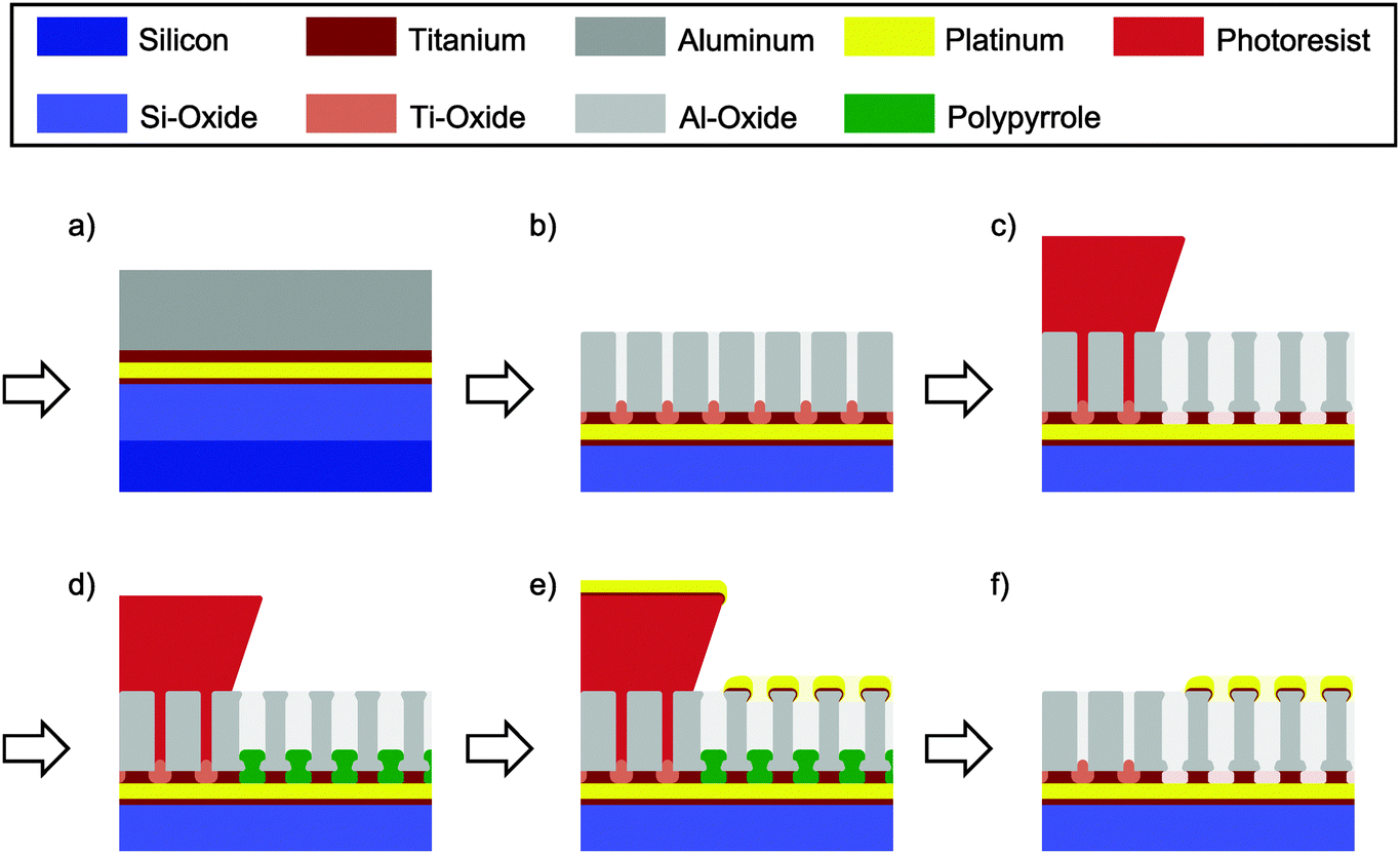 | ||
| Fig. 1 Key steps in the fabrication process of the nanoporous alumina sensor. After the initial layer deposition (a) the aluminum is anodized (b) resulting in alumina pores (light grey), which end in TiO2-plugs (light brown). All pores not protected by a photoresist (red) are subsequently opened and widened in a wet etch (c). The electrode (yellow) at the pore bottom is then again selectively encapsulated (d) by electrodepositing an insulating polymer (green). After the evaporation (e) of the top electrode (yellow) pyrrole and the resist are removed yielding the final sensing area (f, right). Porous parts not covered by a photoresist are neither opened nor widened and function as passivation for the bottom electrode's feed line (f, left). | ||
Electrochemical characterization
The cyclic voltammograms are recorded using a multi-potentiostat (1030b, CH Instruments Inc.) in a 3 M KCl electrolyte containing 330 μM K3[Fe(CN)6]. During the measurements a platinum wire serves as a counter electrode. A housed Ag/AgCl electrode (BASi Inc.) is used as a reference electrode. Using eutectic GaIn the top electrode is brought into contact with a probe needle from above while the bottom electrode is brought into contact at the cutting edge of the chip. Sweep rates of 20 mV s−1 and potential steps of 2 mV are chosen, corresponding to sampling rates of 10 Hz. The scanned potential window reaches from 50 mV to 650 mV vs. Ag/AgCl. The potential of the non-sweeping electrode is held at either reducing (50 mV) or oxidizing (650 mV) potential. Starting from 50 mV at least three sweeps are performed and the third sweep is presented. Prior to use the electrodes were swept multiple times to reach a constant current response.Numerical simulations
The numerical calculations were carried out in COMSOL 4.2 using the “transport of dilute species” package. The diffusive behavior within the volume is given by Fick's laws. Diffusion coefficients are assumed to be Dred = 6.32 × 10⁻⁶ cm2 s−1 and Dox = 7.63 × 10⁻⁶ cm2 s−1 for the reduced and the oxidized species,52 respectively. The initial concentrations of both species are given by cred = 300 μM and cox = 0 μM. At the electrodes the flux is defined via the Butler–Volmer-Equation. The transfer characteristics within the 3 M KCl electrolyte are approximated by a transfer rate of k = 8.5 × 10⁻² cm s−1,53 a transfer coefficient of α = 0.5 and a redox potential of E0 = 350 mV vs. Ag/AgCl. The sensor geometry is reduced to one radially symmetric pore in a cylindrical element, which is known as the diffusion domain approach.54–56 The basal area of domains with a radius of rvol = 45 nm is given by the total area of the sensor divided by the approximate number of pores. Above the pore a reservoir with a height of 400 μm is simulated. Two potential sweeps with the experimental rate of 20 mV s−1 are simulated; the concentration distribution of the second one is presented.Results and discussion
Sensor fabrication
The fabrication process of the nanoporous dual-electrode sensor is divided into three basic stages. As we can see from Fig. 1, these stages include the deposition of the Ti/Pt bottom electrode and an additional Ti/Al film (Fig. 1a), the generation of a porous insulating spacer from the Ti/Al layer (Fig. 1b and c) and the deposition of the Ti/Pt top electrode (Fig. 1d and e). Finally, we obtain a sensor at which the bottom electrode is separated from a porous top electrode by an equally porous insulating layer (Fig. 1f, right). The basic phases are sub-divided to include three key steps, which are particularly developed to enable the production of a large-area dual-electrode sensor.The first step involves the deposition of aluminum film (Fig. 1a) and its subsequent anodization yielding a nanoporous insulating alumina spacer (Fig. 1b). Beneath this film two layers of 10 nm Ti are deposited on top of the platinum bottom electrode. These layers fulfill a crucial task: in sum, they operate as a barrier layer to hinder the pores formed in the aluminum film during anodization to break through to the underlying platinum electrode and cause electrolysis and corrosion. At certain material interfaces anodization reactions are known to come to a halt.41 As alumina pores reach titanium, for instance, no titania pores are formed under the given anodization conditions.57–59 Instead, the oxidizing titanium expands into the alumina pores and seals, in our case, the platinum/electrolyte interface with titania plugs. To obtain a homogeneous termination of the anodization as well as an optimal adhesion of the formed layer stack each of the heterogeneous interfaces of the titanium layer (Pt/Ti and Ti/Al) are preferably evaporated within the same fabrication process.
Following the anodization process, the titanium oxide plugs, which have grown into the pores, have to be removed (Fig. 1c). Electrical51 or electrochemical50 processes are not applied as they are assumed to primarily facilitate the barrier removal at points with reduced trans-barrier resistance. Geometrical inhomogeneities at the titania/alumina interface might thus be increased. Using potentials beyond the electrochemical window of water, these processes can further lead to electrolysis and sample destruction.60 Consequently, a chemical etch for the selective removal of titanium oxide versus alumina has previously been reported.24,59 However, the wafer cleaning solution (SC-1) consisting of a slightly diluted mixture of H2O2 and NH4OH has also shown an insufficient homogeneity along large areas of structured layer stacks. Indicated by early bubble formation, especially the titania removal at the edges of the underlying electrode is found to progress faster than at the electrode centers.
Interestingly, we find a wide range of slightly acidic ammonia- and fluoride-free solutions perfectly suiting our needs as demonstrated in the SEM images of Fig. 2. A simple, two component etchant is given by an aqueous solution of 30 wt% hydrogen peroxide containing 0.35 M HEPES buffer. Applying the etch at elevated temperature (50 °C), the titania at the pores is removed and the alumina pores are slightly widened within one step (Fig. 2d). Aiming for a higher selectivity the perfect candidate is a mixture of 30 wt% hydrogen peroxide holding 0.05 M of EDTA. Adding, for instance, 0.35 M of sodium acetate further decreases the etching time to about 50 min while increasing the pH of the solution (pH ∼ 4). As we can see in Fig. 2a this new etching solution does not visibly attack the aluminum oxide, but it reliably etches the titania plugs. If, in contrast, widening of the pores is preferred oxalic acid can be added to any of the above solutions to gradually reduce the selectivity. The result for a peroxide-acetate-EDTA (PAcE) etching solution containing 0.15 M of oxalic acid is shown in Fig. 2b. Adding oxalic acid to the HEPES solution yields even wider pores (Fig. 2e). This tunable selectivity easily enables a defined control of the final diameter of the pores parallel to the pore opening.
 | ||
| Fig. 2 The effect of different etching solutions (a–e) used for titania-plug removal on the final pore width of the nanoporous alumina samples. Upper pictures show top views recorded via scanning electron microscopy and the lower row depicts breaking edges (60° angle). Pores with radii reaching from below 10 nm up to 25 nm can easily be obtained. HEPES samples (d and e) were fabricated starting from 300 nm aluminum films; for all other samples 200 nm aluminum was used. | ||
Instead of acetate also a phosphate buffer can be used to obtain a titania etch. As we can see in Fig. 2c for a 0.2 M K2POH4-solution, the phosphate etch again offers a lower selectivity versus alumina, even when being used without oxalic acid. As a widening of pores is desired, the electrochemical results presented here are derived from phosphate etched pores. In any case, a freshly prepared solution is used. With the ongoing decomposition of peroxide a decreased etching speed is observed for solutions being older than a few hours. Approximately 10 min after the first homogeneous occurrence of bubbles on top of the conducting paths the successful plug removal is finally indicated by a fast release of small bubbles, which might be interpreted as foaming.
Prior to the evaporation of the top electrode onto the alumina film the organic compound pyrrole is electrochemically deposited onto the bottom platinum layer (Fig. 1d). Due to a simultaneous over-oxidation in a slightly basic NaHCO3 solution61,62 (pH ∼ 9) we obtain an encapsulating polypyrrole (PPy) layer at all parts of the lower electrode facing the electrolyte. This includes the alumina pore bottom as well as possible defect spots. Shortcuts between the bottom electrode and the evaporated top electrode are thus prevented. The film growth is limited by the layer's increasing resistivity and the simultaneously decreasing interface potential at the PPy/electrolyte boundary. At the end of the deposition process the current across the PPy-film is found to be about 4 μA cm−2 at 1 V vs. Ag/AgCl. From a fabricated Pt–PPy–Pt stack (Fig. 3) we derive a layer thickness of 40 nm. Beneficial for the sensor fabrication, the films mechanical integrity is not affected by 3 min exposure to ethanol, isopropanol, acetone and DMSO. Cyclic voltammograms between the platinum layers of a Pt–PPy–Pt stack reveal currents that are growing exponentially up to several micro-amperes per square centimeter at 1 V potential difference. Therefore, the resistivity of layers is comparable to the one during deposition.
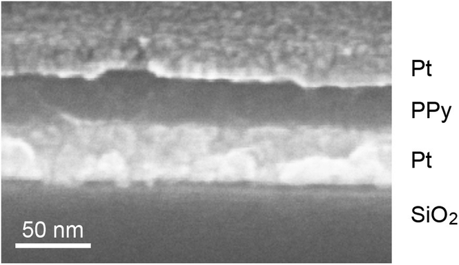 | ||
| Fig. 3 A Pt–PPy–Pt stack used to define the thickness of the deposited polypyrrole and its electrical isolation characteristics. Within the alumina template the PPy encapsulation reaches a comparable height. | ||
After the metallization process (Fig. 1e) polypyrrole not being covered by the deposited platinum can quickly be removed by oxygen plasma at a pressure of 0.3 mbar within about 5 min (Fig. 1f). In contrast, polypyrrole enclosed between top and bottom electrodes at defect spots is not removed and functions as a simple insulating spacer between the electrodes. Porous parts of the wafer that have been covered with photoresist after the anodization process are electrically inactive. On the one hand, the metal stack evaporated to form the top electrode is removed via lift off. On the other hand, the bottom electrode is isolated from the electrolyte by the alumina layer and the titania plugs terminating the 40 V anodization process.
Sensor layout
The final sensor is presented in Fig. 4. As we can see from the photograph in Fig. 4a the layout of the 11 × 11 mm2 chip can be divided into four basic zones. Areas holding the bare SiO2–TiOx–AlOx stack appear dark red. The top electrode, which is deposited onto widened pores, is metallic grey in color. The feed lines of the bottom electrode, covered by non-widened alumina pores sealed by titania plugs, appear in a pink color. At the central 3 × 3 mm2 crossing area, which is surrounded by a glass ring, the pores are widened and opened towards the underlying bottom electrode. A closer look at the pore geometry is given in Fig. 4b by scanning electron microscopy (SEM) recordings of focused ion beam (FIB) cut sections at the active sensor site. The pores unveil the typical geometry of the sensor's nanopores. Top and bottom electrodes can be clearly identified by their bright appearance. In between we find the porous alumina spacer. The central part of a pore features a width of about 20 nm. At their top, the pores tend to feature radii of about 10 nm. Depending on the specific pore the narrowing is the result of tapering of the alumina pores itself or the consequence of a protruding top electrode. Also at the lower 30 nm of a pore the radius roughly amounts to 10 nm. Beneath this narrowed part and right above the platinum bottom electrode we again find a wider region, which originates from the titania plug removal. This gap is identified more easily by breaking edges similar to those in Fig. 2.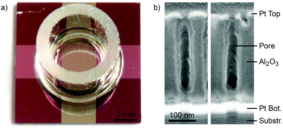 | ||
| Fig. 4 A photograph (a) of the crossbar sensor shows the lateral arrangement of the bottom electrode (pink, left to right) and top electrode (grey, top to bottom) of 3 mm width. The crossing area (center) is surrounded by a glass ring glued onto the chip. The central sensing site is investigated more closely by scanning electron imaging of focused ion beam cuts (b). Here, top and bottom electrodes can be identified by their bright appearance. The cutting edge's normal is tilted downwards by 38° relatively to the direction of view. | ||
Sensitivity
The nanoporous sensor is characterized by performing voltammetric sweeps of the sensor electrodes in an aqueous 3 M KCl electrolyte containing 330 μM K3Fe(CN)6. Due to the high KCl concentrations, the electric potential at any sensor surface is shielded by the electric double layer within the sub-nanometer range. Purely driven by diffusive motion, the redox-active K3Fe(CN)6-analyte can shuttle freely between the electrodes as well as between pores and the reservoir. While the top (red) or the bottom (blue) electrode is swept, the opposing electrode is held at a reducing potential of 50 mV (Fig. 5a) or at an oxidizing potential of 650 mV (Fig. 5b) vs. Ag/AgCl. As we can see, no currents between both electrodes are detected for similar overpotentials. As the sweeping electrode potential approaches the redox potential close to E0 = 350 mV the detected top (solid line) and bottom (dashed line) currents increase in a step like manner. Induced by redox-cycling Fe(CN)63+/4+-ions a current of about 100 μA is reached at maximally opposing overpotentials. Simultaneously, the intrinsic conductivity between top and bottom electrodes amounts to only 150 nA and is therefore negligible.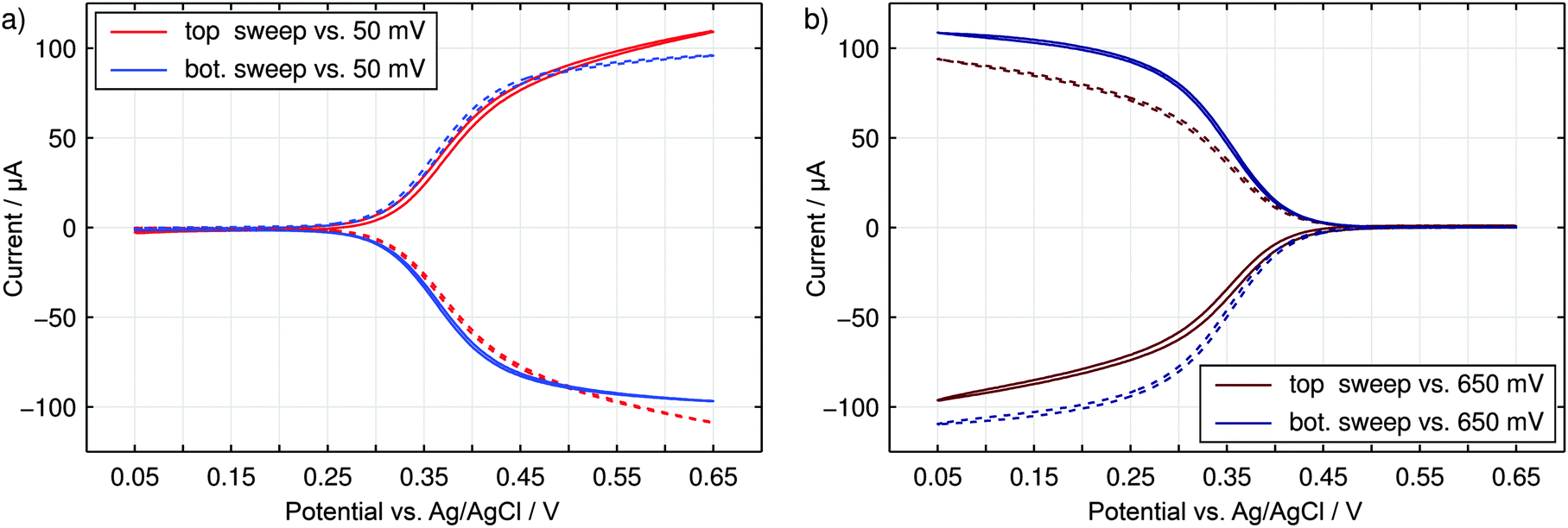 | ||
| Fig. 5 Cyclic voltammograms obtained for 330 μM K3[Fe(CN)6] in a 3 M KCl supporting electrolyte. Either the top electrode (red) or the bottom electrode (blue) is swept over the depicted potential range. The opposing electrode is set to a constant reducing (a) or oxidizing (b) potential. Top (solid) and bottom (dashed) currents are shown. | ||
Consequently, the fabricated sensor offers good sensing qualities with a unique sensitivity of up to 330 μA mM−1. This sensitivity is equal to a signal amplification of approximately 730× compared to the steady state current of single disk electrodes with an identical basal area.63,64 Also the redox-cycling sensitivities reported in literature are exceeded by at least two orders of magnitude. Primarily due to their smaller dimensions they lie in the range of 100 nA mM−1 to 1 μA mM−1.21,28,31 But even the per-area sensitivity of 3.6 mA mM−1 cm−2 of the presented sensor is situated at the upper end of pore-based approaches.
The analyte exchange between top and bottom electrodes and thus the signal magnitude both benefit from the dense packing of the nanopores in the alumina membrane. Aiming at optimized sensitivities, wider pores can be obtained by the addition of oxalic acid to the plug-removal solution. Wafers etched with the highly selective oxalate-free acetate solution (PAcE) yield sensors holding pore diameters in the low nanometer range. With values around 0.1 mA mM−1 cm−2 they consequently show the lowest per-area sensitivities of all sensors fabricated. When, in contrast, carrying out an extended pore widening with, for instance, HEPES and oxalate containing peroxide-etch simulations suggest that sensitivities of up to 10.0 mA mM−1 cm−2 could be reached.
Macro-electrode impact on nano-electrochemistry
Comparing the current maxima of the two sweep configurations (Fig. 5) we observe a difference of about 11%. As numerical simulations show, this disparity is a direct result of the distinct diffusion coefficients of the reduced and oxidized species of the Fe(CN)63+/4+ redox couple. An exemplary view of the analyte concentration is given in Fig. 6 for maximally opposing overpotentials. The analyte is considered to initially contain only reduced molecules. Thus, setting the upper electrode to a reducing potential (Fig. 6a), composition and concentration at the electrode remain unaltered. At the lower electrode, in contrast, the molecules are converted to the more mobile oxidized species. As the higher mobility implies an increased chance of escaping the generating electrode, the absolute number of molecules at the pore bottom is decreased. A similar behavior can be observed at an oxidizing top electrode and its adjacent reservoir (Fig. 6b). In general, we find the concentrations at the macroscopic top electrode to follow the behavior of a single electrode that is coupled to a quasi-infinite reservoir via planar diffusion.65 Interestingly, the effects of the concentrations at the bottom electrode differ from those at the pore's top. While the concentration at the pore's top changes by only (Dox/Dred)1/2, the bottom concentration varies by a factor of (Dred/Dox)3/2 upon inversion of the electrode potentials. This fact is to be attributed to the quasi-steady state within the pores. As a consequence, the amount of analyte at the lower electrode is linked to the concentration at the upper electrode66 rather than to the bulk concentration. Solely depending on the overpotential configuration, the correlation is given by cbotsum = Dox/Dred × ctopsum for an oxidizing top and a reducing bottom electrode or by cbotsum = Dred/Dox × ctopsum for the inverse case.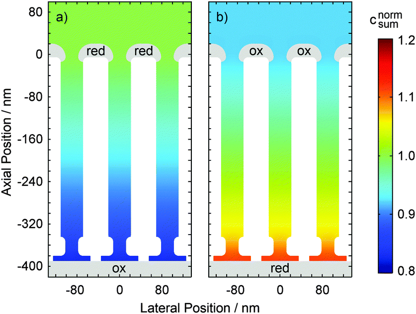 | ||
| Fig. 6 Normalized distribution of the overall analyte concentration csum in a nanoporous sensor undergoing planar diffusion. Just like the currents in Fig. 5 the average concentrations within the pores are lower in the case of a top electrode being biased to 50 mV and a bottom electrode biased to 650 mV (a) than for the inverse configuration (b). Note that distinct diffusion constants for reduced and oxidized species are used (Dred = 6.32 × 10⁻⁶ cm2 s−1 and Dox = 7.63 × 10⁻⁶ cm2 s−1). | ||
In our specific case, analyte molecules cycling between the electrodes mainly react at the lower part of the top electrode. Consequently, the presented sensor can be depicted as a separately acting planar electrode and a nanocavity redox cycling device, which are interlinked only via diffusion through the porous top electrode. Due to the coupling, the absolute number of molecules participating in inner-porous redox cycling depends on the potential configuration. In agreement with the average concentration in the pores we deduce the ratio of the regarding currents at maximum overpotentials to be:
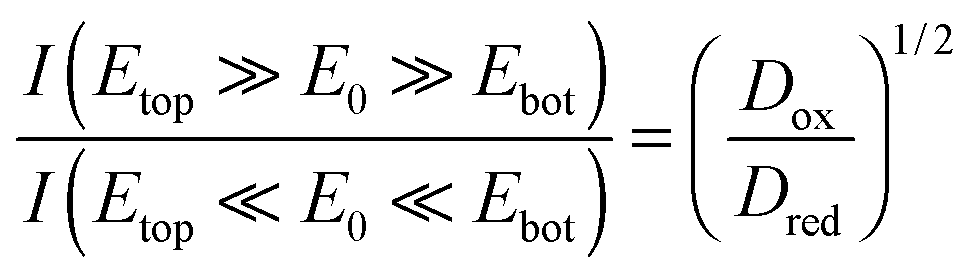
This equation is a result of the unique interplay of the specific geometry of hundreds of millions of pores being densely integrated on a sensor array of millimeter dimensions. For smaller devices or sensors with symmetrically arranged electrodes the redox-cycling currents I(Etop ≫ E0 ≫ Ebot) and I(Etop ≪ E0 ≪ Ebot) are identical.31,66 Despite fundamental differences in the electrode layout, configuration-dependent currents have been reported for off-chip approaches using SECM in the vicinity of biased macroelectrodes.67 The data shown in Fig. 5, in contrast, represent the first on-chip observation of a corresponding effect.
As we can see from the above equation, the ratio of the currents at maximum opposing overpotentials is directly connected to the ratio γ = Dox/Dred. Furthermore, the current ratio is independent of other parameters, such as the amount of reduced and oxidized species in the bulk electrolyte. Consequently, the introduced nanoporous sensor provides a convenient way for the determination of the analyte's species dependent diffusion coefficients. When calculating the ratio of the diffusion constants from the experimental currents at ±300 mV we obtain γ = 1.24. As kinetic effects are still notable at the chosen maximum overpotential, this presented result might be associated with some experimental uncertainties. The derived value, however, clearly reflects the high mobility of the oxidized Fe(CN)63− ion. It is further in perfect agreement with the values Dox/Dred = 1.19–1.24 expected from the data available for 2 M KCl solutions.52,68
To induce a redox-cycling state fully limited by diffusion, higher overpotentials could be applied. Alternatively, the electrode spacing can be enlarged. Starting with aluminum films of higher thickness the alumina sensor approach offers the opportunity to obtain pores with very high aspect ratios. Retaining the pore specific layout, even the diffusive behavior of redox-couples with slow or highly asymmetric transfer kinetics could thus be investigated.
Conclusions
We presented the fabrication and application of a nanoporous electrochemical sensor. Our method employs on-chip integration of dual-electrode structures separated by nanoporous alumina films. The sensors make use of very efficient redox cycling amplification inside the nanopores and demonstrate high and reliable sensitivities during detection of redox-active analytes. Specific geometric aspects of the sensor further reveal the dependence of the molecule's diffusion coefficient on the oxidation state.The geometrical pore characteristics can easily be adapted to the experimental requirements. Titanium oxide etching solutions with a tunable selectivity versus alumina allow fabrication of pores with variable width. Additionally, a method for the selective deposition of a protecting layer onto nanopatterned electrode areas was introduced. This technique is not restricted to the use of alumina templates. It might more generally be applied to form permanent or reversible encapsulation of micro- or nanostructured electrodes. The presented techniques enable the high-throughput fabrication of nanoporous dual-electrode structures on the wafer-scale.
Finally, the highly parallelized fabrication and the needlessness of expensive patterning techniques might initiate a breakthrough of sensitive redox cycling sensors in a wide range of applications. For instance, the introduced concept might soon be utilized to locally detect neurotransmitters that are released by biological networks for intercellular communication.
Acknowledgements
We thank Marko Banzet, Hans Wingens and Dieter Strobl for their support regarding fabrication and hardware as well as Philipp Rinklin and Alexandre Kisner for helpful discussions on the project. We gratefully acknowledge funding by the Helmholtz Young Investigator Program.Notes and references
- L. B. Anderson and C. N. Reilley, J. Electroanal. Chem., 1965, 10, 295–305 CAS.
- E. Kätelhön and B. Wolfrum, Rev. Anal. Chem., 2012, 31, 7–14 CrossRef.
- E. O. Barnes, G. E. M. Lewis, S. E. C. Dale, F. Marken and R. G. Compton, Analyst, 2012, 137, 1068–1081 RSC.
- M. Yokokawa, D. Itoh and H. Suzuki, in Applications of Nanomaterials in Sensors and Diagnostics, ed. A. Tuantranont, Springer Berlin Heidelberg, 2013, pp. 257–279 Search PubMed.
- J. O. Howell and R. M. Wightman, Anal. Chem., 1984, 56, 524–529 CrossRef CAS.
- R. D. Lama, K. Charlson, A. Anantharam and P. Hashemi, Anal. Chem., 2012, 84, 8096–8101 CrossRef CAS PubMed.
- A. J. Bard, F. R. F. Fan, J. Kwak and O. Lev, Anal. Chem., 1989, 61, 132–138 CrossRef CAS.
- M. A. Edwards, S. Martin, A. L. Whitworth, J. V. Macpherson and P. R. Unwin, Physiol. Meas., 2006, 27, R63 CrossRef PubMed.
- A. Schulte and W. Schuhmann, Angew. Chem., Int. Ed., 2007, 46, 8760–8777 CrossRef CAS PubMed.
- D. G. Sanderson and L. B. Anderson, Anal. Chem., 1985, 57, 2388–2393 CrossRef CAS.
- K. Aoki, M. Morita, O. Niwa and H. Tabei, J. Electroanal. Chem. Interfacial Electrochem., 1988, 256, 269–282 CrossRef CAS.
- Y. Liu, B. Wolfrum, M. Hüske, A. Offenhäusser, E. Wang and D. Mayer, Angew. Chem., Int. Ed., 2013, 52, 4029–4032 CrossRef CAS PubMed.
- F. J. del Campo, L. Abad, X. Illa, E. Prats-Alfonso, X. Borrisé, J. M. Cirera, H.-Y. Bai and Y.-C. Tsai, Sens. Actuators, B, 2014, 194, 86–95 CrossRef CAS PubMed.
- M. A. G. Zevenbergen, D. Krapf, M. R. Zuiddam and S. G. Lemay, Nano Lett., 2007, 7, 384–388 CrossRef CAS PubMed.
- B. Wolfrum, M. Zevenbergen and S. Lemay, Anal. Chem., 2008, 80, 972–977 CrossRef CAS PubMed.
- E. Kätelhön, B. Hofmann, S. G. Lemay, M. A. G. Zevenbergen, A. Offenhäusser and B. Wolfrum, Anal. Chem., 2010, 82, 8502–8509 CrossRef PubMed.
- Y. Lim, J.-I. Heo and H. Shin, Sens. Actuators, B, 2014, 192, 796–803 CrossRef CAS PubMed.
- C. S. Henry and I. Fritsch, Anal. Chem., 1999, 71, 550–556 CrossRef CAS PubMed.
- C. S. Henry and I. Fritsch, J. Electrochem. Soc., 1999, 146, 3367–3373 CrossRef CAS PubMed.
- S. Neugebauer, U. Müller, T. Lohmüller, J. P. Spatz, M. Stelzle and W. Schuhmann, Electroanalysis, 2006, 18, 1929–1936 CrossRef CAS.
- T. Lohmüller, U. Müller, S. Breisch, W. Nisch, R. Rudorf, W. Schuhmann, S. Neugebauer, M. Kaczor, S. Linke, S. Lechner, J. Spatz and M. Stelzle, J. Micromech. Microeng., 2008, 18, 115011 CrossRef.
- D. Menshykau, A. M. O'Mahony, F. J. del Campo, F. X. Munõz and R. G. Compton, Anal. Chem., 2009, 81, 9372–9382 CrossRef CAS PubMed.
- S.-J. Li, J. Li, K. Wang, C. Wang, J.-J. Xu, H.-Y. Chen, X.-H. Xia and Q. Huo, ACS Nano, 2010, 4, 6417–6424 CrossRef CAS PubMed.
- M. Hüske and B. Wolfrum, Phys. Status Solidi A, 2011, 208, 1265–1269 CrossRef.
- F. Zhu, J. Yan, M. Lu, Y. Zhou, Y. Yang and B. Mao, Electrochim. Acta, 2011, 56, 8101–8107 CrossRef CAS PubMed.
- S. P. Branagan, N. M. Contento and P. W. Bohn, J. Am. Chem. Soc., 2012, 134, 8617–8624 CrossRef CAS PubMed.
- L. R. Gibson, S. P. Branagan and P. W. Bohn, Small, 2013, 9, 90–97 CrossRef CAS PubMed.
- C. Ma, N. M. Contento, L. R. Gibson and P. W. Bohn, ACS Nano, 2013, 7, 5483–5490 CrossRef CAS PubMed.
- C. Ma, N. M. Contento, L. R. Gibson and P. W. Bohn, Anal. Chem., 2013, 85, 9882–9888 CrossRef CAS PubMed.
- A. Oleinick, F. Zhu, J. Yan, B. Mao, I. Svir and C. Amatore, ChemPhysChem, 2013, 14, 1887–1898 CrossRef CAS PubMed.
- M. Hüske, R. Stockmann, A. Offenhäusser and B. Wolfrum, Nanoscale, 2014, 6, 589–598 RSC.
- V. A. T. Dam, W. Olthuis and A. van den Berg, Analyst, 2007, 132, 365–370 RSC.
- M. J. J. van Megen, M. Odijk, J. Wiedemair, W. Olthuis and A. van den Berg, J. Electroanal. Chem., 2012, 681, 6–10 CrossRef CAS PubMed.
- W. Miao, Z. Ding and A. J. Bard, J. Phys. Chem. B, 2002, 106, 1392–1398 CrossRef CAS.
- P. Sun and M. V. Mirkin, Anal. Chem., 2006, 78, 6526–6534 CrossRef CAS PubMed.
- A. de la Escosura-Muñiz and A. Merkoçi, Electrochem. Commun., 2010, 12, 859–863 CrossRef PubMed.
- Z. P. Aguilar, W. R. Vandaveer and I. Fritsch, Anal. Chem., 2002, 74, 3321–3329 CrossRef CAS.
- S. Neugebauer, L. Stoica, D. Guschin and W. Schuhmann, Microchim. Acta, 2008, 163, 33–40 CrossRef CAS.
- A. Ghicov and P. Schmuki, Chem. Commun., 2009, 2791–2808 RSC.
- S. P. Albu, A. Ghicov, S. Aldabergenova, P. Drechsel, D. LeClere, G. E. Thompson, J. M. Macak and P. Schmuki, Adv. Mater., 2008, 20, 4135–4139 CAS.
- Y. Lei, W. Cai and G. Wilde, Prog. Mater. Sci., 2007, 52, 465–539 CrossRef CAS PubMed.
- A.-P. Li, F. Müller, A. Birner, K. Nielsch and U. Gösele, Adv. Mater., 1999, 11, 483–487 CrossRef CAS.
- G. D. Sulka, in Nanostructured Materials in Electrochemistry, ed. A. Eftekhari, Wiley-VCH Verlag GmbH & Co. KGaA, 2008, pp. 1–116 Search PubMed.
- G. D. Sulka and W. J. Stepniowski, Electrochim. Acta, 2009, 54, 3683–3691 CrossRef CAS PubMed.
- H. Masuda, K. Yada and A. Osaka, Jpn. J. Appl. Phys., 1998, 37, L1340–L1342 CrossRef.
- S. Ono and N. Masuko, Surf. Coat. Technol., 2003, 169–170, 139–142 CrossRef CAS.
- W. Lee, R. Ji, U. Gosele and K. Nielsch, Nat. Mater., 2006, 5, 741–747 CrossRef CAS PubMed.
- X. Wang and S. Smirnov, ACS Nano, 2009, 3, 1004–1010 CrossRef CAS PubMed.
- T. R. B. Foong, A. Sellinger and X. Hu, ACS Nano, 2008, 2, 2250–2256 CrossRef CAS PubMed.
- O. Rabin, P. R. Herz, Y. M. Lin, A. I. Akinwande, S. B. Cronin and M. S. Dresselhaus, Adv. Funct. Mater., 2003, 13, 631–638 CrossRef CAS.
- M. M. Crouse, A. E. Miller, D. T. Crouse and A. A. Ikram, J. Electrochem. Soc., 2005, 152, D167 CrossRef CAS PubMed.
- M. V. Stackelberg, M. Pilgram and V. Toome, Z. Elektrochem. Angew. Phys. Chem., 1953, 57, 342–350 CAS.
- J. Kůta and E. Yeager, J. Electroanal. Chem. Interfacial Electrochem., 1975, 59, 110–112 CrossRef.
- H. Reller, F. Kirowa-Eisner and E. Gileadi, J. Electroanal. Chem. Interfacial Electrochem., 1982, 138, 65–77 CrossRef CAS.
- C. Amatore, J. M. Savéant and D. Tessier, J. Electroanal. Chem. Interfacial Electrochem., 1983, 147, 39–51 CrossRef CAS.
- F. G. Chevallier, L. Jiang, T. G. J. Jones and R. G. Compton, J. Electroanal. Chem., 2006, 587, 254–262 CrossRef CAS PubMed.
- S.-Z. Chu, S. Inoue, K. Wada, S. Hishita and K. Kurashima, Adv. Funct. Mater., 2005, 15, 1343–1349 CrossRef CAS.
- H. Tsuchiya, S. Berger, J. M. Macak, A. Ghicov and P. Schmuki, Electrochem. Commun., 2007, 9, 2397–2402 CrossRef CAS PubMed.
- S.-H. Park, S. Kim, D.-J. Lee, S. Yun, Z. G. Khim and K.-B. Kim, J. Electrochem. Soc., 2009, 156, K181–K185 CrossRef CAS PubMed.
- N. Tasaltin, S. Öztürk, N. Kilinç, H. Yüzer and Z. Öztürk, Appl. Phys. A: Mater. Sci. Process., 2009, 95, 781–787 CrossRef CAS.
- T. Osaka, T. Momma and H. Kanagawa, Chem. Lett., 1993, 649–652 CrossRef CAS.
- T. Osaka, T. Momma, S. Komaba, H. Kanagawa and S. Nakamura, J. Electroanal. Chem., 1994, 372, 201–207 CrossRef CAS.
- K. Aoki and J. Osteryoung, J. Electroanal. Chem. Interfacial Electrochem., 1981, 122, 19–35 CrossRef CAS.
- D. Shoup and A. Szabo, J. Electroanal. Chem. Interfacial Electrochem., 1982, 140, 237–245 CrossRef CAS.
- R. D. Martin and P. R. Unwin, J. Electroanal. Chem., 1997, 439, 123–136 CrossRef CAS.
- D. Mampallil, K. Mathwig, S. Kang and S. G. Lemay, Anal. Chem., 2013, 85, 6053–6058 CrossRef CAS PubMed.
- R. D. Martin and P. R. Unwin, Anal. Chem., 1998, 70, 276–284 CrossRef CAS.
- G. Gerhardt and R. N. Adams, Anal. Chem., 1982, 54, 2618–2620 CrossRef CAS.
Footnote |
| † Electronic supplementary information (ESI) available. See DOI: 10.1039/c4cp01027b |
| This journal is © the Owner Societies 2014 |