 Open Access Article
Creative Commons Attribution 3.0 Unported Licence
Nanostructured electrochromic smart windows: traditional materials and NIR-selective plasmonic nanocrystals
Evan L.
Runnerstrom
ab,
Anna
Llordés
a,
Sebastien D.
Lounis
ac and
Delia J.
Milliron
*ad
aThe Molecular Foundry, Lawrence Berkeley National Laboratory, 1 Cyclotron Rd., Berkeley, CA 94720, USA
bDepartment of Materials Science and Engineering, The University of California, Berkeley, CA 94720, USA
cGraduate Group in Applied Science and Technology, The University of California, Berkeley, CA 94720, USA
dDepartment of Chemical Engineering, The University of Texas at Austin, 200 E. Dean Keeton St., Austin, TX 78712, USA. E-mail: milliron@che.texas.edu
First published on 4th June 2014
Abstract
Electrochromic devices, which dynamically change colour under applied potential, are widely studied for use in energy-efficient smart windows. To improve the viability of smart windows, many researchers are utilizing nanomaterials, which can provide electrochromic devices with improved colouration efficiencies, faster switching times, longer cycle lives, and potentially reduced costs. In an effort to demonstrate a new type of electrochromic device that goes beyond the capabilities of commonly used electrochromic materials, researchers have turned to plasmonic transparent conductive oxide (TCO) nanocrystals. Electrochemical injection of electrons into plasmonic TCO nanocrystal films induces a shift in the plasmon frequency and gives rise to the new functionality of selective optical modulation in the near-infrared region of the solar spectrum. These nanocrystals can be used as building blocks to enable creation of advanced electrochromic devices containing mesoporous electrodes or nanocrystal-in-glass composites. Such devices have been important in advancing the field towards achieving the ideal smart window with independent control over visible and NIR transmittance.
1. Introduction
Electrochromism, the phenomenon whereby a material's colour, transparency, or other optical property changes in response to electric charge, forms the basis for operation of a number of devices, including displays, adjustable mirrors, and “smart” windows. While reversible colour changes in inorganic materials have been studied at least since the discovery of tungsten bronzes in the 19th century,1,2 Deb's demonstration of reversible, electrically induced colouration in thin films of transition metal oxides in the late 1960s and 1970s launched significant efforts to study electrochromic materials and devices for applications like displays and mirrors.3,4 Motivated by the potential for significant energy savings from reduced cooling and heating loads, the research in this area has shifted towards developing electrochromic windows that dynamically control sunlight entering a building.1,2,5–9 This focus on improved energy efficiency and the development of advanced buildings drives the majority of current electrochromic research.An ideal smart window, universally applicable across building types and climate zones, would independently control the transmittance of visible sunlight and solar heat into a building. These two parameters directly affect a building's energy use and influence occupant comfort. For this reason, independent control over the visible and near-infrared (NIR) regions of the solar spectrum is a key target for advanced electrochromic devices, and would contribute to optimum energy efficiency across a building's heating, cooling, and artificial lighting systems. NIR light, in particular, accounts for about half of the solar energy that is incident upon a window (Fig. 1a), but does not contribute to daylighting within a building. An optimized electrochromic window would thus provide separate, dynamic control over the transmission of visible and NIR solar radiation using materials with high optical contrast, fast switching times, long cycle life, and low manufacturing cost.
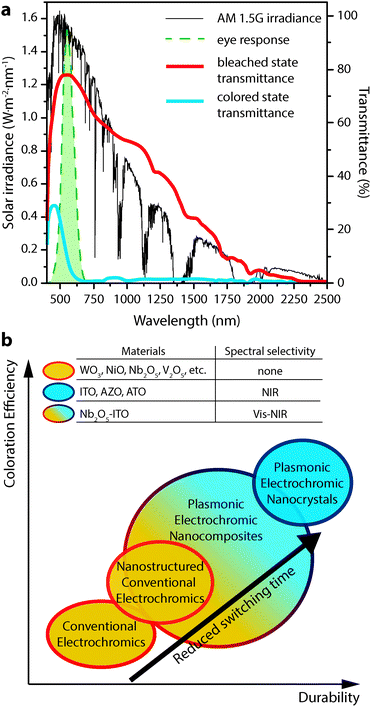 | ||
| Fig. 1 (a) AM 1.5G solar spectrum (thin black curve) along with the photopic response of the human eye (dashed green curve). Overlaid are the transmittance curves for a commercial electrochromic device (Gesimat) in the bleached (thick red curve) and coloured (thick blue curve) states. Note the significant modulation of both visible and NIR light. (b) Scheme illustrating the performance metrics achieved by the different classes of electrochromic materials discussed in this review. Transmittance curves in panel (a) reproduced from ref. 12, copyright 2009, with permission from Elsevier. | ||
Unfortunately, the benefits of electrochromic windows are yet to be realized at scale,6 as conventional materials suffer from significant drawbacks related to cost, durability, and functionality. Existing commercial electrochromic windows most often employ thin films of transition metal oxides as the active material.2,9,10 These films are typically grown using costly physical vapour processes such as sputtering or evaporation,5–7,9 suffer from material degradation associated with repeated ion intercalation,6,7,9,10 and adopt dark, distinct colours in their tinted states,2,9,11 simultaneously blocking both visible and NIR light (Fig. 1a).12,13 For these reasons, conventional electrochromics fall short of the ideal smart window and have struggled to achieve widespread adoption.
In many cases, conventional inorganic electrochromic compounds in nanomaterial form exhibit enhanced properties, such as faster ON/OFF switching times and amenability to potentially low-cost solution processing. However, despite these advantages, nanostructuring does not necessarily confer new functionality. Films made from nanostructured transition metal oxide materials typically display similar optical properties to their bulk counterparts and miss the target of ideal solar control.
Our laboratory is spearheading the development of a new and fundamentally different class of electrochromic devices, leveraging the plasmonic properties of colloidal transparent conducting oxide (TCO) nanocrystals to directly address the aforementioned limitations of conventional materials.14–17 These nanocrystals exhibit strong localized surface plasmon resonance (LSPR) absorption in the mid- to near-IR. Electrochemical charging or doping of a nanocrystal film subsequently tunes the LSPR frequency over a wide range of wavelengths. Plasmonic nanocrystal electrochromic devices confer NIR-selective operation, inherently rapid switching, and greatly enhanced durability, and are made using solution processing. This review will cover in detail the scientific history and basis of NIR-selective plasmonic electrochromism and the devices that are enabled by this phenomenon. We will also provide a general overview of electrochromic device operation, briefly discuss conventional electrochromic materials, and consider a few other applications of nanotechnology to conventional electrochromic materials and devices. The relative electrochromic performance achieved by the materials discussed in this review—conventional materials, nanostructured conventional materials, plasmonic electrochromic nanocrystals, and composites of plasmonic nanocrystals in amorphous electrochromic glasses—is summarized schematically in Fig. 1b.
2. Fundamentals of electrochromic device operation
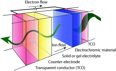
A typical electrochromic window coating, depicted in Fig. 2, is a multi-layer device consisting of an active electrochromic electrode layer, a counter electrode layer, an electrolyte layer separating the two electrodes, two transparent conducting layers serving as electrical leads, and the supporting substrates. The two electrode layers often consist of transition metal oxides. This device structure is referred to as “battery type” and is the most common geometry for electrochromic devices.5,7,9 In the off or bleached state, cations, such as Li+ or H+, reside in the electrolyte and the counter electrode.7 When the device is switched on, a voltage applied between the opposing conducting layers drives cations to migrate from the counter electrode, through the electrolyte, and into the electrochromic electrode through a Faradaic process, changing its oxidation state and its optical properties. For a thorough treatment of transition metal oxide electrochromic materials and counter electrodes, the reader is referred to a number of reviews and books.1,2,5–9,18–21An effective electrochromic device will have fast switching between its “on” and “off” states, good durability characterized by a long cycle life, and a high optical contrast ratio. These characteristics derive, in part, from the properties of the active electrochromic material. Many factors can influence switching speed, including the electronic conductivity of the electrode materials and the underlying conducting layers, the ionic conductivity of the electrolyte, the morphology of the electrochromic layer and the associated changes in ionic diffusion within that morphology, and ion insertion kinetics.8 Durability is typically quantified by measuring the changes in charge capacity or colouration efficiency over many thousands of electrochemical cycles. Assuming that a real-world electrochromic window undergoes one full cycle per day, a 30-year lifetime equates to a cycle life of about 11![[thin space (1/6-em)]](https://www.rsc.org/images/entities/char_2009.gif) 000. An emerging industry standard includes testing to at least 50
000. An emerging industry standard includes testing to at least 50![[thin space (1/6-em)]](https://www.rsc.org/images/entities/char_2009.gif) 000 cycles.
000 cycles.
To compare performance among different electrochromic materials and devices, researchers use the colouration efficiency as a key figure of merit. Colouration efficiency (CE) is given by:6,8
 | (1) |
3. Overview of current state-of-the-art conventional electrochromic materials
Here we briefly discuss the current state of the art in conventional inorganic electrochromic materials. Electrochromic properties of these materials and the plasmonic metal oxides, which are discussed later in the article, are summarized in Table 1.| Material/device | Electrochemical colouration mechanism | Absorption process | Spectral selectivity | Maximum CE | Switching speed | Cycle life |
|---|---|---|---|---|---|---|
| Amorphous WO3 | Ion insertion (cathodic)6 | Polaron absorption, charge transfer1,7 | VIS and NIR (coupled)7 | 50–80 cm2 C−1 (ref. 6 and 7) | Minutes | 10![[thin space (1/6-em)]](https://www.rsc.org/images/entities/char_2009.gif) 000 to 100 000 to 100![[thin space (1/6-em)]](https://www.rsc.org/images/entities/char_2009.gif) 000 (full devices)10 000 (full devices)10 |
| Crystalline WO3 | Ion intercalation (cathodic)7 | Polaron absorption, charge transfer, free carrier absorption1,6,7 | VIS and NIR (coupled) | 42 cm2 C−1 (ref. 22) | Minutes22 | >300022 |
| NiO | Pseudocapacitive (anodic)6,23 | Polaron absorption, charge transfer5,6 | VIS and NIR (coupled)5 | 30–100 cm2 C−1 (ref. 6 and 7) | 53 ms (nanostructured NiO)24 | 10![[thin space (1/6-em)]](https://www.rsc.org/images/entities/char_2009.gif) 000 to 100 000 to 100![[thin space (1/6-em)]](https://www.rsc.org/images/entities/char_2009.gif) 000 (full devices)10 000 (full devices)10 |
| ATO nanocrystals25 | Capacitive + insertion (cathodic) | Plasmon/free carrier absorption + charge transfer | Mid-IR, visible (independent) | 18 cm2 C−1 | 150 ms | >1![[thin space (1/6-em)]](https://www.rsc.org/images/entities/char_2009.gif) 000 000![[thin space (1/6-em)]](https://www.rsc.org/images/entities/char_2009.gif) 000 000 |
| ITO nanocrystals14,15 | Capacitive (cathodic) | Plasmon absorption | NIR only | 375 cm2 C−1 | 50 ms | 5000–20![[thin space (1/6-em)]](https://www.rsc.org/images/entities/char_2009.gif) 000 000 |
| AZO nanocrystals15 | Capacitive (cathodic) | Plasmon absorption | Mid-IR, NIR only | 400 cm2 C−1 | 60 ms | >20![[thin space (1/6-em)]](https://www.rsc.org/images/entities/char_2009.gif) 000 000 |
| ITO nanocrystals + NbOx glass16 | Capacitive + insertion (cathodic) | Plasmon absorption + polaron absorption | NIR and visible (independent) | 30 cm2 C−1 |
NIR mode: tens of ms
VIS mode: minutes |
>2000 |
| “Ideal” smart window | Capacitive (cathodic and anodic) | Plasmon absorption + polaron or charge transfer | NIR and visible (independent) | ∞ | Seconds or less | 50![[thin space (1/6-em)]](https://www.rsc.org/images/entities/char_2009.gif) 000 or greater 000 or greater |
Tungsten oxide (WO3) is the most widely studied electrochromic material. Upon cathodic Faradaic charge injection, WO3 changes colour from a clear, transparent state to a dark blue, translucent state as tungsten ions are reduced. Protons or alkali cations in the electrolyte compensate the injected electrons through insertion into WO3 octahedral sites, as shown by the following chemical and defect reactions:2
| yLi+ + ye− + W(VI)O3 ↔ LiyW(V)yW(VI)1−yO3 (blue) | (2) |
 | (3) |
The physical basis for the colouration is not completely understood,1 but the prevailing theory is that the injected electrons occupy the previously empty d band, giving rise to new electronic transitions. In crystalline WO3, the added electrons occupy delocalized states, while in amorphous WO3, they are localized at metal sites, resulting in polaronic absorption that can be described as an electronic charge-transfer transition between adjacent metal sites with different valency.1,6,7,9 In general, amorphous WO3 is considered to have the best overall performance among inorganic electrochromes, due to its high colouration efficiency of over 50 cm2 C−1, fast switching times, and good cycle life.6
The other well-studied transition metal oxides with cathodic colouration are TiO2, Nb2O5, MoO3, and Ta2O5.6,7,9 Like WO3, these oxides have edge- and corner-sharing MO6 octahedra within their crystal structure, which facilitates ion motion through the tunnels or chains of interstitial sites that form in periodic structures of these octahedra.7 They also share similar electronic band structures, with intrinsically empty d bands that become populated upon cathodic charge injection, inducing a colour change through new intraband transitions.9 Aside from WO3, however, cathodic metal oxides have generally proved disappointing due to factors like poor film durability against electrochemical cycling and low colouration efficiency.
Anodically colouring oxides are usually employed as a counter electrode that colours in a complementary fashion to the primary electrochromic electrode. The most popular of these is NiO, which is transparent in its lithiated or reduced state and gray in its oxidized state. NiO-based thin films have colouration efficiencies ranging from around 30 cm2 C−1 up to 100 cm2 C−1 for Ni–V-oxide films.6,7 Other commonly used anodically colouring oxides are IrO2 and V2O5. If anodic colouration is not needed or desired, then an optically passive, ion-storing oxide layer, such as CeO2, CeVO4, or SnO2, may be used as a counter electrode.6
In addition to transition metal oxide-based electrochromic materials, it is worth mentioning electrochromism in molecular materials, such as organic molecules, metal–organic complexes, and polymers. Many molecules, coordination complexes, and polymers are both redox-active and exhibit colour changes in different redox states, making them suitable for electrochromic devices. Viologens, which are bipyridine-based salts, display intense colouration upon reduction of the bipyridine dication to a radical cation.2 Metal–organic coordination complexes with low energy charge transfer or other electronic transitions change colour when the metal cation is cycled between oxidation states. One example of such a complex is ruthenium-2,2′-bipyridine, which is orange in the Ru2+ state due to a metal-to-ligand charge transfer band, and transparent in the oxidized, Ru3+ state.2 Finally, conjugated, redox-active polymers are also used in organic electrochromic devices. Poly[3,4-ethylenedioxythiophene] (PEDOT) is a commonly-used electrochromic polymer, which is deep blue in its neutral state and transparent after oxidation.2 The use of organic molecules in smart windows has met with limited success, as their sensitivity to UV light severely limits their durability and utility. Furthermore, organic electrochromics typically exhibit a “see-saw” effect, colouring in the visible while simultaneously bleaching in the NIR.2 Further discussion of organic electrochromes is outside the scope of this review, but these materials are discussed in numerous other publications.2,8,19
4. Nanostructuring approaches for conventional electrochromics
The literature contains numerous examples of electrochromic electrodes made using nanostructures of the materials described in the previous section. For electrochromics, nanotechnology offers the possibilities of improved switching times, higher colouration efficiency, and improved stability against electrochemical cycling. Nanostructuring may also provide economic benefits, as many nanomaterials are compatible with solution processing, which can often be significantly less costly and more energy efficient than processes like sputtering. In this section, we present some interesting advances in nanostructured conventional electrochromic materials. For more detail on these approaches, we refer the reader to other reviews covering this subject in depth.8,21A number of studies on crystalline WO3 nanoparticles and nanorods (Fig. 3), synthesized by hot-wire chemical vapor deposition (HWCVD), have been reported.22,26,27 Nanocrystalline WO3 is particularly interesting for devices employing protic electrolytes because crystalline WO3 is stable in acidic conditions where amorphous WO3 is not.21 Crystalline WO3, however, is not typically used in thin film devices because ionic conduction and switching speeds are quite low in dense films, which lack the disorder and porosity found in amorphous WO3. For crystalline nanoparticles and nanorods, the diffusion length for ions is greatly reduced, providing both material stability and faster switching times. Dillon and co-workers found that nanocrystalline WO3 films not only exhibit colouration efficiencies comparable to the best amorphous thin films, but also have significantly improved durability and fast switching times. Furthermore, the charge capacity, optical contrast, and colouration efficiency were all enhanced as the particle size decreased.27 The authors saw similar effects for another cathodically colouring material, MoOx.26
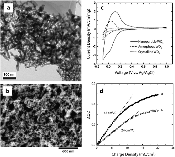 | ||
| Fig. 3 WO3 nanocrystals for electrochromic devices. (a) TEM micrograph of WO3 nanocrystals synthesized by HWCVD. (b) SEM micrograph of WO3 nanocrystal electrochromic electrode. (c) Cyclic voltammograms (scan rate: 20 mV s−1) displaying the enhanced charge capacity of nanocrystalline WO3. (d) Change in optical density at 670 nm upon charging a mixture of nanorods and nanospheroids (open circles) and nanospheroids only (closed circles). Reprinted with permission from ref. 22. Copyright © 2006 WILEY-VCH Verlag GmbH & Co. KGaA, Weinheim. | ||
Interesting results have also been reported for nanostructured NiO. In 2005, Deb and coworkers reported pseudocapacitive electrochromism in electrodes of NiO nanoparticles embedded in a Ta2O5 proton-conducting matrix (Fig. 4).23 By maximizing the surface area of the NiO within the matrix, the authors maximized the specific capacitance of the electrodes and the degree of optical modulation while achieving a colouration efficiency comparable to conventional NiO thin films. This important result demonstrated the feasibility of capacitive electrochromic mechanisms that avoid ion intercalation. Presumably, pseudocapacitive mechanisms in nanoparticle electrochromic electrodes should therefore confer enhanced durability and switching speeds, though the authors did not report these characteristics of their NiO particle films.
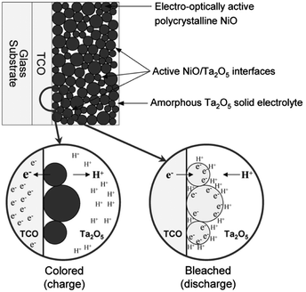 | ||
| Fig. 4 Nanostructured NiO electrochromic device. NiO nanoparticles are dispersed in an amorphous Ta2O5 matrix, which also acts as an electrolyte for protons. When electrons are injected, protons in the electrolyte adsorb onto the particle surfaces and the nickel ions are reduced at the surface through a pseudocapacitive process. As a result, the electrode bleaches according to the anodic colouration mechanism of NiO. Reprinted with permission from ref. 23. Copyright 2005 The Electrochemical Society. | ||
In addition to these “bottom up” approaches utilizing nanoparticles, there are also some exciting accounts of using patterning and templating approaches to generate electrochromic nanostructures. In particular, the Steiner group at Cambridge has used block copolymers to template NiO and V2O5 into gyroidal and mesoporous three-dimensional networks via electrodeposition.24,28 These periodic structures exhibit remarkably high surface areas, allowing for exceptional electrochemical and electrochromic performance. The V2O5 structure, operated as a pseudocapacitor, obtained a relatively high specific capacitance of 155 F g−1 along with a fairly strong green-to-yellow colour change. Remarkably, the gyroidal NiO structure not only had a switching time nearly two orders of magnitude faster than in thin films, but also displayed significantly higher optical contrast and comparable colouration efficiency (Fig. 5). Templating approaches are particularly interesting because they can potentially be applied to enhance the performance of many different electrochromic materials, either by reducing ion diffusion lengths within the material or by increasing the electrode–electrolyte interfacial surface area.
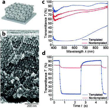 | ||
| Fig. 5 Block copolymer-templated gyroidal NiO electrochromic electrodes. (a) Schematic of mesoporous electrode. (b) SEM micrograph of gyroidal NiO. (c) UV-visible spectroscopy shows that templated NiO shows a significantly enhanced electrochromic response compared to non-templated NiO. (d) Time-resolved spectroscopy at 630 nm shows a much faster and deeper response for mesoporous NiO, with colouration and bleaching times of 63 and 53 ms, respectively. Reprinted with permission from ref. 24. Copyright 2013 American Chemical Society. | ||
The above nanomaterials approaches for electrochromic devices represent promising progress towards creating smart windows that are durable, efficient, and inexpensive. These methods may allow researchers to maximize the performance of devices based on conventional materials; however, it is unclear if truly new functionality can be arrived at by nanostructuring alone. Redox reactions underlying device operation are still frequently accompanied by ion insertion, so durability can remain a challenge even as nanostructuring can moderate the impact of such processes on material degradation. Furthermore, as long as the material compositions are drawn from the traditional selection of transition metal oxides, their optical characteristics remain subject to the limitations introduced in Section 1: they do not offer independent control over visible and NIR light, which limits their overall utility.
5. The emergence of electrochromism in colloidal nanocrystals of non-conventional materials
While nanostructured materials provide some promising improvements in electrochromic performance, nanostructuring alone does not appear to be sufficient to produce an ideal smart window with the characteristics proposed in Table 1. Despite their benefits, nanomaterials of conventional electrochromes still fall short of creating new functionality. Nonetheless, one of the most promising characteristics of electrochromic nanomaterials is the exploitation of a new operating mechanism: pseudocapacitance. New, NIR-selective functionality, sought after for an ideal smart window, might therefore be enabled by combining a new operating mechanism that is enabled by using nanomaterials (capacitance) with new materials that exhibit a different type of light absorption process. Such an absorption process would ideally be tunable across the solar spectrum and not broad-band. In the following sections, we will see that colloidal metal and doped metal oxide nanocrystals fit this description. Due to their extremely small size and high surface area, they can easily be electrochemically charged in a capacitive manner. Furthermore, these nanocrystals absorb or reflect light through localized surface plasmon resonance, which is relatively spectrally narrow and can be tuned across the entire solar spectrum by changing the material or by doping. We will also see that electrochemical injection or extraction of electrons can dynamically change the intensity and spectral position of LSPR absorption. This discovery gives rise to a new type of electrochromic device that has NIR-selectivity and excellent durability, bringing us closer to the ideal smart window. Plasmonic features and tunable absorption in the materials we discuss in the next two sections are specifically enabled by nanostructuring, and our approach has been to employ colloidal nanocrystals to tune size and composition to rapidly advance the development of plasmonic electrochromism.The field of colloidal nanocrystals and quantum dots is vast, and encompasses nearly all types of inorganic materials. Since the demonstration of quantum confinement in CdS quantum dots by Brus,29 an enormous amount of research has focused on synthesizing colloidal nanocrystals of new materials and observing new nanoscale phenomena. Optical phenomena, in particular, have captured the attention of physicists, chemists, and engineers alike, as nanocrystals tend to exhibit unique absorption, emission, and scattering behavior. In this section, and throughout the rest of this review, we will focus on manipulating light absorption and scattering by free carriers in nanocrystals. Electrochromism results when such manipulation can be carried out electrochemically. We will see that most strategies in this vein rely on the dynamically changing LSPR in nanocrystals.
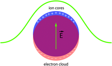
Localized surface plasmons are collective oscillations of conduction band electrons (or holes in the valence band) in response to incident electromagnetic radiation (Fig. 6).30 When the frequency of the radiation is close to the resonance condition of the free carriers, the nanocrystal exhibits significantly enhanced light absorption and scattering. Substantial effort has been expended to understand and control the optical properties of LSPRs in nanocrystals since Faraday's descriptions of gold colloids and Mie's theoretical treatments of their optical spectra.31 The literature now abounds with examples of manipulating LSPRs in nanostructures, either by synthetic control (changing nanocrystal size or shape,32 alloying,33,34 doping35) or by post-synthetic treatments (chemical,36,37 photochemical,38,39 or electrochemical manipulation40–43). A thorough treatment of these manipulations is far beyond the scope of this review (for discussions on plasmon resonance in nanocrystals and nanostructures, see ref. 30, 31, 44–53), but we will introduce the important experiments leading up to the birth of capacitive plasmonic electrochromics.
The relationship between free carrier concentration in a nanocrystal and the LSPR frequency is given by the following expressions:31,36
 | (4) |
 | (5) |
Henglein, Mulvaney, and Linnert provided one of the first examples of chemically induced changes to LSPR in colloidal Ag suspensions in 1991.55 The authors subjected aqueous suspensions of Ag oligomeric clusters or nanoparticles to ionizing radiation, which generated radicals that would diffuse to particle surfaces and either reduce the Ag colloids by injecting electrons, or extract electrons to oxidize the colloids. Electron injection was confirmed by measuring the associated increase in the DC conductivity of the suspension. Concurrently, the LSPR absorption peak blue shifted, narrowed in width, and grew more intense, confirming the increase in electron concentration in the Ag colloids (Fig. 7a). Upon oxidation, the decrease in electron concentration caused the LSPR peak to red shift, broaden, and decrease in intensity. While the optical changes were chemically induced and not electrochromic in nature, this important experiment laid the foundation for plasmonic electrochromism by showing that injection or extraction of electrons in colloidal metal nanoparticles results in a shift in the LSPR wavelength. In doing so, the authors set the stage for the following two decades of research on manipulating LSPR features through chemical, photochemical, and electrochemical doping.
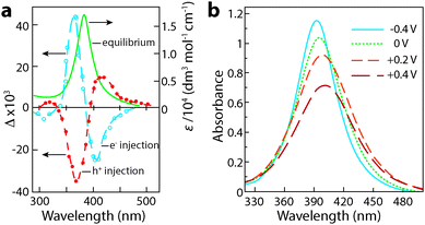 | ||
| Fig. 7 Chemical and electrochemical manipulation of LSPR in colloidal Ag nanocrystals. (a) Chemical manipulation of electron concentration using hydroxide radicals. The solid curve is the original plasmon absorbance, while the open circles represent the change in absorbance upon reduction, and the closed circles represent the change in absorbance upon oxidation. Adapted from ref. 55, copyright 1991, with permission from the Royal Society of Chemistry. (b) Absorbance of Ag nanocrystals at various potentials vs. Ag/AgCl. Adapted with permission from ref. 41. Copyright 1997 American Chemical Society. | ||
Mulvaney et al. built upon this work in 1997 by electrochemically doping colloidal silver.41 Using an aqueous electrolyte solution containing polymer-stabilized Ag nanoparticles, the authors employed in situ spectroelectrochemistry to cathodically charge the silver colloids. As individual particles diffused towards the negative working electrode, electrons tunneled into the particles and were compensated by ionic charge in the electrolyte through formation of a double layer. As charging occurred, the plasmon absorption peak simultaneously blue shifted, increased in intensity, and narrowed (Fig. 7b). It was possible to reverse the process, and even to anodically “bleach” the particles by removing electrons, causing a red shift, broadening, and decreasing intensity of the plasmon absorption peak. Over the entire stable voltage window, 1790 electrons were transferred into or out of each 9.8 nm diameter silver nanoparticle to modulate the plasmon resonance wavelength between 404 nm and 392 nm. While the shift in the absorption peak was small (owing to the high intrinsic carrier density of silver), this experiment demonstrated an entirely new type of electrochromism based on electrochemical manipulation of plasmon absorption in nanoparticles.
Wang, Shim, and Guyot-Sionnest broadened the field into chalcogenide nanocrystals with their demonstration of electrochromism in colloidal dispersions of CdSe quantum dots in 2001.56 Fourier transform infrared (FTIR) and UV-visible spectroscopies were used to measure the absorption and photoluminescence (PL) of the charged nanocrystals by monitoring the reflectivity of the optically polished Pt working electrode. Upon electron transfer into the CdSe, the dispersion exhibited a new mid-IR absorption peak, along with bleaching in the visible and quenching of the PL (Fig. 8). These optical effects are due to injected electrons occupying the 1S state in the nanocrystals; the new IR absorption is indicative of intraband transitions from 1S to 1P, while the visible bleach is due to filling of the 1S states, which prevents the lowest energy interband transitions as well as PL. Both electron injection and the optical changes were fully reversible, although the authors were not able to inject stable holes or observe any related optical effects. It was also shown that the energy and intensity of these transitions could be manipulated by changing nanocrystal size, owing to the quantum confinement effect in CdSe quantum dots. Guyot-Sionnest et al. subsequently built upon these results by processing 4.2–6.8 nm CdSe nanocrystals into thin films.57,58 Those films, when properly prepared, exhibited fast, intense electrochromism on a time scale of about 100 ms, and were durable enough to last for over 10![[thin space (1/6-em)]](https://www.rsc.org/images/entities/char_2009.gif) 000 cycles.
000 cycles.
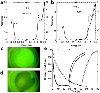 | ||
| Fig. 8 Electrochromism of CdSe quantum dots. (a) Optical response of a colloidal dispersion of 5.4 nm CdSe nanocrystals upon applying a negative potential. (b) Electrochromic response of a colloidal suspension 7.0 nm CdSe nanocrystals. (c) Photograph of uncharged CdSe suspension under UV illumination, displaying photoluminescence. (d) The PL is quenched upon charging the CdSe quantum dots. (e) Time response of the bleaching at 1.94 eV for 6.2 nm diameter CdSe nanocrystal films with different surface treatments. The solid lines are the response with voltage set to zero after the negative potential step; the dotted lines are the response of the film disconnected from the potentiostat after the negative potential step. Parts (a) through (d) from ref. 56. Reprinted with permission from AAAS. Part (e) reprinted with permission from ref. 58. Copyright 2003 American Chemical Society. | ||
These types of spectroelectrochemical experiments were extended to highly doped and conductive metal oxide nanocrystals between 1999 and 2002. Boschloo and Fitzmaurice were the first to prepare thin films of nanocrystalline antimony-doped tin dioxide (Sb:SnO2 or ATO) on conductive substrates and electrochemically charge them to achieve an electrochromic effect.59 By performing Mott–Schottky analysis, they measured the pH-dependent flat-band potential of ATO, followed by spectroelectrochemistry. At potentials greater than the flat-band potential, a depletion layer formed within the nanocrystals at the interface with the electrolyte concurrent with an observed decrease in absorption, while at potentials less than the flat-band potential, the absorption increased as electrons were injected into the ATO. The spectral changes were fully reversible, and the charge was injected capacitively, rather than through Faradaic, ion-insertion, or other redox reactions. The authors ascribe the increased absorption at short wavelengths to optical band gap widening through the Burstein–Moss effect, and at longer wavelengths to electron “Drude absorption,” but their spectral results do not extend to sufficiently long wavelengths to observe a shifting NIR absorption peak that would be characteristic of plasmonic electrochromism.
In 2000, recognizing the potential to use capacitive charge injection in nanocrystals for electrochromic devices, zum Felde, Haase, and Weller worked to maximize the electrochromic effect in films of ATO nanocrystals.25 By synthesizing their own nanocrystals to achieve small sizes with controlled Sb content and electrode layer porosity, the authors were able to drastically increase the changes in optical density with voltage, on a time scale of about 150 ms, and with a colouration efficiency of 18 cm2 C−1 (at λ = 650 nm). In this case, a NIR absorption peak centered at wavelengths between 2000 nm and 3000 nm was indeed observed in the prepared films, and ascribed to LSPR in part because the peak wavelength depended on the extent of Sb doping. The magnitude of this absorption feature increased as electrons were injected into the nanocrystalline network, yet the frequency of the plasmon peak did not change, suggesting that the concentration of free electrons remained constant (Fig. 9). To rationalize this observation, the authors proposed that a depletion region exists near the surface of the nanocrystals, arising from factors such as reduction of Sb5+ to Sb3+ at the surfaces and other surface electron trap states. In such a scenario, the depletion layer shrinks as electrons are injected into the nanocrystal, maintaining a constant electron concentration even as the overall population of electrons changes substantially. Strongly negative potentials induced increased absorption in the visible as well as the NIR, which the authors ascribed to electrochemical reduction of Sb5+ to Sb3+ accompanied by cation insertion. Pflughoefft and Weller followed up on this observation in 2002, attributing the visible absorption to Sb3+Cl−Sb5+ and Sb3+O2−Sb5+ charge-transfer complexes.60
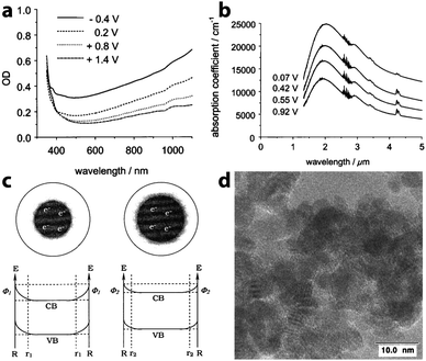 | ||
| Fig. 9 Electrochromic response of Sb-doped tin oxide nanocrystal films. (a) Visible absorption at different potentials vs. Ag/AgCl. (b) NIR absorption response at different potentials vs. Ag/AgCl. (c) Illustration of the effects of a depletion layer on the electron concentration. As the potential is decreased (from left to right), electrons are injected, but the width of the depletion region also decreases, resulting in no change in the carrier concentration. (d) TEM micrograph of ATO nanocrystals. Reprinted with permission from ref. 25. Copyright 2000 American Chemical Society. | ||
6. A new paradigm: NIR-selective dynamic plasmonic electrochromism in doped metal oxide nanocrystals
The experiments described above were foundational in elucidating a new type of electrochromism based on electrochemical injection or extraction of electrons into or out of plasmonic nanocrystals via capacitive charging. In such nanocrystals, a change in electron concentration should result in a shift in the LSPR absorption frequency and a change in absorption intensity, giving rise to plasmonic electrochromism.These early experimental results, however, fell short of challenging conventional electrochromics for applications such as smart windows:
• Although metal nanoparticles exhibit very strong LSPR absorption and Ag colloids were the first plasmonic electrochromic system, the high carrier concentration (∼1023 cm−3) severely limits the spectral range over which the plasmon resonance can be tuned. In an electrochemical capacitor-like geometry, the maximum number of electrons that can be injected into each nanocrystal is limited by factors such as the voltage stability window of the electrolyte and the electrode, the size/surface area of individual nanocrystals, and the polarizability of the nanocrystals and electrolyte. If the electron concentration is already quite high, then this maximum number of injected electrons will have a smaller effect on the plasmon absorption. Metals also screen the electric fields from the electrolyte more strongly than other materials, further limiting the extent to which the electron population can be modulated.
• While ATO nanocrystals showed much stronger electrochromism than metal nanocrystals, the majority of the electrochromic effect occurred at longer wavelengths in the NIR and mid-IR where there is not much solar isolation. Whether due to processing methods or inherent material limitations, an electrochemically-induced blue shift in the LSPR frequency to more relevant wavelengths has not been observed for ATO.
• Likewise, the optical changes of electrochromic CdSe are unsuitable for smart windows. Visible contrast is not sufficiently high, and the IR response of CdSe is in the mid-IR, where it is not useful for blocking solar heat gain.
Transparent conducting oxides (TCOs) are a class of material that have the potential to avoid these shortcomings. Bulk tin-doped indium oxide (ITO) and aluminum-doped zinc oxide (AZO), in particular, have carrier concentrations intermediate between semiconductors and metals (∼1021 cm−3), placing their plasma frequencies in the NIR.61 Recent work has demonstrated that ITO and AZO can be synthesized as monodisperse and colloidally stable nanocrystals.54,62–64 Due to the high conductivity of ITO and AZO, both materials have been shown to support strong LSPRs in the NIR, ranging from wavelengths of about 1600 nm to 4000 nm.54,63,64 Thanks to the efforts of many researchers over the past five years, including those in our group, synthetic protocols for ITO and AZO nanocrystals are now robust, allowing for control of nanocrystal sizes, doping levels, and optical properties. As detailed in Section 7, the synthetic control achieved over these nanocrystals is a key recent development that has made our work on plasmonic electrochromism possible.
We first reported the exceptional electrochromic properties of ITO nanocrystals in 2011. After synthesizing colloidal ITO nanocrystals of various sizes and doping levels, Garcia et al. processed them into continuous, electrically connected microporous thin films.14 This was accomplished by spincoating the nanocrystals, with their native organic ligands attached, onto ITO-coated glass substrates. The films were then treated with a formic acid solution to displace the ligands by mass action. Formic acid molecules at the nanocrystal surfaces were easily removed by annealing in an inert atmosphere, providing electrical conductivity throughout the entire film while leaving the micropores between nanocrystals intact, which allowed for electrolyte penetration throughout the film.
Upon immersing the ITO nanocrystal film in a LiClO4 electrolyte and applying a negative bias in a spectroelectrochemical experiment, a large LSPR blue shift was observed, causing up to unity change in optical density at NIR wavelengths for 150 nm-thick films. Even greater modulation was observed for thicker films. The shift in LSPR absorption frequency indicated that the electron density was indeed changing with electrochemical potential, indicating that the ITO nanocrystals were operating in an electrochemically stable accumulation regime. The large shift also indicated that, unlike ATO nanocrystal films,25 the ITO nanocrystals were relatively free of surface defects and the associated depletion layer modulation.14 Applying a positive potential easily reversed the optical changes, and the plasmon could even be red shifted from its equilibrium position, causing a bleach in absorption and indicating a transition to a depletion regime. Drude modeling confirmed that the carrier concentration increased over threefold from about 4.5 × 1020 cm−3 at the most positive bias to over 1.4 × 1021 cm−3 at the most negative bias.
Ultimately, smaller, more highly doped nanocrystals gave the strongest modulation of solar transmittance by allowing accumulation and depletion layers to extend farther into their interior volume and increasing the blue shift of the LSPR peak into the range of the NIR with higher insolation. These nanocrystals modulated the integrated NIR solar transmittance by 35% with only a 6% change in integrated visible transmittance. The wavelength-dependent colouration efficiency ranged from 25 cm2 C−1 at 1200 nm to nearly 200 cm2 C−1 at 1700–1800 nm. The electrochromic response was the same in Li+-containing electrolytes that support possible insertion reactions as in tetrabutylammonium ion-containing electrolytes where insertion was sterically prohibitive, indicating that capacitive charging is the dominant electrochromic mechanism. This mechanism enabled fast colouration and bleaching processes, and one should expect that capacitive operation should also promote long cycle life. The capacitive nature of the electrochromic effect, and the associated optical changes in the ITO nanocrystals, is depicted in Fig. 10.
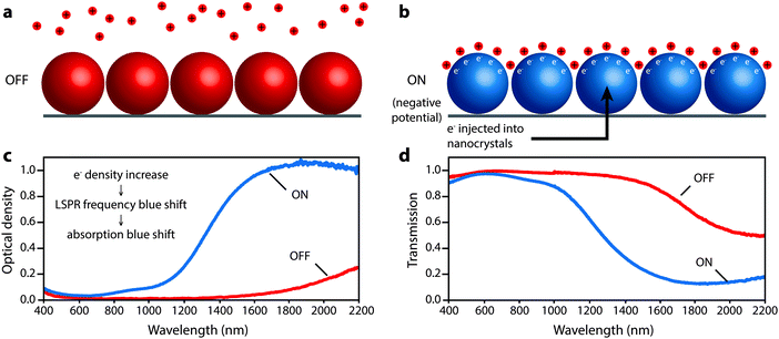 | ||
| Fig. 10 Depiction of the microscopic operation of a nanocrystal-based plasmonic electrochromic film, along with the associated optical changes. (a) In the OFF state, positive potential is applied to the nanocrystals, which are depleted of electrons and lithium ions are repelled. (b) In the ON state, a negative potential is applied to the nanocrystals, which injects electrons. Lithium ions are attracted to the nanocrystal surface to compensate the injected charge capacitively. (c) Optical density changes resulting from electron injection. The increase in carrier density causes a blue shift in the LSPR and absorption. (d) Corresponding changes in transmission of the film. Parts (c) and (d) adapted with permission from ref. 14. Copyright 2011 American Chemical Society. | ||
Garcia, et al. next examined the electrochromism of AZO nanocrystal films and compared them to ITO films,15 utilizing a newly-developed “Meerwein's salt” ligand stripping procedure to avoid dissolution or etching of the AZO nanocrystals in formic acid.65 The NIR modulation of AZO and particularly its durability bettered that of ITO, even though ITO's colouration efficiency had also been improved since the original report. This was ascribed to the enhanced electrochemical stability of Al3+ dopants in AZO relative to Sn4+ in ITO, which improved durability and allowed for more negative potentials to be applied to AZO, increasing the number of injected electrons without irreversibly reducing the metal ions. Overall, with changes in optical density of up to 2.5, the best AZO films achieved a 39% modulation in solar NIR transmittance, while the transmittance of visible sunlight changed by only 4%. This corresponded to colouration efficiencies of about 50 cm2 C−1 at 1100 nm and up to over 400 cm2 C−1 at 2000 nm. Colouration efficiencies in the ITO films ranged from about 50 cm2 C−1 at 1200 nm to a maximum of about 375 cm2 C−1 at 1700–1800 nm. These values are extremely high compared to conventional transition metal oxide electrochromic materials, which are typically in the range of 20–100 cm2 C−1.
This study also demonstrated the excellent switching speed and durability of nanocrystal-based electrochromics.15 The switching speeds for AZO were extremely fast, ranging between 0.06 and 0.9 seconds depending on the electrolyte composition, while for ITO the switching speeds were between 0.05 and 3.4 seconds. Both ITO and AZO nanocrystal films were subjected to 20![[thin space (1/6-em)]](https://www.rsc.org/images/entities/char_2009.gif) 000 electrochemical cycles, and their electrochromic and charge-storage properties were measured both before and after the cycling (Fig. 11). The AZO film lost only 11% of its charge capacity with little change in optical performance. On the other hand, the ITO film suffered a 45% reduction in charge capacity. The loss in capacity moderately reduced the optical modulation range of ITO, and was attributed to free carrier loss due to irreversible reduction of Sn4+ to Sn2+. These results demonstrate that TCO nanocrystal-based electrochromics, based on capacitive electrochemical injection and extraction of electrons, have the potential to be effective as NIR-selective smart windows with fast and deep colouration as well as good durability. AZO also has the added benefits of low cost and earth abundance compared to ITO.
000 electrochemical cycles, and their electrochromic and charge-storage properties were measured both before and after the cycling (Fig. 11). The AZO film lost only 11% of its charge capacity with little change in optical performance. On the other hand, the ITO film suffered a 45% reduction in charge capacity. The loss in capacity moderately reduced the optical modulation range of ITO, and was attributed to free carrier loss due to irreversible reduction of Sn4+ to Sn2+. These results demonstrate that TCO nanocrystal-based electrochromics, based on capacitive electrochemical injection and extraction of electrons, have the potential to be effective as NIR-selective smart windows with fast and deep colouration as well as good durability. AZO also has the added benefits of low cost and earth abundance compared to ITO.
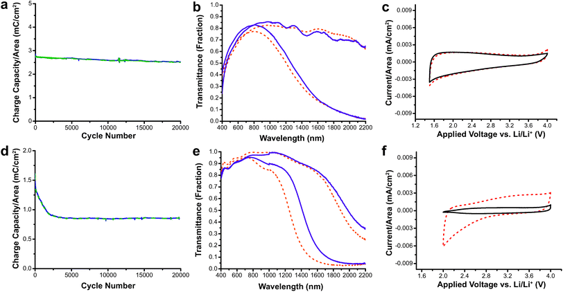 | ||
Fig. 11 Durability testing of AZO and ITO electrochromic nanocrystal films. (a) Charge capacity of AZO films vs. cycle number. (b) Transmittance modulation AZO nanocrystal film before (dashed lines) and after 20![[thin space (1/6-em)]](https://www.rsc.org/images/entities/char_2009.gif) 000 cycles (solid lines). (c) Cyclic voltammogram of AZO films before (dashed line) and after (solid line) cycling shows little change in electrochemical properties. (d) Charge capacity of ITO films vs. cycle number. (e) Optical modulation of ITO nanocrystal film before (dashed lines) and after (solid lines) 20 000 cycles (solid lines). (c) Cyclic voltammogram of AZO films before (dashed line) and after (solid line) cycling shows little change in electrochemical properties. (d) Charge capacity of ITO films vs. cycle number. (e) Optical modulation of ITO nanocrystal film before (dashed lines) and after (solid lines) 20![[thin space (1/6-em)]](https://www.rsc.org/images/entities/char_2009.gif) 000 cycles. (f) The cyclic voltammogram for ITO shows diminished charge capacity after 20 000 cycles. (f) The cyclic voltammogram for ITO shows diminished charge capacity after 20![[thin space (1/6-em)]](https://www.rsc.org/images/entities/char_2009.gif) 000 cycles (solid line). Reprinted with permission from ref. 15. Copyright © 2013 WILEY-VCH Verlag GmbH & Co. KGaA, Weinheim. 000 cycles (solid line). Reprinted with permission from ref. 15. Copyright © 2013 WILEY-VCH Verlag GmbH & Co. KGaA, Weinheim. | ||
7. Design principles for nanocrystal-based plasmonic electrochromics
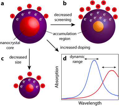
The realization of nanocrystal-based plasmonic electrochromics would have not been possible without the recent advancement of methods for synthesizing doped metal oxides and other doped semiconductor nanocrystal colloids. In this section, we present the design principles—doping, size, and material selection—for nanocrystal-based plasmonic electrochromics, and describe how colloidal nanocrystal synthesis can be leveraged to meet these design principles. In particular, we will present doping strategies that enable the generation of free electrons in colloidal metal oxide nanocrystals, and thus, LSPRs in the NIR. We will also address the experimental limitations of aliovalent substitutional doping and highlight the exploration of plasmonic nanocrystal materials beyond TCOs. Finally, we discuss the influence of nanocrystal size and dopant concentration on the LSPR modulation.Maximizing the shift in plasmon resonance and the associated modulation of NIR radiation is still a key challenge to improving the functionality and the energy saving capabilities of plasmonic smart windows. As observed in ITO and other semiconductor nanocrystals, higher doping shifts the equilibrium position of the LSPR peak to higher frequency, moving it closer to a region of appreciable solar energy. By comparison, the relationship between decreasing nanocrystal size and enhanced optical modulation remains mysterious. At smaller radii, nanocrystals have a larger surface to volume ratio, giving higher capacitance and allowing for more electrons to be injected. Smaller nanocrystals will also have a larger increase in electron concentration within the accumulation region for a given accumulation layer thickness. It is unclear which of these two effects is the limiting mechanism in determining the ultimate free electron concentration achievable by capacitive charging. However, as a general design principle for NIR-selective plasmonic electrochromics, small and highly doped plasmonic metal oxide nanocrystals should be used to maximize optical modulation in the NIR range of the solar spectrum. In addition, materials that weakly screen external electric fields (unlike metals, as discussed at the beginning of Section 6) allow the electron accumulation region to extend as far as possible into the nanocrystal core. This allows for the maximum number of electrons to be injected, corresponding to greater changes in the plasmon peak position. These design principles are summarized in Fig. 12. As this field progresses, we expect that the material that combines small nanocrystal size, high doping level, and low screening of electric fields will provide the best electrochromic performance.
To achieve changes in nanocrystal doping, size, or to utilize new plasmonic materials, our group has turned to organic phase colloidal nanocrystal synthesis. The well-established surfactant-mediated method for colloidal synthesis allows one to grow nanocrystals from molecular precursors in solution phase at moderate temperatures between 150 °C and 400 °C (Fig. 13). Surfactant-assisted colloidal synthesis offers excellent control over nanocrystal size and shape, as well as preventing their aggregation and precipitation from solution,66–69 which enables stable colloidal dispersions (Fig. 13c). Such dispersions can serve as inks for solution deposition of nanocrystal films using potentially low cost and industrially scalable techniques such as spray coating or slot die coating, as well as laboratory-scale techniques like spin coating. More recently, it has become possible to finely control nanocrystal composition, providing enhanced tunability of dopant concentrations and hence LSPR frequency.54,64,70 These advances have been critical for the development of LSPR-based nanocrystal electrochromics, and have also contributed momentum to new research on plasmonic optoelectronics.71,72
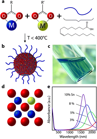 | ||
| Fig. 13 Colloidal synthesis of doped metal oxide nanocrystals. (a) Molecular precursors (depicted here as metal carboxylates) are combined with ligands (oleic acid depicted) in a non-polar solvent and heated to moderate temperatures. (b) After the precursors decompose and react, inorganic colloidal nanocrystals are formed, which are stabilized in solution by the ligands coordinated to the surface. (c) Optically clear dispersion of colloidal ITO nanocrystals in hexane. (d) Substitutional doping mechanism whereby a donor atom (i.e. Sn) occupies a metal (i.e. In) site in the nanocrystal, thereby introducing electrons into the conduction band. (e) Absorbance spectra of ITO nanocrystals, showing a blueshift, narrowing, and enhanced intensity of the plasmon peak as doping increases. Part (e) adapted with permission from ref. 54. Copyright 2009 American Chemical Society. | ||
A critical aspect that was not investigated in the seminal experiments on the electrochromism of ATO nanocrystals was the influence of nanocrystal size.25,59,60 Varying nanocrystal size, as was done for colloidal CdSe quantum dots,56,57 provides the opportunity to better understand the fundamental mechanisms at work in nanoscale electrochromic materials. In the case of ATO, however, the nanocrystals were synthesized by a coprecipitation method, which limited the opportunity to tune nanocrystal size over a broad range, obtain monodisperse size distributions, and achieve higher degrees of crystallinity. Now that organic phase colloidal methods have advanced for doped oxide nanocrystals, we can access stable colloidal dispersions (Fig. 13c) with monodisperse nanocrystal dimensions that can be tuned from 1 nm to 30 nm.
While the field of colloidal synthesis is well developed and small-diameter nanocrystals on the order of 1 nm can be obtained, achieving high doping levels has been more elusive and challenging.73–76 The emergence of plasmonic semiconductor nanocrystals has done much to motivate research on doping strategies. Today, chemists have achieved far better control over the incorporation of dopants into colloidal nanocrystals, and can now do so with a high degree of control over the dopant content35 (Fig. 13e).
Growing colloidal nanocrystals from solution phase is a kinetically controlled process; introducing dopants within the lattice (Fig. 13d) therefore requires a fine balance of the host nanocrystal growth rate and the dopant incorporation rate. A variety of doping strategies have been reported for several nanocrystal compositions, and they have been recently reviewed and discussed in depth.35 For the particular case of binary metal oxides, the most popular doping strategy is based on tuning the relative chemical reactivity of the molecular precursors for the host nanocrystal and for the dopant atom. Typical precursors are metal–organic salts comprising the metal of interest and a ligand (e.g. an alkyl carboxylate). By selecting a ligand with the appropriate steric hindrance and negative charge delocalization properties, it is possible to tune the ligand–metal bond strength to balance the reactivity of both precursors. By developing this strategy, our group was able to demonstrate the first synthesis of plasmonic, monodisperse Al-doped ZnO nanocrystals of controlled sizes and dopant levels.15,64 Substitutional doping strategies have been also proven successful for other TCO nanocrystals, such as Sn-doped In2O3,54,62 Nb-doped TiO2,77 and In-doped CdO.70
Understanding the role of size and doping on the electrochromic response of plasmonic nanocrystals is of tremendous importance to generate fundamental knowledge about the mechanism of plasmon modulation as well as generating design rules for these novel materials. The fine control over size and composition offered by colloidal synthesis has enabled our group to pioneer these systematic studies by synthesizing colloidal plasmonic nanocrystals (ITO and AZO) over broad size ranges (4 nm up to 16 nm) (Fig. 14), with narrow size distributions (<15% std. deviation in diameter), a high degree of crystallinity, and well-controlled dopant concentrations.14,64
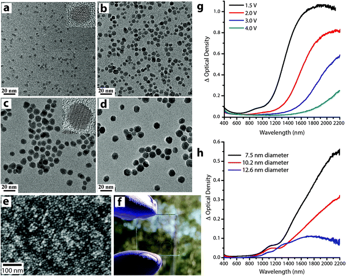 | ||
| Fig. 14 (a–d) Transmission electron microscopy images of ITO nanocrystals with sizes (nm): (a) 4.1 ± 0.6, (b) 7.4 ± 1.4, (c) 10.2 ± 1.7, and (d) 12.1 ± 1.5. (e) Scanning electron image (top view) and (f) photograph of an ITO NC network film on glass substrate. (g) Optical density at different applied voltages of an ITO nanocrystal network film with 4.1 nm diameter, 16.8% Sn nanocrystals. (h) Change in optical density between 1.5 V and 4 V (vs. Li/Li+) for various nanocrystal sizes, each with 4.65 ± 0.25% Sn. Parts (a–d), (g) and (h) reprinted with permission from ref. 14. Copyright 2011 American Chemical Society. | ||
As mentioned earlier, the electrochromic response of our ITO nanocrystal films induced a substantial spectral shift upon charge injection (Fig. 14g), indicating that the nanocrystals operate in an electrochemically stable accumulation regime. Taking into account the capacitive nature of the electrochemical plasmon modulation, small nanocrystals are expected to show greater optical modulation since the entire volume can lie within the strongly modulated accumulation/depletion region. We confirmed this hypothesis by comparing the optical response of ITO nanocrystals with different sizes and similar doping level. As expected, the change in optical density increases as the average nanocrystal diameter decreases (Fig. 14h), and films made with the smallest nanocrystals showed the strongest optical modulation. The concentration of free electrons in the as-synthesized nanocrystals, determined by the doping level, also plays a key role because it determines the starting position, width, and intensity of the LSPR absorption peak14,54,55,70 (eqn (4) and (5) and Fig. 13e).
Given that most of the NIR solar energy is located at wavelengths between 750 nm and 1250 nm, it would be optimal to use nanocrystals with LSPRs near that range. Unfortunately, ITO nanocrystals, which so far display the “bluest” plasmons of TCO nanocrystals, have a minimum LSPR wavelength of about 1600–1700 nm.14,15,54 This limitation is due to the interplay and competition between doping and defect compensation mechanisms. In metal oxides, aliovalent dopants can be compensated by ionic defects like lattice vacancies and interstitials to maintain charge neutrality. For the particular case of ITO, in which free electrons are introduced by aliovalent substitution of Sn4+ for In3+, theoretical and structural studies have verified that neutral  defect clusters act as compensating defects.78–80 At high doping concentrations, the concentration of these clusters becomes significant, and the defect cluster formation reaction begins to deplete ITO of free electrons. The concentration of free electrons therefore depends on the relative concentration of substitutional tin atoms,
  , oxygen vacancies,
  , and oxygen interstitial atoms [Oi′′]. The concentrations of oxygen vacancies and interstitials further depend on the ambient partial pressure or activity of oxygen. This complex relationship has a direct influence in determining the optimum doping level and imposes a maximum carrier concentration that is achievable by extrinsic doping.81 Indeed, as in the bulk, optimum doping levels have been observed for ITO nanocrystals, above which the LSPR peak begins to redshift with increasing doping level.54 Development of new plasmonic colloidal metal oxide nanocrystals, with wavelengths closer to the 750 nm to 1250 nm range, will depend on selecting materials that overcome the limitations of defect compensation mechanisms and/or exploit new doping mechanisms, such as interstitial doping.53 Vacancy- and cesium-doped tungsten oxide are two examples of recently-developed plasmonic metal oxide nanocrystals with LSPR features within this region of interest.82,83
8. Using plasmonic nanocrystals as building blocks for advanced electrochromic devices
Similar to the key contributions of colloidal synthesis in the development of plasmonic electrochromic devices, surface chemistry is being leveraged to integrate plasmonic TCO nanocrystals into mesostructured electrodes with greater functionalities.16,17,84 The surfaces of the nanocrystals, when stripped of organic ligands, offer a unique chemical platform to rationally attach other components through interfacial bonding (Fig. 15a–c and f). These components can either add new functionalities to the electrochromic device16 or can be used as architecturing agents to form ordered mesoporous nanocrystal assemblies.85 For the past 4 years, our group and many other researchers have devoted great scientific effort to exploit and manipulate the surface chemistry of colloidal nanocrystals by employing ligand-exchange or ligand-stripping procedures to expose and/or modify bare nanocrystal surfaces.65,86,87 These experimental advancements have led to unprecedented dual-band “nanocrystal-in-glass” composites16,88 and mesoporous plasmonic nanocrystal assemblies with ordered, tunable pore sizes and enhanced charge capacity and switching kinetics.17 In addition, we recently showed that these electrodes can be successfully integrated into solid-state devices, providing the first demonstration of NIR-selective solid state electrochromic device.17 This exciting progress is paving the way for a new generation of advanced electrochromic devices.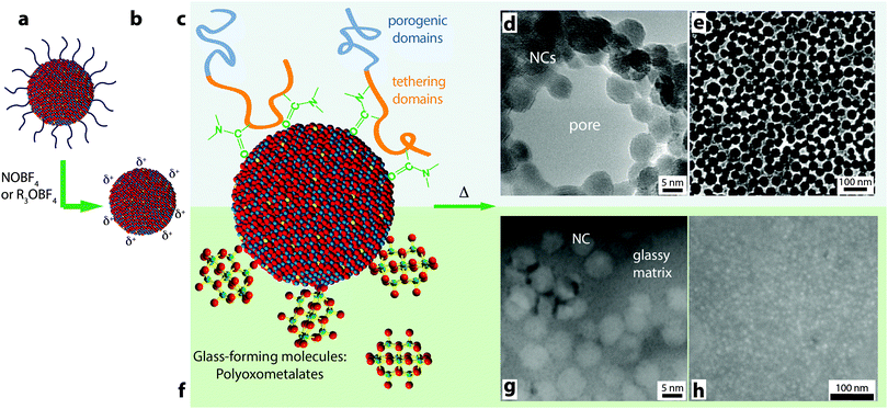 | ||
| Fig. 15 Schematic for using colloidal nanocrystals as building blocks for advanced electrochromic materials and devices. (a) Starting with the as-synthesized nanocrystals a ligand-stripping agent is used to produce (b) nanocrystals with bare, positively charged surfaces. (c) The nanocrystal surfaces can be decorated with amphiphilic block copolymers and made to form (d) micelles decorated with nanocrystals (TEM micrograph of a micelle). (e) Upon depositing the micelles and burning off the polymer, a mesoporous structure is obtained (SEM micrograph of film, top view). (f) Nanocrystal surfaces functionalized with POM clusters. Upon deposition and annealing, the POMs decompose to form a glassy matrix surrounding the nanocrystals. (g) TEM cross-section micrograph of a composite film. (h) SEM top-view micrograph of a composite film. Parts (d) and (e) reprinted with permission from ref. 85. Copyright 2012 American Chemical Society. Parts (g) and (h) reprinted with permission from ref. 16. Copyright 2013 Nature Publishing Group. | ||
As presented in Section 6, the simplest nanostructured plasmonic electrochromic electrode is constructed from randomly packed nanocrystals, forming an interconnected open network that yields 34% porosity.14,17 Given the capacitive operating mechanism, these electrodes must have high surface areas that are easily accessed by the electrolyte. An ITO nanocrystal electrode with 34% porosity functions well enough in liquid electrolyte to achieve dynamic changes of 40% in NIR transmittance.15 Nevertheless, the accessible surface area of active material is still limited in these films owing to insufficient nanocrystal–electrolyte interfacial contact or interpenetration, inefficient electron conduction within the nanocrystal network, or restricted electrolyte or ion motion within micropores between nanocrystals.15,17 All of these effects are detrimental to the dynamic modulation range, colouration efficiency, and switching kinetics of the electrode, and are dependent on the arrangement of ion- and electron-conducting domains in the nanocrystal electrode, the relative length scales of those domains, and the topology of their interfaces. We investigated the influence of pore size by utilizing amphiphilic block copolymer micelles to template ligand-stripped ITO nanocrystals into ordered and conductive mesoporous frameworks. By changing the molecular weights of the hydrophobic or hydrophilic block, the mesoporous architecture was easily controlled, with pores ranging from 29 nm to 37 nm and pore wall thicknesses ranging from 9 nm to 13 nm (Fig. 15e).17 Such exceptional mesoscale control and order was enabled through tailored, strong enthalpic interactions between the hydrophilic block and the ligand-stripped nanocrystal surfaces.85 Mesoporous ITO architectures showed comparable optical modulation, higher colouration efficiency, higher charge capacity, and enhanced charging kinetics when compared to randomly packed, microporous nanocrystal networks. The enhancement in switching speed scaled with increasing pore size, indicating that larger pores provided for faster ion transport to the nanocrystal surfaces.17
Perhaps even more important than improved colouration efficiency, charge capacity, and switching speed, mesostructured nanocrystal electrodes can be combined with polymer gel electrolytes to fabricate full-cell, solid-state electrochromic devices. We created full-cell devices by using a mesostructured ITO nanocrystal electrochromic electrode, a CeO2 nanocrystal counter electrode (which was optically passive), and a plasticized, poly(vinyl butyral) (PVB) gel electrolyte containing a lithium salt.17 Our PVB electrolyte was easily deposited on each electrode, penetrated into the mesopores of the ITO electrochromic electrode, and allowed the electrodes to be laminated together to produce a robust, solid-state device. The ionic conductivity of the electrolyte was ∼10−7 S cm−1, which was within acceptable limits for typical electrochromic devices8 and provided good switching speed (<10 s) for our devices.
When compared to an unarchitectured solid-state device using the same PVB-based electrolyte, mesoporous ITO nanocrystal films displayed greater than two-fold enhancements in optical modulation, colouration efficiency, and charge capacity.17 The 60% porosity of the mesoporous film, compared to the 34% porosity in the unarchitectured film, provided the solid electrolyte with improved access to and intimate contact with the nanocrystal surfaces. This is a key advance, as the continued development of nanocrystal-based electrochromics will likely depend on the ability to integrate nanocrystals into solid-state devices and manufacturing methods. The capability to produce mesostructured nanocrystal electrodes is therefore incredibly important for the continued development of these devices, as is improved understanding of the interactions between polymer electrolytes, lithium ions within such electrolytes, and nanocrystal surfaces.
Precise control over nanocrystal surface chemistry and assembly also provides an opportunity to combine plasmonic TCO nanocrystals with conventional transition metal oxide electrochromic materials. Such a device could approach the ideal functionality for a smart window, as the nanocrystals and conventional materials could be activated independently to modulate both the visible and NIR regions of the solar spectrum.89 “Dual-band” functionality would allow the window to operate in either hot or cold climates and respond to changing weather conditions, ultimately pushing past the current performance limits of either conventional or plasmonic nanocrystal electrochromics.90 In 2013, we demonstrated that this scientific challenge could be met by creating a composite material consisting of NIR-selective ITO nanocrystals dispersed in a matrix of a visibly colouring electrochromic material, amorphous niobium oxide (NbOx).16 To create the composite, anionic niobate polyoxometalate (POM) clusters were chemically linked to the surfaces of ligand-stripped colloidal ITO nanocrystals and thermally condensed, yielding a glassy metal oxide network that is covalently bonded to the nanocrystal surfaces (Fig. 15). Given that the reduction potential of NbOx is lower than the potential range for capacitive charging of ITO nanocrystals, the two optical responses can be independently controlled by simply modifying the applied voltage. Thus, for the first time, independent control of NIR and visible light in an electrochromic device has been demonstrated. Interestingly, we also found that structural reconstruction and interfacial doping between the nanocrystals and the glassy matrix strongly affected the optical contrast of the matrix, which was maximized at around 43 vol% ITO, reaching a value five times greater than that of pure NbOx when normalized by NbOx volume fraction (Fig. 16). Furthermore, the composite electrodes exhibited excellent initial durability, losing only 4% of their charge capacity over 2000 cycles.16 This, in comparison to the pure NbOx films (20% capacity loss) and pure ITO nanocrystal films (85% capacity loss) also examined in the study, indicates that the interactions and reconstructions in ITO-NbOx are key not only to enabling dual-band electrochromic operation, but also enhancing durability, opening the avenue to more robust and more efficient smart windows.
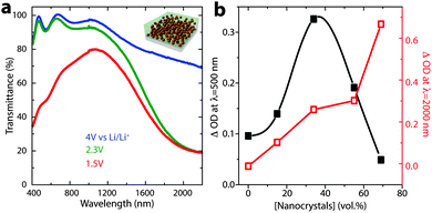 | ||
| Fig. 16 Dual-band electrochromic operation of ITO-NbOx nanocomposites. (a) Changing the applied potential between 4 V and 2.3 V vs. lithium induces NIR absorption, as electrons are injected into the ITO nanocrystals, changing their LSPR absorption. At potentials below the Li+ insertion potential (1.5 V), ions are inserted into and reduce the NbOx matrix, causing a visible colour change. (b) Optical contrast of the NbOx matrix (at 500 nm), and ITO nanocrystals (at 2000 nm), vs. ITO volume fraction. Interestingly, the NbOx contrast is maximized at intermediate nanocrystal concentrations, indicating synergistic interfacial enhancement. Figure adapted with permission from ref. 16. Copyright 2013 Nature Publishing Group. | ||
9. Conclusion and outlook
Electrochromism has captured the attention of academic and industrial researchers for the past several decades. Unfortunately, sustained and dramatic progress has been elusive, and the promise of electrochromic devices for smart windows, not to mention displays and other applications, has yet to be fully realized. With the advent of nanotechnology, however, it appears electrochromic devices may finally have the impetus needed to live up to their potential. Nanomaterials provide electrochromic devices with enhanced charge capacity, better colouration efficiency, and improved durability, even for conventional electrochromic materials. Furthermore, nanotechnology has provided the field with the discovery of a new class of electrochromism based on plasmonic colloidal nanocrystals, opening the door for new device functionalities, such as NIR selective optical modulation. Significantly, nanomaterials also present an opportunity for industry to move from energy- and cost-intensive vacuum deposition to solution processing methods, potentially drastically reducing the prices of smart windows.Colloidal TCO nanocrystals, as described in this review, appear to have significant potential to kick-start the progress of smart window technologies. Dynamic plasmonic electrochromism in these materials provides NIR-selective operation with exceptional colouration efficiency, switching time, and durability. Nonetheless, the range of NIR optical modulation in electrochromic TCO nanocrystals is not yet sufficient for smart window applications. Discovery of new TCO nanocrystals, with LSPR absorption peak wavelengths closer to 1250 nm, will be crucial for further development of plasmonic electrochromism. Recent literature is promising in this regard: newly-synthesized cesium-doped tungsten oxide nanocrystals display LSPR peaks at wavelengths as low as 900 nm,83 as do vacancy-doped WO2.83 nanorods.82 It remains to be seen if all plasmonic metal oxide nanocrystals are equally amenable to capacitive electrochemical charge injection—if indeed they are, then colloidal CsxWO3 and WO3−x nanocrystals are promising candidates for plasmonic electrochromic devices.
Optimizing and fully understanding dual-band control over visible and NIR light will play a key role in achieving ideal electrochromic device performance and future adoption of smart windows. This will require researchers to explore the feasibility of alternative nanocrystal-in-glass composites, thoroughly characterize the electrochemical cycling durability of these composites, and determine how processing conditions influence durability. There is ample opportunity to explore new material combinations of nanocrystals and POMs; thus far, dual-band functionality has been reported only for ITO-in-NbOx nanocomposites.16 For optimal performance, new material combinations should be explored, such as those using plasmonic nanocrystals with “bluer” LSPR features and glassy matrices with high colouration efficiencies and better selectivity for visible light. The versatility of the colloidal building block approach enables such exploration as it allows researchers to easily combine new nanocrystal and POM materials as they are being developed.88 One outstanding question is whether different nanocrystal-POM combinations will exhibit the same type of interfacial doping or synergy as ITO-in-NbOx, and whether enhanced electrochromic properties will result. The key for effective dual-band operation will be to discover material combinations for which the electrochemical potentials for capacitive charge injection (changing LSPR frequency) and ion insertion (changing visible absorption via polarons, etc.) are different enough to have three distinct operating regimes (transparent, selectively NIR-blocking, and NIR- and visible-blocking). Our group is currently working to discover new nanocrystal-POM combinations, to examine the bonding synergy between nanocrystals and POMs, and to evaluate electrochromism of new compositions of doped oxides like CsxWO3,83 WO3−x,82 and Nb-doped TiO2,77 both alone and within nanocrystal-in-glass composites.
As plasmonic electrochromic technology matures, full device integration will become an important gateway to commercialization. One particularly important aspect of device integration is the electrolyte, which, in a commercial device, usually needs to be solid state. We have begun to investigate this aspect, and have demonstrated the feasibility of solid-state nanocrystal electrochromic devices using gelled PVB electrolytes.17 This advance was not trivial, as successful device integration required advanced templating methods to generate mesostructured nanocrystal electrodes. It will be necessary to continue developing or modifying solid electrolyte formulations that interface well with nanocrystal electrodes and are amenable to large-scale processing. Solid or gelled polymer electrolytes appear to be promising candidates, and such electrolytes are often utilized in electrochromic devices. This is a significant challenge; polymer electrolytes are often the most closely guarded secrets of commercial smart window manufacturers, and continued research on polymer–nanocrystal interaction and co-processing of polymer electrolytes and plasmonic TCO nanocrystals is needed for this field to advance.
Other device integration challenges include development of counter-electrode materials and charge balancing. The ideal counter-electrode material for plasmonic electrochromic devices would be p-type TCO nanocrystals, which would theoretically display anodic colouration in the NIR upon capacitive charging. Unfortunately, due to limitations in oxide band structure and defect chemistry, p-type TCOs are not readily achievable in bulk form, much less in nanocrystal form. Nevertheless, some p-type plasmonic nanocrystals, such as Cu2−xS36 and Cu2−xSe,37 do exist, and other transparent p-type materials, such as Cu-doped ZnS,91 have recently been synthesized as thin films. If these materials can be adapted for use in plasmonic nanocrystal devices, they would likely greatly enhance the optical contrast and overall colouration efficiency. In the meantime, colloidal nanocrystals of cerium oxide (CeO2), a material which displays little colouration upon electrochemical charging and discharging,92 have been demonstrated as a useful, optically passive counter electrode in full devices.17 In any case, it is important to achieve charge balance between the counter electrode and the active electrode for optimum device performance.5,7,9 Charge balance will require careful evaluation of the charge capacities of the active and counter electrodes, in addition to the polarization and charge transport behaviour of the electrolyte.
One final challenge that bears mention is the continuing advancement of nanocrystal synthesis. For one, the advancement of nanocrystal-based electrochromic devices depends on further understanding and manipulation of colloidal chemistry, such that new materials can be synthesized with desired size, shape, and composition. In addition to these laboratory-scale advances, it will also be critical for chemical engineers to understand how to scale nanocrystal synthesis. Current lab-scale synthetic methods typically produce about 1–10 mmol of nanocrystals, which corresponds to 278 mg to 2.78 g of ITO nanocrystals. Industrial-level production of smart windows will eventually require ton-scale nanocrystal production. Scaling nanocrystal synthesis is not trivial, as the increased thermal mass of the colloidal dispersion can dramatically affect nanocrystal growth, and certain synthetic methods, such as precursor injection, are not amenable to large-scale synthesis. Large-scale synthesis has been demonstrated for a few types of nanocrystals, notably iron oxide,93 but it remains to be seen if the nanocrystals of specific interest for smart windows can be made with sufficient control over size and doping at scale.
As a parting note, we point out that more fundamental research is warranted for this new type of electrochromism. A number of open questions remain regarding understanding the fundamental limits of capacitive charging in TCO nanocrystals. Considering that injected carriers are stabilized by polarization of the surrounding electrolyte, how do the characteristics of the electrolyte contribute to the maximum achievable charging levels? For low potentials and small nanocrystals, it should be possible for the accumulation layer to become as large or larger than the nanocrystal volume. Does this limit the maximum colouration contrast achievable, or will smaller nanocrystals always increase the colouration contrast? We have also seen that polarizable materials, like TCOs, exhibit a broader electrochromic dynamic range than metals. Does this mean that the dielectric constants of the electrolyte and the nanocrystal drastically affect the number of electrons that can be injected? Or is the plasmon shift greater in ITO simply because its starting electron concentration is lower? How important are doping levels and the starting position of the plasmon absorption peak, and will materials like CsxWO3 indeed exhibit greater excursions through the NIR towards the visible? How do electrolyte ions travel within the micropores between nanocrystals, how do they interact with the nanocrystal surface, and how does this change in a solid electrolyte? Careful characterization via techniques such as electrochemical impedance spectroscopy, Mott–Schottky analysis, and quantification of electron injection during spectroelectrochemistry is needed to further evaluate the performance limits and design rules for plasmonic nanocrystal electrochromic devices. We look forward to the resolution of these mysteries and to inspiring new material design strategies for dynamic windows, displays, and other optical modulation technologies.
Acknowledgements
This work was performed at the Molecular Foundry, Lawrence Berkeley National Laboratory, and was supported by the Office of Science, Office of Basic Energy Sciences, of the U.S. Department of Energy (DOE) under Contract No. DE-AC02-05CH11231. S.D.L. and D.J.M. were supported by a DOE Early Career Research Program grant, while E.L.R. and A.L. were supported by ARPA-E, all under the same contract.Notes and references
- S. K. Deb, Sol. Energy Mater. Sol. Cells, 2008, 92, 245–258 CrossRef CAS PubMed.
- R. J. Mortimer, Annu. Rev. Mater. Res., 2011, 41, 241–268 CrossRef CAS.
- S. K. Deb, Appl. Opt., 1969, 8, 192–195 Search PubMed.
- S. K. Deb, Philos. Mag., 1973, 27, 801–822 CrossRef CAS.
- G. A. Niklasson and C. G. Granqvist, J. Mater. Chem., 2006, 17, 127–156 RSC.
- D. T. Gillaspie, R. C. Tenent and A. C. Dillon, J. Mater. Chem., 2010, 20, 9585–9592 RSC.
- C. G. Granqvist, Sol. Energy Mater. Sol. Cells, 2012, 99, 1–13 CrossRef CAS PubMed.
- V. K. Thakur, G. Ding, J. Ma, P. S. Lee and X. Lu, Adv. Mater., 2012, 24, 4071–4096 CrossRef CAS PubMed.
- C. G. Granqvist, Thin Solid Films, 2014 DOI:10.1016/j.tsf.2014.02.002.
- R. Baetens, B. P. Jelle and A. Gustavsen, Sol. Energy Mater. Sol. Cells, 2010, 94, 87–105 CrossRef CAS PubMed.
- E. Lee, Sol. Energy Mater. Sol. Cells, 2002, 71, 465–491 CrossRef CAS.
- A. Kraft and M. Rottmann, Sol. Energy Mater. Sol. Cells, 2009, 93, 2088–2092 CrossRef CAS PubMed.
- S. H. N. Lim, J. Isidorsson, L. Sun, B. L. Kwak and A. Anders, Sol. Energy Mater. Sol. Cells, 2013, 108, 129–135 CrossRef CAS PubMed.
- G. Garcia, R. Buonsanti, E. L. Runnerstrom, R. J. Mendelsberg, A. Llordés, A. Anders, T. J. Richardson and D. J. Milliron, Nano Lett., 2011, 11, 4415–4420 CrossRef CAS PubMed.
- G. Garcia, R. Buonsanti, A. Llordés, E. L. Runnerstrom, A. Bergerud and D. J. Milliron, Adv. Opt. Mater., 2013, 1, 215–220 CrossRef.
- A. Llordés, G. Garcia, J. Gazquez and D. J. Milliron, Nature, 2013, 500, 323–326 CrossRef PubMed.
- T. E. Williams, C. M. Chang, E. L. Rosen, G. Garcia, E. L. Runnerstrom, B. L. Williams, B. Koo, R. Buonsanti, D. J. Milliron and B. A. Helms, J. Mater. Chem. C, 2014, 2, 3328–3335 RSC.
- C. G. Granqvist, Handbook of Inorganic Electrochromic Materials, 1995 Search PubMed.
- P. M. S. Monk, R. J. Mortimer and D. R. Rosseinsky, Electrochromism and Electrochromic Devices, 2007 Search PubMed.
- N. A. Chernova, M. Roppolo, A. C. Dillon and M. S. Whittingham, J. Mater. Chem., 2009, 19, 2526–2552 RSC.
- J. M. Wang, X. W. Sun and Z. Jiao, Materials, 2010, 3, 5029–5053 CrossRef CAS PubMed.
- S.-H. Lee, R. Deshpande, P. A. Parilla, K. M. Jones, B. To, A. H. Mahan and A. C. Dillon, Adv. Mater., 2006, 18, 763–766 CrossRef CAS.
- S.-H. Lee, C. E. Tracy, Y. Yan, J. R. Pitts and S. K. Deb, Electrochem. Solid-State Lett., 2005, 8, A188–A190 CrossRef CAS PubMed.
- M. R. J. Scherer and U. Steiner, Nano Lett., 2013, 13, 3005–3010 CrossRef CAS PubMed.
- U. zum Felde, M. Haase and H. Weller, J. Phys. Chem. B, 2000, 104, 9388–9395 CrossRef CAS.
- A. C. Dillon, A. H. Mahan, R. Deshpande, P. A. Parilla, K. M. Jones and S.-H. Lee, Thin Solid Films, 2008, 516, 794–797 CrossRef CAS PubMed.
- C.-P. Li, C. A. Wolden, A. C. Dillon and R. C. Tenent, Sol. Energy Mater. Sol. Cells, 2012, 99, 50–55 CrossRef CAS PubMed.
- D. Wei, M. R. J. Scherer, C. Bower, P. Andrew, T. Ryhänen and U. Steiner, Nano Lett., 2012, 12, 1857–1862 CrossRef CAS PubMed.
- R. Rossetti, S. Nakahara and L. E. Brus, J. Chem. Phys., 1983, 79, 1086–1088 CrossRef CAS PubMed.
- E. Hutter and J. H. Fendler, Adv. Mater., 2004, 16, 1685–1706 CrossRef CAS.
- K. M. Mayer and J. H. Hafner, Chem. Rev., 2011, 111, 3828–3857 CrossRef CAS PubMed.
- S. Link and M. A. El-Sayed, J. Phys. Chem. B, 1999, 103, 8410–8426 CrossRef CAS.
- S. Link, Z. L. Wang and M. A. El-Sayed, J. Phys. Chem. B, 1999, 103, 3529–3533 CrossRef CAS.
- X. Liu, X. Wang and M. T. Swihart, Chem. Mater., 2013, 25, 4402–4408 CrossRef CAS.
- R. Buonsanti and D. J. Milliron, Chem. Mater., 2013, 25, 1305–1317 CrossRef CAS.
- J. M. Luther, P. K. Jain, T. Ewers and A. P. Alivisatos, Nat. Mater., 2011, 10, 361–366 CrossRef CAS PubMed.
- D. Dorfs, T. Härtling, K. Miszta, N. C. Bigall, M. R. Kim, A. Genovese, A. Falqui, M. Povia and L. Manna, J. Am. Chem. Soc., 2011, 133, 11175–11180 CrossRef CAS PubMed.
- A. M. Schimpf, S. T. Ochsenbein, R. Buonsanti, D. J. Milliron and D. R. Gamelin, Chem. Commun., 2012, 48, 9352–9354 RSC.
- J. Okumu, C. Dahmen, A. N. Sprafke, M. Luysberg, G. von Plessen and M. Wuttig, J. Appl. Phys., 2005, 97, 094305 CrossRef PubMed.
- P. Mulvaney, M. Giersig and A. Henglein, J. Phys. Chem., 1993, 97, 7061–7064 CrossRef CAS.
- T. Ung, M. Giersig, D. Dunstan and P. Mulvaney, Langmuir, 1997, 13, 1773–1782 CrossRef CAS.
- R. W. Murray, Chem. Rev., 2008, 108, 2688–2720 CrossRef CAS PubMed.
- C. Novo, A. M. Funston, A. K. Gooding and P. Mulvaney, J. Am. Chem. Soc., 2009, 131, 14664–14666 CrossRef CAS PubMed.
- E. Ozbay, Science, 2006, 311, 189–193 CrossRef CAS PubMed.
- P. K. Jain, K. S. Lee, I. H. El-Sayed and M. A. El-Sayed, J. Phys. Chem. B, 2006, 110, 7238–7248 CrossRef CAS PubMed.
- C. L. Nehl and J. H. Hafner, J. Mater. Chem., 2008, 18, 2415–2419 RSC.
- M. E. Stewart, C. R. Anderton, L. B. Thompson, J. Maria, S. K. Gray, J. A. Rogers and R. G. Nuzzo, Chem. Rev., 2008, 108, 494–521 CrossRef CAS PubMed.
- R. Sardar, A. M. Funston, P. Mulvaney and R. W. Murray, Langmuir, 2009, 25, 13840–13851 CrossRef CAS PubMed.
- N. J. Halas, S. Lal, W.-S. Chang, S. Link and P. Nordlander, Chem. Rev., 2011, 111, 3913–3961 CrossRef CAS PubMed.
- M. R. Jones, K. D. Osberg, R. J. Macfarlane, M. R. Langille and C. A. Mirkin, Chem. Rev., 2011, 111, 3736–3827 CrossRef CAS PubMed.
- J. Kim, G. V. Naik, N. K. Emani, U. Guler and A. Boltasseva, IEEE J. Sel. Top. Quantum Electron., 2012, 19, 4601907 Search PubMed.
- S. C. Warren, D. A. Walker and B. A. Grzybowski, Langmuir, 2012, 28, 9093–9102 CrossRef CAS PubMed.
- S. D. Lounis, E. L. Runnerstrom, A. Llordés and D. J. Milliron, J. Phys. Chem. Lett., 2014, 5, 1564–1574 CrossRef CAS.
- M. Kanehara, H. Koike, T. Yoshinaga and T. Teranishi, J. Am. Chem. Soc., 2009, 131, 17736–17737 CrossRef CAS PubMed.
- A. Henglein, P. Mulvaney and T. Linnert, Faraday Discuss., 1991, 92, 31–44 RSC.
- C. Wang, M. Shim and P. Guyot-Sionnest, Science, 2001, 291, 2390–2392 CrossRef CAS PubMed.
- C. Wang, M. Shim and P. Guyot-Sionnest, Appl. Phys. Lett., 2002, 80, 4–6 CrossRef CAS PubMed.
- P. Guyot-Sionnest and C. Wang, J. Phys. Chem. B, 2003, 107, 7355–7359 CrossRef CAS.
- G. Boschloo and D. Fitzmaurice, J. Phys. Chem. B, 1999, 103, 3093–3098 CrossRef CAS.
- M. Pflughoefft and H. Weller, J. Phys. Chem. B, 2002, 106, 10530–10534 CrossRef CAS.
- K. Ellmer, Nat. Photonics, 2012, 6, 809–817 CrossRef CAS.
- S.-I. Choi, K. M. Nam, B. K. Park, W. S. Seo and J. T. Park, Chem. Mater., 2008, 20, 2609–2611 CrossRef CAS.
- R. A. Gilstrap Jr., C. J. Capozzi, C. G. Carson, R. A. Gerhardt and C. J. Summers, Adv. Mater., 2008, 20, 4163–4166 Search PubMed.
- R. Buonsanti, A. Llordés, S. Aloni, B. A. Helms and D. J. Milliron, Nano Lett., 2011, 11, 4706–4710 CrossRef CAS PubMed.
- E. L. Rosen, R. Buonsanti, A. Llordés, A. M. Sawvel, D. J. Milliron and B. A. Helms, Angew. Chem., Int. Ed., 2011, 51, 684–689 CrossRef PubMed.
- Y.-W. Jun, J.-S. Choi and J. Cheon, Angew. Chem., Int. Ed., 2006, 45, 3414–3439 CrossRef CAS PubMed.
- R. Buonsanti, V. Grillo, E. Carlino, C. Giannini, T. Kipp, R. Cingolani and P. D. Cozzoli, J. Am. Chem. Soc., 2008, 130, 11223–11233 CrossRef CAS PubMed.
- Y. Yin and A. P. Alivisatos, Nature, 2005, 437, 664–670 CrossRef CAS PubMed.
- D. V. Talapin, J.-S. Lee, M. V. Kovalenko and E. V. Shevchenko, Chem. Rev., 2010, 110, 389–458 CrossRef CAS PubMed.
- T. R. Gordon, T. Paik, D. R. Klein, G. V. Naik, H. Caglayan, A. Boltasseva and C. B. Murray, Nano Lett., 2013, 13, 2857–2863 CrossRef CAS PubMed.
- X. Liu and M. T. Swihart, Chem. Soc. Rev., 2014, 43, 3908–3920, 10.1039/C3CS60417A.
- A. Comin and L. Manna, Chem. Soc. Rev., 2014, 43, 3957–3975, 10.1039/C3CS60265F.
- S. C. Erwin, L. Zu, M. I. Haftel, A. L. Efros, T. A. Kennedy and D. J. Norris, Nature, 2005, 436, 91–94 CrossRef CAS PubMed.
- D. J. Norris, A. L. Efros and S. C. Erwin, Science, 2008, 319, 1776–1779 CrossRef CAS PubMed.
- D. Mocatta, G. Cohen, J. Schattner, O. Millo, E. Rabani and U. Banin, Science, 2011, 332, 77–81 CrossRef CAS PubMed.
- J. D. Bryan and D. R. Gamelin, Prog. Inorg. Chem., 2005, 54, 47–126 CrossRef CAS.
- L. De Trizio, R. Buonsanti, A. M. Schimpf, A. Llordés, D. R. Gamelin, R. Simonutti and D. J. Milliron, Chem. Mater., 2013, 25, 3383–3390 CrossRef CAS.
- G. Frank and H. Köstlin, Appl. Phys. A: Mater. Sci. Process., 1982, 27, 197–206 CrossRef.
- J. H. Hwang, D. D. Edwards, D. R. Kammler and T. O. Mason, Solid State Ionics, 2000, 129, 135–144 CrossRef CAS.
- G. B. González, T. O. Mason, J. P. Quintana, O. Warschkow, D. E. Ellis, J. H. Hwang, J. P. Hodges and J. D. Jorgensen, J. Appl. Phys., 2004, 96, 3912–3920 CrossRef PubMed.
- R. Bel Hadj Tahar, T. Ban, Y. Ohya and Y. Takahashi, J. Appl. Phys., 1998, 83, 2631–2645 CrossRef CAS PubMed.
- K. Manthiram and A. P. Alivisatos, J. Am. Chem. Soc., 2012, 134, 3995–3998 CrossRef CAS PubMed.
- T. M. Mattox, A. Bergerud, A. Agrawal and D. J. Milliron, Chem. Mater., 2014, 26, 1779–1784 CrossRef CAS.
- D. J. Milliron, R. Buonsanti, A. Llordés and B. A. Helms, Acc. Chem. Res., 2014, 47, 236–246 CrossRef CAS PubMed.
- R. Buonsanti, T. E. Pick, N. Krins, T. J. Richardson, B. A. Helms and D. J. Milliron, Nano Lett., 2012, 12, 3872–3877 CrossRef CAS PubMed.
- M. V. Kovalenko, M. Scheele and D. V. Talapin, Science, 2009, 324, 1417–1420 CrossRef CAS PubMed.
- A. Dong, X. Ye, J. Chen, Y. Kang, T. Gordon, J. M. Kikkawa and C. B. Murray, J. Am. Chem. Soc., 2011, 133, 998–1006 CrossRef CAS PubMed.
- A. Llordés, A. T. Hammack, R. Buonsanti, R. Tangirala, S. Aloni, B. A. Helms and D. J. Milliron, J. Mater. Chem., 2011, 21, 11631–11638 RSC.
- N. DeForest, A. Shehabi, G. Garcia, J. Greenblatt, E. Masanet, E. S. Lee, S. Selkowitz and D. J. Milliron, Build. Environ., 2013, 61, 160–168 CrossRef PubMed.
- S. Y. Li, G. A. Niklasson and C. G. Granqvist, Appl. Phys. Lett., 2012, 101, 071903 CrossRef PubMed.
- A. M. Diamond, L. Corbellini, K. R. Balasubramaniam, S. Chen, S. Wang, T. S. Matthews, L.-W. Wang, R. Ramesh and J. W. Ager, Phys. Status Solidi A, 2012, 209, 2101–2107 CrossRef CAS.
- A. K. Bhosale, N. L. Tarwal, P. S. Shinde, P. M. Kadam, R. S. Patil, S. R. Barman and P. S. Patil, Solid State Ionics, 2009, 180, 1324–1331 CrossRef CAS PubMed.
- J. Park, K. An, Y. Hwang, J.-G. Park, H.-J. Noh, J.-Y. Kim, J.-H. Park, N.-M. Hwang and T. Hyeon, Nat. Mater., 2004, 3, 891–895 CrossRef CAS PubMed.
| This journal is © The Royal Society of Chemistry 2014 |

