Analysis of cadmium-based pigments with time-resolved photoluminescence
Anna
Cesaratto
*a,
Cosimo
D'Andrea
ab,
Austin
Nevin
c,
Gianluca
Valentini
a,
Francesco
Tassone
b,
Roberto
Alberti
d,
Tommaso
Frizzi
d and
Daniela
Comelli
a
aDipartimento di Fisica, Politecnico di Milano, Piazza Leonardo da Vinci 32, Milano, 20133, Italy. E-mail: anna.cesaratto@mail.polimi.it; Fax: +39 02 2399 6126; Tel: +39 02 2399 6589
bCenter for Nano-Science and Technology @POLIMI, Istituto Italiano di Tecnologia, via G. Pascoli 70/3, 20133 Milano, Italy
cIstituto di Fotonica e Nanotecnologie – Consiglio Nazionale delle Ricerche (IFN-CNR), Dipartimento di Fisica, Politecnico di Milano, Piazza Leonardo da Vinci 32, Milano, 20133, Italy
dXGLab SRL, Via Moretto da Brescia 23, Milano, 20133, Italy
First published on 10th October 2013
Abstract
For the first time the kinetic emission properties of commercially available cadmium-based pigments were studied. For analysis, a streak camera-based photoluminescence device was used with a temporal resolution ranging from ps to μs, considering the emission from both the band edge and the first deep trap state. Band edge emission shows a rapid picosecond lifetime strictly related to pigment composition, with cadmium sulphide pigments decaying more rapidly than those based on cadmium sulphoselenides. The trap state emission lifetime is on the order of tens of microseconds and is uncorrelated with pigment composition. In addition, a high dependence of spectral and lifetime emission properties on excitation irradiance has been observed, as carrier recombination in cadmium pigments is highly influenced by electron trapping. All this information provides insight into the photo-physical properties of these widely employed modern pigments, which highlights how luminescence measurements are useful for discriminating among cadmium pigments.
1. Introduction
During the 19th century, a new class of semiconductor pigments was introduced based on Zn and Cd calcogenides. Cadmium pigments can be divided into two main classes on the basis of their chemical composition: cadmium sulphide (CdS) and cadmium sulphoselenide (Cd(S,Se)). To obtain lighter yellow shades, Cd is replaced by Zn in the crystal lattice or the white pigment lithopone is added to the CdS. In contrast, to obtain a deeper red colour, Se atoms replace S atoms in the hexagonal CdS lattice. In addition to the crystalline forms, amorphous pigments have also been identified.1Cadmium pigments were extensively employed by artists following their introduction to the market in the second half of the 19th century. They were rapidly adopted by impressionists and are commonly used by contemporary artists.2 A consistent spread in the diffusion of Cd-based pigments followed the 1920s, when cadmium pigments became more reproducible, permanent, bright, available in a wide variety of shades, compatible with most other materials, and significantly cheaper.2
Recent research has focussed on the analysis and study of paintings, historical and model samples containing Zn and Cd pigments using X-ray absorption spectroscopy,3 X-ray diffraction1 and luminescence spectroscopy.4–6 Results have highlighted the presence of impurities in historical pigments, changes in manufacturing processes as well as different degradation paths. Recently, attention has been focused on the study of the degradation of Cd-based pigments using a range of spectroscopic techniques. For example, degradation of CdS in oil paint leads to the formation of small white globules of CdSO4, changing the colour in a painting by James Ensor.7 Photo-induced degradation of Cd-based pigments is ascribed to discolouring, fading and darkening of yellow pigments on a painting by Henry Matisse.3
To date, studies on the luminescence emission of Cd-based pigments have mainly focused on the spectral properties: pioneering research based on laser-induced emission for differentiating amongst pigments in oil, including yellow and red cadmium pigments, was first proposed in the 1980s.8 More than ten years later laser-induced emission coupled with nanosecond gated detection was employed for examining a specific set of Cd-based pigments in oil painting, elucidating the possibility of differentiating among them and identifying individual components in mixtures on the basis of the spectral properties of the band edge emission.9 Since, other authors have proposed laser-induced fluorescence spectroscopy for discriminating amongst cadmium pigments on the basis of the spectral peak position in the visible range.10 More recently, the analysis of these semi-conductor pigments has been extended to the near infrared to study their deep trap state emissions using LED-based visible excitation and a multispectral imaging detector.5 In this article, it was shown that the near infrared emissions can be used in the discrimination and mapping of this class of pigments, even when they are present in mixtures.
Cadmium sulphides and sulphoselenides belong to the IIb–VIa semiconductor group and are characterized by a direct transition, and a large band gap energy. Over the last fifty years, the physical properties of this class of semiconductor have been widely studied due to their importance in photoresistor, photovoltaic and transistor technology11 and, more recently, extensive applications in nanoscience.12
The optical properties of bulk and nanoparticles (NPs) of Cd-based crystals differ significantly from one another, yet some features are common to the two cases of materials.12–14 Indeed, while the colour of NPs is also related to the particle dimensions due to quantum confinement, in the bulk material the absorption and emission wavelengths strictly depend on the crystal composition and structure.
For crystals of cadmium sulphides and sulphoselenides photo-absorption results in the promotion of an electron from the valence to the conduction band, with the formation of an electron–hole pair (exciton). Electrons eventually recombine, leading, for radiative recombination, to spectrally narrow emission of photons with energy close to the energy gap, i.e. the energy of the absorption edge (Eg). Alternatively, electrons can be trapped in deep trap states and recombine with holes, leading, for radiative recombination, to spectrally broad emission of photons with an energy far below Eg. Studies of bulk CdS and CdSe crystals have shown at least two near-infrared emission bands associated with deep trap states (Et1 and Et2) in addition to the band edge emission at Eg.12 The exact origin of these states has not been conclusively established but is thought to be related to a cation–anion divacancy complex.12 However, contributions to deep trap states from dangling bonds at the crystal surface cannot be excluded, as control of the surface structure and surface passivation are well-known to reduce trap emission in nanocrystals, and strongly increase the quantum yield of the band-edge emission.15
A wealth of studies has dealt with the photo-physical behaviour of CdS and CdSe nanocrystals dispersed in amorphous substrates, because many coloured glasses (e.g. Schott filters) are based on these materials, since the absorbance of the materials can be finely tuned by varying the composition and the size of nanocrystals. The quantum confinement and the surface/volume ratio strongly affect the photo-physical properties of such nanostructures in a different way, yet some common features are shared in all CdS and CdSe materials. In particular, bimodal fluorescence emission is always found with a variable amount of band edge or trap state emission, which depends on many factors, including the size of the nanocrystals.16,17 The emission intensity also presents strong non-linearities both for the band edge and the trap state emission. In fact, when the carrier density increases, the recombination is non-geminate and the rate of the band edge emission includes squared terms of carrier density and even terms of higher order.17,18 In contrast, the trap state emission decreases with the excitation intensity and presents a strong fading over time at high intensity that also depends on the local temperature of the sample during illumination.17,18
It has also been observed that the two radiative decay pathways (i.e. band edge and trap state emissions) are characterized by different decay dynamics, as the band edge emission is very rapid (picoseconds) and the trap state emission is several orders of magnitude slower.19,20 While the photo-physics of CdS and CdSe nanostructures has been widely explored, only few papers have dealt with bulk materials and none of them has reported time resolved spectroscopy. This work concerns the detailed analysis of the photo-physics of cadmium-based pigments.
The pigments selected for the present study can be considered as binary alloys of ZnS and CdS (Zn1−xCdxS with 0 < x < 1), and of CdS and CdSe (CdSxSe1−x with 0 < x < 1) obtained through a high substitution ratio of Cd to Zn and of S to Se. This, in bulk materials, induces changes in the crystal lattice dimensions and consequently in the band edge energy Eg,5 which varies almost in proportion to the composition.21 Similarly, the emission from the two deep trap states Et1 and Et2 bathochromically shifts with reddening of the pigment color.5 Simplified energy diagrams and the Eg of the pure ZnS, CdS and CdSe are reported in Fig. 1.
 | ||
| Fig. 1 Simplified energy diagrams of ZnS, CdS and CdSe with an indication of the band edge energy in eV and nm. | ||
In this work, we report, for the first time, the time-resolved luminescence properties of a set of commercial cadmium-based pigments measured with a streak-camera system, taking into account both the band edge and the first deep trap state emissions.
2. Materials and methods
2.1 Pigments
Cadmium pigments were purchased from Kremer Pigmente GmbH & Co (Germany) as pigment powder (referred to as KP series in the text) and from Winsor & Newton (UK) as watercolours (referred to as WN series). For each series, eight different shades were chosen, ranging from light yellow to deep red. Samples were prepared by applying a thin layer of pigment on quartz supports. For the KP powders, diluted Plextol D498 (Kremer Pigmente, Germany) was used as binding medium. The samples were dried in air for at least one week before measurements were carried out. The complete list of the materials analysed is reported in Table 1. WN4 and WN5 samples are heterogeneous mixtures of CdS and CdSe crystals.| Sample | Colour/Colour Index CI | Declared compositiona |
|---|---|---|
| a Composition provided by manufacturers. | ||
| KP1 | Cadmium yellow lemon/PY35 | (Cd,Zn)S |
| KP2 | Cadmium yellow, light/PY35 | |
| KP3 | Cadmium yellow, medium dark/PY35 | |
| KP4 | Cadmium yellow, dark/PY35 | |
| WN1 | Cadmium lemon/PY35 | |
| WN2 | Cadmium yellow pale/PY35 | |
| WN3 | Cadmium yellow/PY35 | |
| WN4 | Cadmium yellow deep/PY35 + PO20 | (Cd,Zn)S + Cd(S,Se) |
| WN5 | Cadmium orange/PY35 + PO20 | |
| KP5 | Cadmium orange, very light/PO20 | Cd(S,Se) |
| KP6 | Cadmium orange, light/PO20 | |
| KP7 | Cadmium red, light/PR108 | |
| KP8 | Cadmium red, bluish purple/PR108 | |
| WN6 | Cadmium scarlet/PR108 | |
| WN7 | Cadmium red/PR108 | |
| WN8 | Cadmium red deep/PR108 | |
2.2 Spectrophotometer with integrating sphere
Diffuse reflectance spectra were obtained using a Jasco V570 UV/VIS/NIR Spectrophotometer (0.1 nm resolution in the UV-VIS region), equipped with a 60 mm integrating sphere (Jasco ISN-470). The sample illumination, provided by a deuterium and a halogen lamp, is obtained by selecting the wavelength with a single scanning monochromator. The spectra were collected in the 300–900 nm range, with a bandwidth of 1 nm, and 2 nm data pitch.2.3 Laser-induced luminescence spectrometer
Photo-luminescence spectra were acquired using a laser-induced luminescence analyser. Laser excitation was provided through two different laser sources, a frequency-tripled diode-pumped Nd-Yag laser (FTSS 355-50, Crylas GmbH, Germany), emitting 1 ns pulses at 355 nm with 100 Hz repetition rate, and an ultra-compact laser diode (CrystalLaser, Nevada, USA) operating at 375 nm in the CW regime. The photoluminescence emission was collected and delivered through suitable optics to an optical multichannel analyser (OMA; EG&G Princeton Applied Research, Princeton, N.J.), based on a reflective diffraction grating and on an intensified silicon photodiode array, capable of working both in the gated and in the continuous modality. The emission spectra were obtained from 400 to 660 nm, with 1 nm spectral resolution.The 355 nm pulsed laser was delivered to the sample through a silica fiber and focused with a lens in order to illuminate an area of 1 mm in diameter with an average irradiance of 5 mW cm−2. The 375 nm CW laser beam was employed to investigate the emission properties of the samples as a function of the incident power. In this case, the laser beam was focused on a selected sample using a 10× long working distance microscope objective (NA 0.25) illuminating an area of 10 μm in diameter.
The optical power on the sample, with irradiance ranging from 60 to 1700 W cm−2, was controlled using a circular neutral density filter with continuously variable attenuation.
2.4 Time-resolved photoluminescence system
The time-resolved photoluminescence (TRPL) measurements were carried out by employing a streak camera-based detection system and a femtosecond laser for excitation.22 A scheme of the set-up is shown in Fig. 2. The source is a tuneable Ti:Sapphire laser (Chameleon Ultra II, Coherent) emitting light pulses of approximately 140 fs over the spectral range of 680–1080 nm with a maximum pulse energy of about 50 nJ. The repetition rate of the laser is 80 MHz, which can be further reduced to 1 kHz by letting the beam pass through an acousto-optical modulating pulse picker (APE). A small portion of the laser beam is split off and directed to a photodiode in order to provide the triggering for the streak camera. Light pulses are focused onto a type I β-barium borate crystal for second harmonic generation. For measurements pulses with central wavelengths of 430 nm have been used.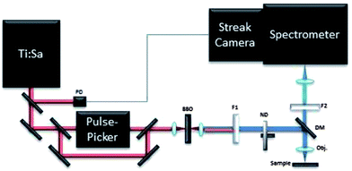 | ||
| Fig. 2 TRPL setup. PD: photodiode; BBO: type I β-barium borate crystal; F1: low pass filter; F2: high pass filter; ND: neutral density attenuator; DM: dichroic mirror; obj: microscope objective. | ||
The light is then coupled to a home-built epi-fluorescence microscope equipped with a suitable objective and focused on the sample. Light was focussed onto the sample surface through a long working distance 5× microscope objective (NA 0.15), leading to a typical irradiance of 0.7 W cm−2. The luminescence emitted by the sample is collected with the same objective and separated from the excitation light through a dichroic mirror (T455lp, Chroma Technology Corp.) and a long pass filter with cut-off at 455 nm (Comar Optics Inc.). The luminescence is then focused into the entrance slit of an imaging spectrometer (focal length 300 mm, f/3.9, 50 lines per mm grating, Acton SP2300, Princeton Instruments) with a spectral resolution of 1 nm.
The spectrometer is coupled to a streak camera detection system (C5680, Hamamatsu) with an extremely high temporal resolution of 2.5 ps when working in synchroscan operation mode at 80 MHz. In order to study time decays longer than a few ns, a slow sweep acquisition mode is employed, achieving a maximum temporal resolution of about 50 ps, which is not better than 1% of the acquired temporal window. Measurements in slow sweep mode are carried out at the maximum repetition rate of 2 MHz.
 | (1) |
The relative weight (Aiτi%) of the i-th component is calculated using eqn (2), which takes into account the number of photons emitted by each component with respect to the whole emission.
 | (2) |
2.5 X-Ray fluorescence spectroscopy
X-ray fluorescence (XRF) analysis was performed with a portable EDXRF spectrometer (Elio Spectrometer, XGlab srl, Milan, Italy). The instrument permits the detection of elements from Na to U, with the field of analysis extending between 1 and 40 keV.X-ray radiation is generated using an Rh tube, with an electron accelerating voltage from 10 to 50 kV and a filament current from 5 μA to 200 μA. Beam focusing with a suitable collimator yields a spot size on the sample of 1 mm in diameter. A large area Silicon Drift Detector (SDD), with an active area of 25 mm2 and a 12 μm beryllium window, is used as the detection unit. The typical energetic resolution is below 135 eV on the Mn-Kα fluorescence line and the typical peak to background ratio is of the order of 10![[thin space (1/6-em)]](https://www.rsc.org/images/entities/char_2009.gif) 000. For semi-quantitative analysis, approximately the same amount of material was irradiated for the same time, with the same geometric conditions and experimental settings (current and voltage) of the X-ray tube.
000. For semi-quantitative analysis, approximately the same amount of material was irradiated for the same time, with the same geometric conditions and experimental settings (current and voltage) of the X-ray tube.
3. Results
3.1 Microscopy and chemical characterization
The pigments are finely ground powders. The average diameter of the particle was evaluated using an optical Leica DMRE microscope in dark field modality, equipped with a digital camera. The images were post-processed and the particle size was evaluated to be between 1.5 and 3 μm. For this reason, quantum confinement can be excluded and the different colours of the pigments are attributed to bulk absorption.In order to verify the chemical composition provided by purchasers (listed in Table 1), semi-quantitative XRF analysis was performed on bulk materials. As an example, the XRF spectrum of sample KP3 is reported in Fig. 3 together with the relative amounts of the elements detected in the KP series, calculated by normalizing the counts of the maximum Kα line in the series.
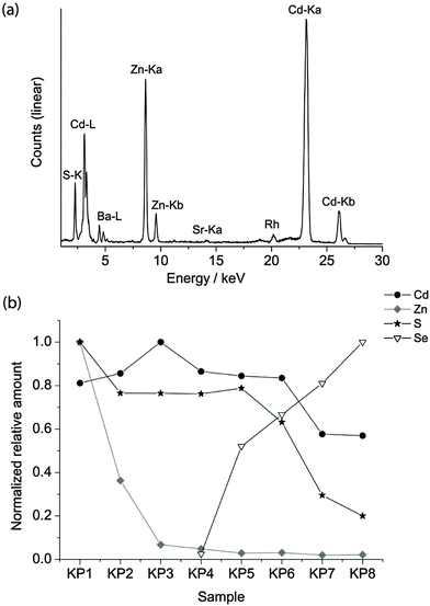 | ||
| Fig. 3 XRF spectrum of KP3 (a), the relative amount of Cd, Zn, S and Se in the KP series normalised to the maximum signal of the dataset (b). | ||
The composition varies from a high concentration of Zn in the lighter yellow shadows to an increase in the concentration of cadmium in the dark yellow and Se in the red hues. XRF of the WN series revealed the presence of Sr, Ba and occasionally K. Since Ba is present in the greatest concentrations in the lighter shadows, it is possible that lithopone white (ZnS + BaSO4) was used to obtain this hue.2
3.2 Spectral properties of band edge emission
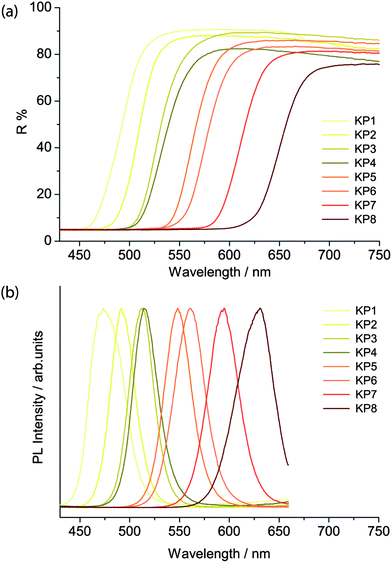
The band edge energies were evaluated through the reflectance and emission spectra, obtained respectively with the spectrophotometer and the laser-induced luminescence spectrometer. The latter was employed by exciting the sample in a pulsed regime with a irradiance of 5 mW cm−2 and acquiring the spectra with a 10 ns temporal gate, in order to select only the fast emission from the band gap and remove any slow emission from trap states.As reported by Anglos et al.,9 the diffuse reflectance spectra in the visible region show the typical semiconductor sigmoidal shape (Fig. 4a), while the band gap emission energy changes from 475 nm in the lighter yellow shadows to 630 nm in the deeper reds for the KP series (Fig. 4b), and from 490 to 590 nm in the WN series. WN3 and WN4 present two emissions, ascribed to the two different compounds present in the pigment mixtures (see Table 1).
3.3 Time-resolved photoluminescence spectroscopy of the band gap and trap state emissions
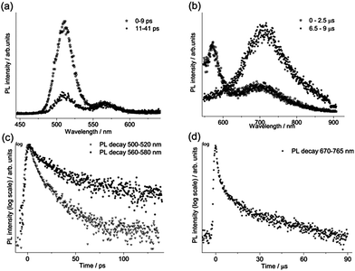
For each sample, the fast emission from the band edge and the much slower emission from the first deep trap state were measured by changing the streak camera modality from synchroscan to slow sweep mode. In the first case the repetition rate of the light pulses is 80 MHz with a temporal window acquisition of 160 ps, which leads to the best available temporal resolution of 2 ps. In the second case a temporal window of 100 μs (temporal resolution of about 1 μs) is employed and the laser repetition rate is reduced to 10 kHz.An example of the decay properties of cadmium pigments is shown in Fig. 5, where gated spectra and decay profiles of sample WN4 for both the fast (0–160 ps) and longer (0–100 μs) acquisition modes are shown. The early and late gated spectra, acquired in two narrow picosecond temporal windows following laser excitation, allow the isolation of the fast emission from the band edge, which, for the selected sample, has two distinct peaks ascribable to the two different cadmium compounds present in the pigment (Fig. 5a). The band edge emission from the two cadmium crystals can be well discriminated even in terms of temporal behaviour, CdS emission (at higher energy) dumping more rapidly than CdSe, as can be inferred from the late gated spectrum of Fig. 5a and more clearly from the extrapolated temporal decay profiles (Fig. 5c). Similarly, Fig. 5b and d present the emission properties from the first trap state, which are well isolated from the band edge emission in the late gated spectrum acquired 6.5 μs after laser excitation and characterized by a broad emission peaked at 700 nm, whereas the extrapolated decay profile suggests a microsecond lifetime. The band edge emission properties of all samples were fitted with a bi-exponential model and the results are summarized in Table 2 in terms of emission peak (λPeak), lifetime (τ), relative weights (Aτ%) and τ average. In addition the weighted average lifetime has also been calculated. This last parameter correlates with the chemical composition of pigments; cadmium sulphide pigments (in bold text) have a shorter lifetime and a predominance of the fast component in comparison to those based on cadmium sulphoselenides (in normal text). WN4 and WN5 samples, being a mixture of the two cadmium crystals, show two well-separated band edge emissions, each with distinct decay behaviour evaluated in different spectral ranges.
| Sample | Band edge emission | Trap state emission | ||||||||
|---|---|---|---|---|---|---|---|---|---|---|
| λ Peak/nm | τ 1/ps | τ 2/ps | A 2 τ 2% | τ Average | λ Peak/nm | τ 1/μs | τ 2/μs | A 2 τ 2% | τ Average | |
| a Second band edge emission of WN4 and WN5. b Unreliable fit due to noisy data. | ||||||||||
| KP1 | 476 | 3.8 | — | — | 3.8 | 660 | 1.4 | 16.4 | 72.4 | 10.9 |
| WN1 | 490 | 4.3 | 16.6 | 42.5 | 9.5 | 680 | 1.4 | 15.9 | 73.7 | 10.7 |
| KP2 | 492 | 4.7 | 34.6 | 18.8 | 10.3 | 690 | 1.5 | 17.5 | 83.7 | 13.4 |
| WN5 | 506 | 4.1 | 19.1 | 62.4 | 13.5 | 705 | 1.2 | 14.8 | 84.3 | 11.5 |
| WN3 | 509 | 4.3 | 19.4 | 51.7 | 12.1 | 720 | 1.2 | 23.4 | 78.0 | 17.3 |
| WN4 | 509 | 4.5 | 19.5 | 44.3 | 11.1 | 702 | 1.6 | 21.2 | 79.2 | 15.5 |
| KP3 | 512 | 3.3 | 20.5 | 30.1 | 8.5 | 705 | 1.6 | 21.4 | 81.8 | 16.2 |
| WN2 | 512 | 4.2 | 17.1 | 52.3 | 10.9 | 705 | 1.4 | 17.6 | 79.3 | 12.9 |
| KP4 | 514 | 3.2 | 22.4 | 29.8 | 8.9 | 710 | — | — | — | — |
| KP5 | 548 | 6.5 | 38.6 | 89.0 | 35.1 | 720 | 2.0 | 12.8 | 76.0 | 8.2 |
| KP6 | 560 | 6.9 | 32.1 | 84.5 | 28.2 | 732 | 1.5 | 11.9 | 72.2 | 7.5 |
| WN4a | 566 | 3.4 | 22.4 | 91.7 | 20.8 | — | — | — | — | — |
| WN5a | 567 | 6.3 | 37.5 | 84.5 | 32.6 | — | — | — | — | — |
| WN6 | 573 | 4.9 | 25.5 | 84.0 | 22.2 | 705 | 1.8 | 19.8 | 77.8 | 14.0 |
| WN7 | 583 | 5.3 | 28.1 | 86.1 | 24.9 | 765 | 2.0 | 17.3 | 78.3 | 12.0 |
| WN8 | 587 | 5.7 | 29.9 | 85.6 | 26.4 | 770 | 2.0 | 14.4 | 79.5 | 9.9 |
| KP7b | 594 | 10.7 | 60.3 | 91.4 | 56.1 | 770 | 2.4 | 19.6 | 71.4 | 12.3 |
| KP8 | 629 | 7.5 | 30.6 | 81.4 | 26.4 | 802 | 1.6 | 10.8 | 66.60 | 6.1 |
The first deep trap state emission maximum shifts to longer wavelengths with the band edge emission wavelength, in agreement with results reported by Thoury et al.5 The measured decay curves were fitted with a bi-exponential model and the resulting emission lifetimes (τ) and relative weights (Aτ%) are reported in Table 2. The emission lifetimes, which are on the order of tens of microseconds for the most important component (τ2), do not depend on the chemical composition of samples.
3.4 Spectral and lifetime properties of emissions at different excitation irradiance
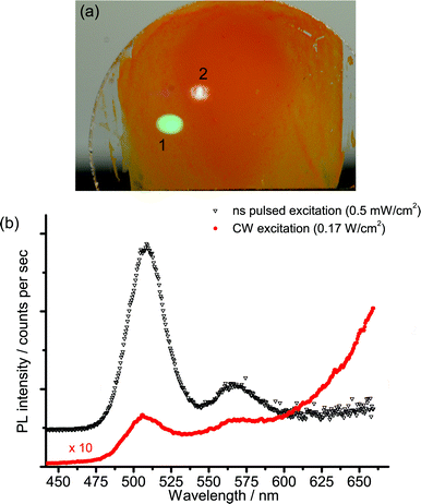
The strong non-linear behaviour that has been reported for Cd-based nanocrystals17,19,20 led us to investigate the spectral and kinetic emission properties of the cadmium pigments at different values of irradiance on samples.The investigation was first made with the laser-induced luminescence spectrometer with CW excitation by changing irradiance from 60 to 1700 W cm−2. A noticeable variation in the emission spectrum with increasing irradiance was observed: the emission from the band edge is promoted with respect to trap state emissions at higher power densities. A detailed investigation of this phenomenon was performed on sample WN1 (Fig. 6) which demonstrates a minor saturation of trap state emission with irradiance and a non-linear dependence for band edge emission, which is characterized by linear and quadratic terms. A more dramatic effect deriving from the non-linear behaviour with irradiance was observed when the nanosecond 355 nm Q-switched laser was used to excite the samples. The excitation power over pulse duration was about 50 kW cm−2, while the pulses are, at the same time, much longer than the band edge emission and much shorter than the trap state emission (see TRLP data), and so we consider this regime as quasi-CW. Under these conditions the luminescence emission at short wavelength, which has been ascribed to the band edge, is strongly enhanced while the trap state emission at long wavelength is severely dumped. This effect can be immediately appreciated with reference to Fig. 7 that shows (a) the emissions and (b) the spectra from sample WN3 excited with the nanosecond (spot 1) and the CW (spot 2) laser sources. The collimated beam of the CW laser delivers irradiance (170 W cm−2) on the sample that favours the emission from the trap state. In contrast, by employing a low-repetition rate (100 Hz) pulsed laser (100 Hz, 50 μJ cm−2), the green band edge emission prevails over the trap emission, due to the high peak irradiance (50 kW cm−2), even though the average irradiance is much smaller (5 mW cm−2).
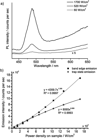 | ||
| Fig. 6 PL spectra of WN1 following CW excitation at three different values of irradiance (a); the PL band edge (490 nm) and trap state emission intensity (650 nm) as a function of irradiance (b). | ||
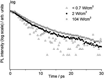
TRPL measurements on the same sample (WN1) were also carried out by changing the irradiance from less than 0.7 W cm−2 to 350 W cm−2. For this purpose, the laser beam was focused using a 10× long working distance microscope objective. The high temporal resolution range (160 ps) was adopted in order to observe possible temporal variation of the fast emission from the band edge. In Fig. 8 the temporal profiles at three different values of irradiance are reported showing a slower decay upon increasing irradiance on the sample. In the case of the lowest irradiance we observe mono-exponential behaviour with a lifetime of about 3.3 ps. This value of lifetime is comparable with the temporal resolution of the system, hence it is considered as an upper limit. With increasing irradiance, the temporal profile is characterized by a bi-exponential decay, with components close to 5 ps and 20 ps and the relative weight of the slower component increases with irradiance. For values of irradiance higher than 100 W cm−2 no further increase in lifetime is observed and the relative amplitude of the faster decay settles to 88%.
4. Discussion
The decay kinetics of photoluminescence emission from a series of commercial Cd-based pigments have been studied and they demonstrate variation which is ascribed to differences in composition and synthesis.Band edge emission shows a fast picosecond decay related to pigment composition, with an average lifetime varying around 10 ps for the (Zn,Cd)S compounds (with the exception of KP1) and from 20 to 35 ps for Cd(Se,S) pigments (with the exception of KP7). The extremely fast decay of photoluminescence indicates that the visible emission detected in Cd pigments is influenced by non-radiative decay paths likely related to shallow or deep trap states, which basically determine the free carrier lifetime, which has also been reported for Cd(S,Se) doped glasses.23 Interestingly, the measured lifetimes are in partial agreement with those that have been reported in the past for CdS single crystals, where a fast decay time (τ < 100 ps) was measured in samples with mechanically damaged surfaces and a longer lifetime (τ > 1 ns) was detected in samples subjected to chemical etching.24,25 This variation in lifetime with crystal surface characteristics indicates that the band edge emission decay is influenced by surface crystal defects, which introduce intermediate trap state levels.
In contrast to the fast decaying band-edge emission, the first deep trap state emission shows a lifetime ranging from 10 to 25 μs, which varies widely in different samples, without showing any clear correlation with the chemical composition. Trap states are typically related to defects and vacancies of the crystal matrix,12 hence the variation in emission lifetime among samples can be associated with modifications of crystal structures introduced during pigment synthesis, pigment mechanical grinding or initial surface degradation processes. Indeed, it has been reported that mechanical grinding of CdS and CdSe crystals induces randomization of the crystal structure.26
Non-linear behaviour was demonstrated by PL experiments at different irradiance, both in CW and with short pulses. Measurements have shown that the ratio between the band edge and the trap state emission intensity depends on the excitation intensity. These findings confirm that the mechanism for carrier recombination in cadmium pigments is highly influenced by electron trapping in deep trap states. Similar behaviour has already been reported for small Cd(S,Se) crystallites by Kull et al. who also proposed a rate equation model for the carrier density in the conduction band and in the trap states.18 A similar model is proposed here to interpret the experimental findings.
The density of free carriers (n) at the edge of the conduction band is described by eqn (3)
 | (3) |
 | (4) |
It has been reported that electron trapping is a very fast process in cadmium-based semiconductors,20,27 while the radiative decay is negligible, owing to the very low quantum yield. Hence assuming a Dirac delta function for the excitation, at low intensity, the trapping time 1/C drives the fastest free carrier decay (few picoseconds), while the other terms in eqn (3) are almost negligible:
 | (5) |
Yet, when increasing the excitation intensity, nT also increases, leading to partial trap saturation. Carrier density n also increases and experiences a multi-exponential dumping, since other terms in eqn (3), mostly n/τ, become significant, leading to a longer average lifetime, in agreement with the slower kinetics of the emission observed in TRPL measurements at higher fluence (Fig. 8). On the other hand, the recombination of trap states can be observed through the red-NIR luminescence, which shows a microsecond decay.
Steady state measurements complement information provided by time-resolved data: in fact, at low excitation irradiance, the model predicts severe quenching of the band edge emission, while the saturation of trap states, which takes place at high irradiance, accounts for a non-linear increase of the blue-green emission (Fig. 6). Finally, nanosecond Q-switch pulses are likely to completely saturate the trap states, owing to their slow decay time, thus providing a strong increase in band edge emission (Fig. 7).
The strong dependence of pigment emission on excitation irradiance has a practical implication, which should be taken into account when studying real works of art. Luminescence analysis in conservation science is typically performed by employing low-power CW sources (such as Wood or xenon lamps for traditional UV-induced photography or spectrofluorimetry analysis, respectively), which mostly induce emissions from deep trap states (Fig. 7). In order to observe the band edge emission, high-power CW light sources could be employed (with irradiance higher than 100 W cm−2). Yet, this might induce thermal and photo-oxidative damages to paintings. Alternatively, a simple pulsed nanosecond laser source can be employed for more efficiently inducing the radiative emission from the band edge.9,10 It has been shown that a photon fluence of 50 μJ cm−2, which is well below typical damage thresholds,28 leads to an effective saturation of trap states followed by strong emission from the edge of the conduction band.
This observation suggests that portable spectrofluorimetry with nanosecond pulsed laser excitation is a valuable technique for inspecting the band edge emission from semiconductor pigments in real works of art. The combined use of a gated spectrometer can be of further help in removing the much dimmer slow emissions from trap states9,29 as also observed in present paper (Section 3.2).
5. Conclusions
For the first time we report the characterization of the luminescence decay kinetics from a series of commercial Cd-based pigments. The physical interpretation of the measured lifetimes is not trivial and suggests that the mechanism for carrier recombination is not only ruled by electron–hole recombination, but also highly influenced by electron trapping in deep trap states.Lifetime measurements provide a means of understanding such a mechanism and might be relevant to detect physical changes in these semiconductor pigments. We have shown that the features of the band edge emission (lifetime and the spectrum) are related to the chemical composition of pigments and can be used for discriminating among them, while the trap state emission is unspecific and is likely related to crystal defects introduced during pigment synthesis. CW spectroscopy typically used to inspect works of art can hardly access the band edge emission. To overcome this limitation, we have shown that a portable nanosecond laser source can be used to effectively excite the luminescence of cadmium-based pigments.
In the future, the same approach will be employed for assessing the dependence of emission features on pigment degradation and oxidation phenomena, considering both artificially aged samples, historical Cd-based pigments and real paintings. Moreover, further studies will be carried out to investigate the photo-physical behaviour of other semiconductor modern pigments.30
Acknowledgements
Research was partially funded through the Italian Ministero dell'Istruzione, dell'Università e della Ricerca (MIUR) Futuro in Ricerca (FIRB) project: “Tecniche pittoriche, critica delle varianti e problemi conservativi. Tra Futurismo e ritorno al classico (1910–1922)” (RBFR12PHL4_003).Notes and references
- B. Leone, A. Burnstock, C. Jones, P. Hallebeek, J. J. Boon, and K. Keune, in 14th triennial meeting, The Hague, 12–16 September 2005: preprints (ICOM Committee for Conservation), ed. I. Verger, Earthscan Ltd., London, United Kingdom, 2005, pp. 803–813 Search PubMed.
- I. Fiedler and M. Bayard, in Artists' Pigments: A Handbook of Their History and Characteristics, ed. R. L. Feller, Cambridge University Press and National Gallery of Art, Cambridge, 1986, pp. 65–108 Search PubMed.
- J. L. Mass, R. Opila, B. Buckley, M. Cotte, J. Church and A. Mehta, Appl. Phys. A: Mater. Sci. Process., 2012, 111, 59–68 CrossRef.
- F. Rosi, C. Miliani, C. Clementi, K. Kahrim, F. Presciutti, M. Vagnini, V. Manuali, A. Daveri, L. Cartechini, B. G. Brunetti and A. Sgamellotti, Appl. Phys. A: Mater. Sci. Process., 2010, 100, 613–624 CrossRef CAS.
- M. Thoury, J. K. Delaney, E. R. D. La Rie, M. Palmer, K. Morales and J. Krueger, Appl. Spectrosc., 2011, 65, 939–951 CrossRef CAS PubMed.
- D. Comelli, A. Nevin, A. Brambilla, I. Osticioli, G. Valentini, L. Toniolo, M. Fratelli and R. Cubeddu, Appl. Phys. A: Mater. Sci. Process., 2011, 106, 25–34 CrossRef.
- G. Van der Snickt, J. Dik, M. Cotte, K. Janssens, J. Jaroszewicz, W. De Nolf, J. Groenewegen and L. Van der Loeff, Anal. Chem., 2009, 81, 2600–2610 CrossRef CAS PubMed.
- T. Miyoshi, M. Ikeya, S. Kinoshita and K. Takashi, Jpn. J. Appl. Phys., 1982, 21, 1032–1036 CrossRef CAS.
- D. Anglos, M. Solomidou, I. Zergiotti, V. Zafiropulos, T. Papazoglou and C. Fotakis, Appl. Spectrosc., 1996, 50, 1331–1334 CrossRef CAS.
- I. Borgia, R. Fantoni, C. Flamini, T. M. Di Palma, A. G. Guidoni and A. Mele, Appl. Surf. Sci., 1998, 95–100 CrossRef CAS.
- P. K. Weimer, in Proceedings of the IRE, 1962, pp. 1462–1469 Search PubMed.
- V. Babentsov, J. Riegler, J. Schneider, O. Ehlert, T. Nann and M. Fiederle, J. Cryst. Growth, 2005, 280, 502–508 CrossRef CAS PubMed.
- N. Chestnoy, T. D. Harris, R. Hull and L. E. Brus, J. Phys. Chem., 1986, 90, 3393–3399 CrossRef CAS.
- U. Woggon, in Tracts in Modern physics, Springer, Berlin, 1997, vol. 136 Search PubMed.
- L. Qu and X. Peng, J. Am. Chem. Soc., 2002, 124, 2049–2055 CrossRef CAS PubMed.
- P. Roussignol, D. Ricard, J. Lukasik and C. Flytzanis, J. Opt. Soc. Am. B, 1987, 4, 5 CrossRef CAS.
- P. Verma, G. Irmer and J. Monecke, J. Phys.: Condens. Matter, 2000, 12, 1097–1110 CrossRef CAS.
- M. Kull and J.-L. Coutaz, J. Opt. Soc. Am. B, 1990, 7, 1463–1472 CrossRef CAS.
- S. S. Yao, C. Karaguleff, A. Gabel, R. Fortenberry, C. T. Seaton and G. I. Stegeman, Appl. Phys. Lett., 1985, 46, 801–802 CrossRef CAS.
- M. Tomita and M. Matsuoka, J. Opt. Soc. Am. B, 1990, 7, 1198–1203 CrossRef CAS.
- S. Shionoya and W. H. Hen, Phosphor Handbook, Boca Raton (FL), 1997 Search PubMed.
- L. De Trizio, M. Prato, A. Genovese, A. Casu, M. Povia, R. Simonutti, M. J. P. Alcocer, C. D’Andrea, F. Tassone and L. Manna, Chem. Mater., 2012, 24, 2400–2406 CrossRef CAS.
- J. P. Zheng and H. S. Kwok, Appl. Phys. Lett., 1989, 54, 1–3 CrossRef CAS.
- M. Evenor, S. Gottesfeld, Z. Harzion, D. Huppert and S. W. Feldberg, J. Phys. Chem., 1984, 88, 6213–6218 CrossRef CAS.
- Z. Harzion, S. Gottesfeld, D. Huppert and N. Croitoru, J. Electroanal. Chem., 1983, 150, 571–581 CrossRef CAS.
- K. Durose, A. T. Fellows, A. W. Brinkman, G. J. Russell and J. Woods, J. Mater. Sci., 1985, 20, 3783–3789 CrossRef CAS.
- M. C. Nuss, W. Zinth and W. Kaiser, Appl. Phys. Lett., 1986, 49, 1717–1719 CrossRef CAS.
- S. Georgiou, V. Zafiropulos, D. Anglos, C. Balas, V. Tornari and C. Fotakis, Appl. Surf. Sci., 1998, 127–129, 738–745 CrossRef CAS.
- D. Comelli, C. D'Andrea, G. Valentini, R. Cubeddu, C. Colombo and L. Toniolo, Appl. Opt., 2004, 43, 2175–2183 CrossRef.
- C. Clementi, F. Rosi, A. Romani, R. Vivani, B. G. Brunetti and C. Miliani, Appl. Spectrosc., 2012, 66, 1233–1241 CrossRef CAS PubMed.
| This journal is © The Royal Society of Chemistry 2014 |

