 Open Access Article
 This Open Access Article is licensed under a Creative Commons Attribution-Non Commercial 3.0 Unported Licence
Controlling the microstructure of poly(vinylidene-fluoride) (PVDF) thin films for microelectronics
Mengyuan
Li
*a,
Ilias
Katsouras
b,
Claudia
Piliego
b,
Gunnar
Glasser
b,
Ingo
Lieberwirth
b,
Paul W. M.
Blom
b and
Dago M.
de Leeuw
b
aZernike Institute for Advanced Materials, University of Groningen, Nijenborgh 4, 9747 AG, Groningen, The Netherlands. E-mail: mengyuan.li@rug.nl
bMax Planck Institute for Polymer Research, Ackermannweg 10, 55128, Mainz, Germany
First published on 23rd September 2013
Abstract
PVDF thin films prepared under standard processing conditions have a cloudy appearance and are notoriously rough, which prevent microelectronic and photonic applications. On the other hand, high optical quality, smooth films can be prepared either at low relative humidity or at high substrate temperature. Here we systematically investigate the morphology of PVDF thin films by varying the processing conditions. Films are characterized by SEM and AFM and by measurements of clarity, haze and absorption. We show that the cloudy appearance is due to vapor-induced phase separation (VIPS) as is well-documented for the formation of PVDF membranes. Formation of opaque thin films is a general problem of any ternary polymer/solvent/non-solvent system where a high boiling point solvent is used that is fully miscible with a non-solvent, here water from the ambient.
1. Introduction
Poly(vinylidene-fluoride) (PVDF) films are used in a wide variety of applications such as hydrophobic coatings in architecture, membranes for microfiltration, gas separation or water desalination, and as ferroelectric memories for data storage. Each application has its own requirements on the microstructure. For instance, PVDF membranes are about 250 μm thick films characterized by an open porous structure with a high specific surface area. On the other hand, ferroelectric transistors require much thinner films, of about 100 nm, that are pinhole-free to prevent electrical shorts.Polymer-based micro-porous membranes are typically prepared by controlled phase separation of polymer solutions into two phases, one with a high- and one with a low-polymer content.1,2 The concentrated phase solidifies shortly after phase separation and forms an asymmetric membrane, meaning that the pore size varies from top to bottom. The phase separation can be induced by thermal energy or by incorporation of a non-solvent. PVDF membranes, widely used due to their good chemical and thermal stability,3 can be prepared by wet-inversion or immersion precipitation. Right after casting, a thick PVDF film is immediately immersed in a bath of a non-solvent that is fully miscible with the casting solvent. The phase separation then occurs due to exchange of solvent and non-solvent. The rapid mass transfer however can yield macro-voids that limit the functionality of the membrane.4 To circumvent this problem and for applications that require larger surface pores, vapor-induced phase separation (VIPS) is typically applied. Here, a PVDF film is cast from N,N-dimethylformamide (DMF), a high boiling point solvent that evaporates slowly. Water vapor from humidified air is fully miscible with DMF and penetrates the wet film by diffusion. The evaporation of DMF is slower than the intake of water. Since water is a non-solvent for PVDF, phase separation occurs. Highly porous PVDF membranes with pore diameters ranging from microns to sub-microns can then be prepared. The phase separation itself is a complex interplay between the equilibrium thermodynamics and mass transfer kinetics, which is, nonetheless, well understood.5,6
In contrast, microelectronic applications such as ferroelectric memories for data storage require much thinner films of about 100 nm. The films should be pinhole-free to prevent formation of electrical shorts. However, PVDF films have a “cloudy” appearance and are notoriously rough.7–12 The porosity of PVDF films can be so pronounced that it prohibits electrical characterization.7,8 Although smooth ferroelectric films of 300 nm or more could be prepared by thermal annealing directly after deposition under ambient conditions, thinner films as required for low-voltage operation still crystallize in a porous film.9 In addition, it has been reported that the PVDF film surface resulting from spin-coating is too rough to be applicable in microelectronics.10 A breakthrough would be the realization of homogeneous and smooth thin PVDF films with roughness in the nanometer regime. To this end, the origin of cloudiness and surface roughness needs to be elucidated.
Cloudy films were first observed in a study of spin-coating of negative electron-beam resist, where the hygroscopic solvent DMF was used.13 The morphology of the scattering films originates from the precipitation of the polymer caused by moisture in the ambient atmosphere. The cloudy appearance can be prevented by spin-coating in a nitrogen atmosphere13 or by using an elevated substrate temperature.14 Smooth films of PVDF have been reported using humidity-controlled spin-coating.10,11 Two extreme examples of films prepared at high- and low humidity are presented in Fig. 1. We demonstrate that optical-quality smooth films can be prepared either at low relative humidity or at elevated substrate temperature.
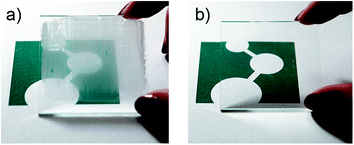 | ||
| Fig. 1 Optical quality of PVDF thin films. The photographs show the logo of the Max Planck Institute for Polymer Research as seen through thin films of PVDF. The 1 μm thick films were deposited on glass substrates at room temperature at a relative humidity of (a) 60% and (b) 0%. At low humidity an optically clear, dense, smooth film is obtained. At high relative humidity the film has a cloudy appearance. The film is porous with a roughness that is comparable to the film thickness. | ||
We systematically investigate the morphology and the macroscopic optical properties of nominal 1 μm thin PVDF films as a function of substrate temperature and relative humidity. The roughness and microstructure of the films are characterized by atomic force microscopy (AFM) and scanning electron microscopy (SEM) measurements. The optical properties are characterized by haze and clarity measurements. The absorbance as a function of wavelength is quantitatively related to the surface roughness. The data extracted are explained using compositional trajectories through the isothermal ternary phase diagram of the PVDF/DMF/water system that was previously derived to analyze PVDF membrane morphology. The generality for formation of cloudy and scattering thin films of any polymer/solvent/non-solvent system is discussed.5,6
2. Experimental
PVDF (Mw = 180 kg mol−1) was purchased from Sigma-Aldrich and used as received. PVDF has a very limited solubility in common organic solvents. PVDF is typically dissolved in polar solvents such as DMF, dimethyl sulfoxide (DMSO), N-methylpyrrolidone (NMP) or dimethylacetamide (DMAc). Here, PVDF was dissolved in DMF, typically at 10 wt%. The dissolution temperature of 100 °C is above the critical dissolution temperature15 of about 40 °C to ensure thermodynamic equilibrium. At low temperature very small crystallites exist, due to partial dissolution or refolding of the polymer chains, which serve as nuclei when the solution is recrystallized. The nuclei cannot be destroyed with longer dissolution time, but only by raising the dissolution temperature.15 Spin-coated PVDF films can be inhomogeneous over the substrate. In agreement with literature reports16 films can be opaque in the center and transparent at the edges. To fabricate uniform films, wire-bar (Meyer rod) coating was used (K202 control coater, RK Print). An additional advantage of wire-bar coating is the accurate control of the substrate temperature that was varied between 20 °C and 120 °C. Thoroughly cleaned glass was used as a substrate. To set the relative humidity between 0% and 60%, a Perspex® box was built around the coater. The inside was flushed with humidified nitrogen for about half an hour until the set relative humidity was constant. We note that 0% does not mean completely water free. The actual concentration is only below 0.01%, which is the detection limit of the hygrometer. In the rest of the manuscript we use for short 0%.The thickness and roughness of PVDF films were measured with a surface profilometer. The topography was investigated with an AFM (Nanoscope Dimension 3100, Bruker). The microstructure was investigated with a low voltage SEM (LVSEM) using a Zeiss 1530 Gemini or a Hitachi SU8000 microscope for different resolutions. Micrographs were acquired at an accelerating voltage of 400 V. Samples were not coated.
The crystal structure of the films was characterized by grazing incidence X-ray diffraction, using a Philips X'pert MRD diffractometer. All PVDF films, irrespective of the substrate temperature and relative humidity, crystallized in the paraelectric α-phase.12
The standard (industrial) optical characteristics haze and clarity were measured for the thin films with a “Haze-gard plus” instrument (BYK Gardner GmbH, Germany). In this test, haze is commonly defined as the portion of visible light that is scattered at wider angles (2.5° < θ < 90°) and is a measure for the turbidity of a sample. Clarity, on the other hand, usually refers to the scattering contribution at small angles (θ < 2.5°) and is related to the sharpness of an object when viewed through the sample (cf. manual of Haze-gard plus). Steady-state UV-vis absorption spectra were measured using a Perkin-Elmer Lambda 25 spectrophotometer.
3. Characterization of PVDF thin films
The thickness and roughness as a function of substrate temperature are presented in Fig. 2 for films fabricated at a relative humidity between 0% and 60%. The solid lines are a guide to the eye. At 0% relative humidity the layer thickness is about 1 μm, and independent of the substrate temperature. These benchmark films are extremely smooth; the rms roughness is less than 10 nm. It indicates that the films are dense. Fig. 2 shows that the layer thickness and roughness systematically increase with increasing humidity and decreasing substrate temperature. Each as-cast wire-bar coated film contains the same amount of solution and therefore the same amount of PVDF. The measured increase in layer thickness implies that the films are not dense but porous, as corroborated by SEM measurements.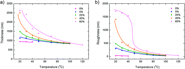 | ||
| Fig. 2 Topography of PVDF thin films. PVDF thin films were prepared by wire-bar coating as a function of substrate temperature between 20 °C and 120 °C. The relative humidity was varied between 0% and 60%. (a) The layer thickness and (b) the rms roughness were obtained from surface profilometry measurements. The solid lines are a guide to the eye. | ||
Representative SEM micrographs are shown in Fig. 3. In Fig. 3a, the films were deposited at room temperature, 20 °C, and the relative humidity was varied between 0% and 60%. The top view images are presented on the left and the corresponding cross-sections, obtained by breaking the glass substrate, on the right. The top view micrographs show that at high relative humidity the film is porous and consists of loosely connected particles of PVDF. With decreasing relative humidity, the PVDF spheres get more and more connected. At 0% relative humidity, a homogeneous dense smooth film is obtained, without any pinholes. The size of the primary particles increases with decreasing relative humidity. The corresponding cross-sections show that the spheres get flattened, more like pancakes. We note that qualitatively the same dependence on substrate temperature and humidity is found when using spin-coating as a deposition technique. However the changes in morphology are not so pronounced, due to the faster drying of spin-coated films, i.e. less intake of water.
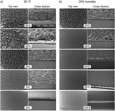 | ||
| Fig. 3 Surface morphology evolution of PVDF thin films. (a) Top view and cross-section SEM micrographs of PVDF thin films presented as a function of the relative humidity between 0% and 60%. The films were deposited at room temperature, 20 °C. The scale bars of 10 μm and 2 μm are presented in the bottom micrographs. (b) Top view and cross-section SEM micrographs of PVDF thin films presented as a function of the deposition temperature between 20 °C and 100 °C. The relative humidity was fixed at 25%. | ||
In Fig. 3b, the relative humidity was fixed at 25% and the substrate temperature was increased from 20 °C to 100 °C. Again, the top view figure shows that at low temperature the film is porous and consists of loosely connected particles of PVDF. The corresponding cross-section shows monodisperse hemispheres with a diameter of about 3 μm. The PVDF spheres coalesce with increasing substrate temperature. Above about 90 °C a homogeneous dense smooth film is obtained. In contrast to Fig. 3a, the diameter of the primary spheres remains approximately constant. Actually the intermediate SEM pictures are characteristic of the growth of thin films by coalescence processes in the post-nucleation stage.17 This type of growth is also characteristic of thin evaporated metal films on non-wetting surfaces. In the initial stage nuclei are formed that grow by capturing ad-atoms. In the subsequent coalescence stage touching nuclei transform into a single entity with lowering of the surface free energy as the driving force. In the final stage the individual nuclei grow at a faster rate than that of the coalescence events, leading to more and more continuous films with separation of the nuclei by voids or grain boundaries. Here the pictures of Fig. 3 show phenomenologically the same behavior albeit that the mechanism, phase separation, is completely different.
To investigate the primary PVDF particle size we performed AFM measurements. Representative height images for a relative humidity of 25% and 60% are presented in Fig. 4. At low substrate temperature the films are porous and at high substrate temperature dense films are obtained. The primary particle size for the full datasets is presented in Fig. 4b. The average diameter amounts to 3 μm, similar to that extracted from the SEM micrographs shown in Fig. 3b. At elevated temperatures the diameter is humidity independent, although the shape changes with temperature from a hemisphere to a pancake. This is corroborated by calculating the power spectral density (PSD) as a function of spatial frequency from the AFM height profiles.18 This analysis reveals two correlation lengths. One length corresponds to the particle diameter, about 3 μm, while the other one depends on the substrate temperature and might be related to the size of the pores.
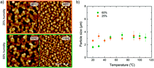 | ||
| Fig. 4 AFM topography and primary particle size. (a) Representative AFM height images for films fabricated at a relative humidity of 25% at substrate temperatures of 30 °C and 90 °C, and at a relative humidity of 60% at substrate temperatures of 50 °C and 110 °C. The films on the left are porous and the films on the right are dense and smooth. The scale bar is indicated. (b) The primary particle size for the full datasets presented as a function of substrate temperature. The average diameter amounts to about 3 μm and at elevated temperatures it is independent of relative humidity. | ||
The microscopic details of the microstructure are reflected in the optical properties. Therefore we measured the absorption as a function of wavelength. The spectra of films deposited at a humidity of 0%, 5% and 60% for representative substrate temperatures between 20 °C and 120 °C are presented on a double logarithmic scale in Fig. 5.
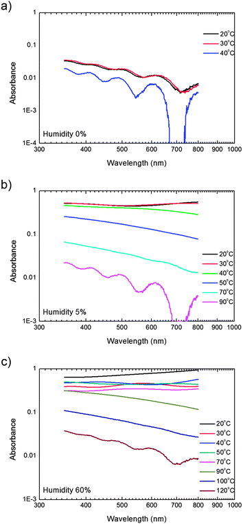 | ||
| Fig. 5 Optical absorption. UV-vis absorption as a function of wavelength on a double logarithmic scale of PVDF thin films deposited at various substrate temperatures at a relative humidity of (a) 0%, (b) 5% and (c) 60%. | ||
The films prepared at low humidity or at high substrate temperature show interference fringes, which demonstrates that these films are extremely smooth. It is well known that any interference effect is immediately destroyed when the film thickness is not uniform or when the layer is rough. The smoother the film, the lower the absorbance and the more pronounced the interference fringes. We note that from the interference fringes either the layer thickness or the index of refraction can be determined.19
PVDF has a band gap of about 6 eV.20 The transmission loss therefore cannot be due to bulk PVDF absorption but is due to light scattering instead. The roughness increases with increasing humidity and decreasing substrate temperature. Fig. 5 shows that concomitantly the absorption increases. Furthermore, Fig. 5 shows that the dispersion is described by straight lines, meaning that the absorption decreases with the square root of the wavelength, indicative of Mie scattering.
To quantitatively describe the optical absorption coefficient, α, we use a theory developed to evaluate the optical properties of microcrystalline silicon thin films and solar cells.21 The formalism for the surface and bulk light scattering has been evaluated from transmittance, reflectance and absorbance measurements over a broad spectral region.21 The light scattering occurs both at bulk inhomogeneities, such as voids, and at the surface. Both effects lead to the attenuation of the specular reflected and transmitted beams and to an enhancement of the absorption. The thin films investigated exhibited an rms roughness as measured with an AFM between 10 and 40 nm. Because the Fourier transform analysis of the AFM data revealed a small correlation distance, the scalar scattering theory for random rough surfaces with a small correlation distance could be used.21,22 The scattering coefficient, αsc, could therefore be related to the rms surface roughness, σrms, as follows:21
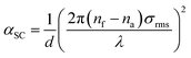 | (1) |
Here we apply this equation for the PVDF films. We assume that the absorption coefficient is dominated by the scattering coefficient. The calculated absorption, using a value of 1.4 for the index of refraction of PVDF,20 is presented as a function of the measured absorption in Fig. 6a. The calculations were performed at wavelengths of 400 nm, 600 nm and 800 nm. Good agreement is obtained for films with a roughness up to about 100 nm. For rougher films the aforementioned approximations do not hold and eqn (1) is not applicable.
 | ||
| Fig. 6 Analytical scattering approach. (a) The absorption calculated using eqn (1) presented as a function of the measured absorption. The calculations were performed at wavelengths of 400 nm, 600 nm and 800 nm using as input the measured rms roughness and an index of refraction for PVDF of 1.4. Only films with a roughness of up to 100 nm were analyzed. For rougher films the approximations in the derivation of eqn (1) break down. (b) Representative absorption spectra of films prepared at a humidity of 5% at various substrate temperatures, replotted from Fig. 5b. The dashed lines are calculated using eqn (1). | ||
To demonstrate the agreement we replot in Fig. 6b representative absorption spectra of films prepared at a humidity of 5% at various substrate temperatures. The dashed lines are calculated using eqn (1). Excellent agreement with the measured absorption is obtained, which is remarkable taking into account that there are no adjustable parameters. Furthermore, the agreement is extraordinary, considering that the assumption of a small coherence length is not fulfilled. From the PSD analysis of the AFM data we arrive at a coherence length of 3 μm, much larger than the wavelength of light. Why the scattering is relatively insensitive to the details of the microstructure of the PVDF films is not yet understood.
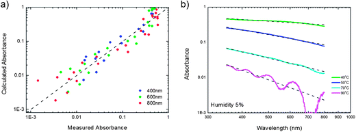
The macroscopic optical properties were characterized by measurements of clarity and haze. Haze is a measure of cloudy appearance and is defined as the fraction of transmitted light that deviates from the directly transmitted beam at angles larger than 2.5°. Haze can originate from internal or bulk scattering due to e.g. differences in refraction indices at grain boundaries, or from surface scattering. For the present 1 μm thick PVDF films, the haze is mainly caused by surface scattering. The surface haze is a complex interplay between roughness and correlation length. A general description cannot be derived because the details of the microstructure are crucial. Approximate analytical solutions for haze and clarity and the dispersion thereof have been reported, e.g. for Gaussian randomly rough surfaces with various types of correlation functions.23 Here, we measured the industrial standard haze and clarity values by using white light. The values obtained are presented in Fig. 7 as a function of substrate temperature. At 0% relative humidity the layers are smooth and the haze is therefore 0%. The haze mimics the surface roughness, cf.Fig. 2; it increases with humidity and decreases with substrate temperature. For completeness we measured the clarity or gloss. In the optical industry, gloss is used extensively to quantify the visual appearance. However, it does not show the same prominence as haze. In fact, the term clarity does not even have a rigorous scientific definition. The industrial standards are different in e.g. North America and Europe. At 0% relative humidity the layers are smooth and the clarity is 100%. The clarity decreases with relative humidity and increases with substrate temperature. We note that clarity and haze are manifestations of surface scattering. To exclude any contribution of bulk scattering, we applied an index matching liquid on top of the film. Then all films became clear and transparent. We measured a haze of about 0% and a clarity of about 100%.
 | ||
| Fig. 7 Macroscopic optical properties. (a) Haze and (b) clarity of PVDF thin films presented as a function of substrate temperature during wire-bar coating. The relative humidity was varied between 0% and 60%. Haze is a measure for the turbidity of the film, associated with loss of contrast at wide angles. Clarity is related to the sharpness of an object when viewed through the sample at small angles. | ||
4. Comparison of PVDF thin films and VIPS membranes
Vapor induced phase separation (VIPS) for membrane formation has been well-documented, and the underlying mechanisms are well-understood. Membranes are formed in a ternary system of polymer/solvent/non-solvent, where the solvent and non-solvent are fully miscible and the solvent, typically NMP, DMSO or DMF, has a high boiling point. Membranes are formed by phase separation induced by in-diffusion of the non-solvent, typically water. Examples of polymer membranes are, apart from PVDF, polysulfone24, polyetherimide25 and polyethersulfone.26 In this section we present a brief overview of the formation of PVDF membranes by VIPS. The membrane morphology is related to the compositional trajectory through the ternary phase diagram. The same phase separation occurs in wire-bar coated films. The link to the well-established field of PVDF membrane formation by VIPS explains the morphology as a function of substrate temperature and humidity. The formation of cloudy thin films comprising other ternary systems will be discussed.Morphology of the PVDF membrane formed by VIPS
The formation of PVDF membranes by VIPS is schematically depicted in Fig. 8a. A PVDF film is cast from DMF, a high boiling solvent that evaporates slowly. Water vapor from humidified air is fully miscible with DMF and penetrates the film by diffusion. The evaporation of DMF is slower than the intake of water. Because water is a non-solvent for PVDF, phase separation occurs. The phase separation itself is a complex interplay between the equilibrium thermodynamics and mass transfer kinetics, which is, nonetheless, well-understood.5,6 VIPS is elucidated in Fig. 8b where the isothermal ternary phase diagram of PVDF/DMF/H2O, as extracted by Matsuyama et al.,5,6 is schematically presented. In their work the binodal and spinodal lines were calculated from the Flory–Huggins parameters and the isothermal crystallization line was obtained from the melting point depression. The mass transfer was calculated by solving the one dimensional diffusion equations.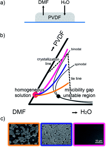 | ||
| Fig. 8 Vapor induced phase separation (VIPS) of PVDF films. (a) A PVDF film cast from DMF that evaporates slowly. Water vapor from humidified air is fully miscible with DMF and penetrates the film by diffusion leading to phase separation. (b) Schematic isothermal ternary phase diagram of PVDF/DMF/H2O. This part of the large triangular coordinate is adapted from ref. 5 and 6. The black dot is the critical point. The starting composition is given by the red dot. Three compositional trajectories of the PVDF films upon drying are represented by the yellow, purple and pink lines. (c) SEM micrographs of the corresponding morphology of the resulting PVDF films. The scale bar is indicated. | ||
To verify the calculations, Matsuyama et al. prepared 256 μm thick cast PVDF films at room temperature and kept them in controlled humidity. The membrane morphology was experimentally characterized by SEM and compared with the calculated composition path in the phase diagram.6 Good agreement was obtained.6 The morphology of the membranes could be explained from the compositional trajectories through the phase diagram of Fig. 8b. The pink line shows a case for a low relative humidity where the compositions do not cross the binodal. The wet film then is stable, liquid–liquid phase separation cannot occur and a dense microstructure is obtained. The purple line shows the hypothetical case at a higher relative humidity where the composition of the membrane crosses the binodal upon drying but does not cross the spinodal. Because the composition is above the critical point, in the metastable region between the binodal and spinodal, liquid–liquid demixing occurs; the microstructure evolves through nucleation and growth and eventually coarsens. A membrane will be obtained with isolated cellular pores. At very high humidity, represented by the yellow line, the composition crosses the spinodal and enters the unstable region. The spinodal decomposition then leads to a lace-like structure of loosely connected globular spherulites. In short, the compositional trajectories explain the formation of the microstructure of membranes.
Finally we note that the morphology of the PVDF membrane depends on the type of non-solvent. When water is used as the non-solvent the compositional trajectory crosses the crystallization line without rapid crystallization as a result of instant liquid–liquid demixing. When 1-octanol is used, mass transfer is slower and liquid–liquid demixing is suppressed. The PVDF membrane then exhibits a crystallization-controlled morphology.27
Morphology of PVDF thin films
The phase separation mechanism is operative not only in the formation of membranes but also during drying of thin films. Hence, thin films of these systems are prone to develop a “cloudy” appearance, i.e. rough scattering thin films. Just as for membranes, the morphology of the PVDF thin films is determined by the trajectory through the phase diagram upon drying, Fig. 8b. The phase diagram gives the stability borders in thermodynamic equilibrium while the composition path is determined by kinetics of in-diffusion of water and out-diffusion of DMF. Qualitatively, the same morphology is obtained for thick membranes and wire-bar coated thin films.The pink line represents a low humidity where there is no water intake in the film. Hence there is no phase separation and smooth dense films are obtained, as shown by the corresponding pink-framed SEM micrograph in Fig. 8c. The water intake can also be suppressed by using a high substrate temperature. Then the drying time decreases. The solvent, DMF, evaporates faster and there is less time for the in-diffusion of water, hence smooth films are obtained as well. This kinetic argument is supported by the fact that spin-coated films, which dry faster than wire-bar coated films, are smoother. The kinetic argument is further supported by literature reports,16 showing that spin-coated PVDF films can be opaque in the center and transparent at the edges.
In the other extreme case, the yellow line, at high humidity and low substrate temperature the morphology of the wire-bar coated PVDF films follows from spinodal phase separation and subsequent crystallization. The corresponding yellow-framed SEM micrograph in Fig. 8c shows that the microstructure consists of a lace-like structure of loosely connected globular particles.
The purple-framed micrograph in Fig. 8c shows an SEM picture obtained in an intermediate temperature and humidity range. When the compositional trajectory follows the purple line then a microstructure characteristic for coalescence by nucleation and growth is expected. We note however that this specific micrograph might also be explained by spinodal decomposition. The micrograph might show one or more characteristic length scales, which would indicate spinodal decomposition rather than nucleation and growth. The length scales are then determined by the curvature in the free energy of mixing, which will become more negative at higher humidity. In reality the metastable region between the binodal and spinodal is small, which experimentally hampers the unambiguous identification of nucleation and growth.
In general, the phase separation mechanism is operative not only in the formation of membranes but also during drying of thin films. Hence, thin films of these systems are prone to develop a “cloudy” appearance, i.e. rough scattering thin films. When high boiling solvents, such as for PVDF, cannot be avoided, smooth thin films can still be fabricated either by reducing the relative humidity or by increasing the substrate temperature. Apart from PVDF, examples are for instance electron-beam resist13 and poly(N-vinylcarbazole) (PVK).14
5. Outlook
To realize low-voltage operation, crucial for any micro-electronic application, ultra-thin and smooth films are required. In this study we showed that when high boiling solvents, such as for PVDF, cannot be avoided, smooth thin films can still be fabricated either by reducing the relative humidity or by increasing the substrate temperature. It has now been demonstrated that ultra-thin films of PVDF can be realized by spin-coating.28 In films of only 10 nm the surface roughness is less than 1 nm. With this improved processing the ferroelectric δ-phase of PVDF is switched with a voltage below 5 V using 18 nm thick films. The achievement of ultra-thin, smooth and pinhole-free films of PVDF paves the way for integration of ferro- and piezoelectric properties into micro-electronic devices. In addition, thin and smooth PVDF is a worthwhile candidate for photonic applications29 due to its chemical and environmental stability. The surface roughness and smoothness presented here is sufficient to prevent optical losses in planar waveguides of PVDF. Furthermore, PVDF can be used to incorporate complex material functionalities enabling electro-optic effects.6. Summary and conclusion
PVDF thin films were fabricated by wire-bar coating from a DMF solution. The substrate temperature was varied between 20 °C and 120 °C and the relative humidity was varied between 0% and 60%. All films crystallized in the paraelectric α-phase. The layer thickness and roughness systematically increase with increasing relative humidity and decreasing substrate temperature. In the case of 0% humidity or at high substrate temperature, the layers are 1 μm thick and extremely smooth. In contrast, at high relative humidity and low substrate temperature, the films are not dense but porous; the rms roughness can be equal to the layer thickness. The morphology changes from a dense smooth film to a lace-like structure of loosely connected globular particles. In the intermediate temperature and humidity range the morphology is described as coalescence by nucleation and growth. The average diameter of the primary particles is about 3 μm. The macroscopic, industrial standard optical properties were characterized by measurements of clarity and haze. The microscopic details are reflected in absorption measurements. The observed interference fringes demonstrate that the layers fabricated at low humidity or at high substrate temperature are of high optical quality. The absorption of the cloudy films could quantitatively be described as a function of rms roughness without any adjustable parameter.The morphology originates from vapor-induced phase separation (VIPS), a process that has been well-documented for the fabrication of PVDF membranes. In the absence of water no phase separation occurs and the films are smooth and dense. In the extreme case of high humidity and low substrate temperature spinodal phase separation occurs followed by subsequent crystallization. In the intermediate cases the compositional trajectory crosses the binodal in the isothermal phase diagram. Liquid–liquid demixing occurs followed by nucleation and growth. We argue that cloudy thin film formation is a general problem of any ternary polymer/solvent/non-solvent system where a high boiling point solvent is used that is fully miscible with a non-solvent from the ambient.
Acknowledgements
We would like to acknowledge Frank Keller for AFM measurements. Christoph Bubeck and Kamal Asadi are gratefully acknowledged for stimulating discussions (all from Max Planck Institute for Polymer Research). We thank Paul Smith and Theo Vervoort (ETH Zurich) for inspiring workshops. We acknowledge financial support by the Zernike Institute for Advanced Materials and the EC Program (FP7/2007–2013) under grant agreement no. 248092 of the MOMA Project.References
-
M. Mulder, Basic principles of membrane technology, Dordrecht, Kluwer, 1996 Search PubMed
.
- P. van de Witte, P. J. Dijkstra, J. W. A. van den Berg and J. Feijen, J. Membr. Sci., 1996, 117, 1–31 CrossRef CAS
-
D. A. Seiler and J. E. Scheirs, PVDF in the Chemical Process Industry, Wiley, Chichester, 1997 Search PubMed
- D. Bouyer, W. Werapun, C. Pochat-Bohatier and A. Deratani, J. Membr. Sci., 2010, 349, 97–112 CrossRef CAS
- H. Matsuyama, M. Teramoto, R. Nakatani and T. Maki, J. Appl. Polym. Sci., 1999, 74, 159–170 CrossRef CAS
- H. Matsuyama, M. Teramoto, R. Nakatani and T. Maki, J. Appl. Polym. Sci., 1999, 74, 171–178 CrossRef CAS
- X. He and K. Yao, Appl. Phys. Lett., 2006, 89, 112909 CrossRef
- S. Chen, K. Yao, F. E. H. Tay and C. L. Liow, J. Appl. Phys., 2007, 102, 104108 CrossRef
- V. F. Cardoso, G. Minas, C. M. Costa, C. J. Tavares and S. Lanceros-Mendez, Smart Mater. Struct., 2011, 20, 087002 CrossRef
- S. J. Kang, Y. J. Park, J. Sung, P. S. Jo, C. Park, K. J. Kim and B. O. Cho, Appl. Phys. Lett., 2008, 92, 012921 CrossRef
- M. Benz, W. B. Euler and O. J. Gregory, Langmuir, 2001, 17, 239–243 CrossRef CAS
- M. Li, H. J. Wondergem, M. Spijkman, K. Asadi, I. Katsouras, P. W. M. Blom and D. M. de Leeuw, Nat. Mater., 2013, 12, 433–438 CrossRef CAS PubMed
- J. H. Lai, Polym. Eng. Sci., 1979, 19, 1117–1121 CAS
- F. Fitrilawati, M. O. Tjia, J. Ziegler and C. Bubeck, Proc. of SPIE, 1999, 3896, 697–704 CAS
- C. Li, C. Wang, A. Deratanib, D. Quémenerb, D. Bouyere and J. Lai, J. Membr. Sci., 2010, 361, 154–166 CrossRef CAS
- M. Benz, W. B. Euler and O. J. Gregory, Macromolecules, 2002, 35, 2682–2688 CrossRef CAS
-
I. J. M. M. Raaijmakers, R. A. A. Hack and A. G. DirksSuppl. Vide, Couches Mines, Proceedings of the International Symposium on Trends and New Applications in Thin Films, 1987 Search PubMed
- F. Biscarini, P. Samori, O. Greco and R. Zamboni, Phys. Rev. Lett., 1997, 12, 2389–2392 CrossRef
- R. Swanepoel, J. Phys. E: Sci. Instrum., 1983, 16, 1214–1222 CrossRef CAS
- C. Duan, W. N. Mei, J. R. Hardy, S. Ducharme, J. Choi and P. A. Dowben, Europhys. Lett., 2003, 61, 81–87 CrossRef CAS
- A. Poruba, A. Fejfar, Z. Remeš, J. Špringer, M. Vaněček, J. Kočka, J. Meier, P. Torres and A. Shah, J. Appl. Phys., 2000, 88, 148–160 CrossRef CAS
-
P. Beckmann and A. Spizzichino, The Scattering of Electromagnetic Waves from Rough Surfaces, Pergamon, Oxford, 1963, ch. 5 Search PubMed
- I. Simonsen, A. Larsen, E. Andreassen, E. Ommundsen and K. Nord-Varhaug, Phys. Rev. A: At., Mol., Opt. Phys., 2009, 79, 063813 CrossRef
-
H. C. Park, Y. S. Kang, Y. P. Kim and H. Y. Kim, Proceedings of ICOM '96, 1996 Search PubMed
- H. Caquineau, P. Menut, A. Deratan and C. Dupuy, Polym. Eng. Sci., 2003, 43, 798–808 CAS
- V. P. Khare, A. R. Greenberg and W. B. Krantz, J. Membr. Sci., 2005, 258, 140–156 CrossRef CAS
- T. Young, L. Cheng, D. Lin, L. Fane and W. Chuang, Polymer, 1999, 40, 5315–5323 CrossRef CAS
- M. Li, I. Katsouras, K. Asadi, P. W. M. Blom and D. M. de Leeuw, Appl. Phys. Lett., 2013, 103, 072903 CrossRef
- H. Ma, A. K.-Y. Jen and L. R. Dalton, Adv. Mater., 2002, 14, 1339–1365 CrossRef CAS
| This journal is © The Royal Society of Chemistry 2013 |