Control of spin in a La(Mn,Zn)AsO alloy by carrier doping
Xingxing Lia, Xiaojun Wuab and Jinlong Yang*a
aHefei National Laboratory of Physical Science at the Microscale, University of Science and Technology of China, Hefei, 230026, P. R. China. E-mail: jlyang@ustc.edu.cn; Fax: +86 551 63603748; Tel: +86 551 63606408
bCAS Key Laboratory of Materials for Energy Conversion, Department of Materials Science and Engineering, University of Science and Technology of China, Hefei, 230026, P. R. China. E-mail: xjwu@ustc.edu.cn; Fax: +86 551 63603748; Tel: +86 551 63607915
First published on 12th September 2013
Abstract
The control of spin without magnetic field is one of the challenges in developing spintronic devices. In an attempt to solve this problem, we proposed a novel hypothetical La(Mn0.5Zn0.5)AsO alloy from two experimentally synthesized rare earth element transition metal arsenide oxides, i.e. LaMnAsO and LaZnAsO. On the basis of the first-principles calculations with strong-correlated correction, we found that the La(Mn0.5Zn0.5)AsO alloy is an antiferromagnetic semiconductor at the ground state, and a bipolar magnetic semiconductor at the ferromagnetic state. Both electron and hole doping in the La(Mn0.5Zn0.5)AsO alloy induce the transition from antiferromagnetic to ferromagnetic, as well as semiconductor to half metal. In particular, the spin-polarization direction is switchable depending on the doped carrier type. As carrier doping can be realized easily in experiment by applying a gate voltage, the La(Mn0.5Zn0.5)AsO alloy stands as a promising spintronic material to generate and control the spin-polarized carriers with an electric field.
Introduction
The control of spin of electrons in materials forms the basis of spintronics, which requires effective generation, delivery, and manipulation of the spin-polarized carriers.1 In the past decades, various materials have been proposed for spintronic applications, including diluted magnetic semiconductors,2 half metals,3 spin gapless semiconductors,4 topological insulators,5etc. For instance, half metals, which have one conducting spin channel and another semiconducting one, are regarded as ideal spintronic materials to provide 100% spin-polarized carriers.3 In developing a spintronic device, however, generation and manipulation of the spin-polarized carriers without magnetic field are highly desirable, but facing many challenges.In recent years, both experimental and theoretical studies have proposed some schemes to realize the electrical control of spin-polarized carriers in many materials. For example, the electrical control of spin orientation can be achieved experimentally in a semiconducting structure with spatially varying g-tensor,6 which provides a magnetic field gradient, or simply via spin–orbital coupling presented in most semiconducting materials.7 Furthermore, a conceptual material of a bipolar magnetic semiconductor with designed electronic band structures has been proposed recently for this purpose.8 With the conduction band and valence band edges possessing inverse spin-polarization, bipolar magnetic semiconductors can be converted into half metals with a controllable spin-polarization direction by applying an external electric field. Theoretically, some nanostructures and bulk materials have been predicted to be bipolar magnetic semiconductors.9–11 Exploring new spintronic materials is still a long term task to achieve the electrical control of spin in spintronic materials.
The ZrCuSiAs-type compounds have recently been largely explored partly for the discovery of high-temperature superconductivity, such as the known “1111” family of iron-based superconductors.12 Other interesting properties, including magnetic ordering13 and transparent semiconducting behavior,14 have also been studied for a long time. The ZrCuSiAs-type compound family possesses many members for the combination of four different elements. Among them, the rare earth element transition metal arsenide oxides, LaMnAsO15 and LaZnAsO,16 are two typical examples with similar lattice constants (space group P4/nmm), which show diverse physical properties. For instance, LaMnAsO is an antiferromagnetic (AFM) semiconductor with a pretty high Néel temperature of 317 K.17 LaZnAsO is also a semiconductor and expected to be a diluted magnetic semiconductor if Zn2+ is partially replaced with other divalent transition metals.18
In this work, we proposed a new theoretical design of the ZrCuSiAs-type La(Mn0.5Zn0.5)AsO structure, which is a hypothetical alloy of LaMnAsO15 and LaZnAsO.16 We demonstrated that the control of the spin-polarization direction without magnetic field can be realized in the La(Mn0.5Zn0.5)AsO alloy. Our first-principles calculations with strong-correlated correction indicated that the La(Mn0.5Zn0.5)AsO alloy transits from AFM semiconductor to ferromagnetic (FM) half metal via carrier doping. In particular, the spin-polarization direction is switchable depending on the doped carrier type, i.e. hole or electron.
Computational methods
The first-principles calculations were performed by using the density functional theory (DFT) method within the Perdew–Burke–Ernzerhof (PBE) generalized gradient approximation (GGA),19 implemented in Vienna ab initio Simulation Package (VASP).20 The strong-correlated correction was considered with the GGA+U method21 to deal with the Mn 3d and La 4f electrons. The effective onsite Coulomb interaction parameter (U) and exchange interaction parameter (J) are set to be 4.0 and 1.0 eV for Mn 3d electrons, respectively. For La 4f electrons, these values are 7.5 and 1.0 eV, respectively. These values have been tested and used in previous experimental and theoretical studies.22–25 Our test calculations also showed that changing the U value (3.0 and 5.0 eV) for Mn provides very similar results. For Zn atoms, we did not apply the strong-correlated correction as their 3d orbitals are fully occupied and located far away from the Fermi energy level. The projector augmented wave (PAW) potential26 and a plane-wave cut-off energy of 400 eV are used. A supercell model containing 2 × 2 × 1 unit cells is used to explore their magnetic orders, which includes 32 atoms consisting of 8 La, 4 Mn, 4 Zn, 8 As, and 8 O atoms. A Monkhorst–Pack k-point mesh of 7 × 7 × 5 is used. The cell shape, cell volume and the positions of all atoms are relaxed without symmetry constraint until the force is less than 0.01 eV Å−1. The criterion for the total energy is set as 1 × 10⁻⁶ eV.Results and discussion
As shown in Fig. 1, the structure of the La(Mn0.5Zn0.5)AsO alloy can be looked upon as a mixture of LaMnAsO and LaZnAsO with a 1![[thin space (1/6-em)]](https://www.rsc.org/images/entities/char_2009.gif) :1 ratio. The lattice mismatch between LaMnAsO (a = b = 4.124 Å, c = 9.030 Å)15 and LaZnAsO (a = b = 4.095 Å, c = 9.068 Å)16 is smaller than 1%, implying an ideal mutual solubility. Actually, the optimized lattice constants of the used supercell containing 2 × 2 × 1 unit cells for the La(Mn0.5Zn0.5)AsO alloy (a = b = 8.212 Å and c = 9.101 Å) indicate that there is no obvious structural distortion. The La(Mn0.5Zn0.5)AsO alloy has a layered structure, where the [LaO]+ and [(Mn,Zn)As]− layers with tetrahedral coordination patterns are stacked in an ABA sequence. The intralayer bonds are covalent, whereas the interlayer interaction is of an ionic type. Within the [(Mn,Zn)As]− layer, the Mn and Zn atoms are uniformly distributed. Test calculations showed that the clustering of Zn and Mn atoms in the [(Mn,Zn)As]− layer leads to an energy increase of about 0.28 eV per supercell. To further investigate the stability of the La(Mn0.5Zn0.5)AsO alloy, we also calculated the formation energy defined as Ef = E[La(Mn0.5Zn0.5)AsO] − (E[LaZnAsO] + E[LaMnAsO])/2, where E[system] is the total energy of the system. The calculated formation energy is about −0.265 eV per supercell with the PBE+U method, indicating that the formation of the alloy is exothermic, which confirms its structure stability. Recent experimental progress suggests that the preparation of this alloy would be facile using the salt flux technique followed by an additional annealing procedure.27
:1 ratio. The lattice mismatch between LaMnAsO (a = b = 4.124 Å, c = 9.030 Å)15 and LaZnAsO (a = b = 4.095 Å, c = 9.068 Å)16 is smaller than 1%, implying an ideal mutual solubility. Actually, the optimized lattice constants of the used supercell containing 2 × 2 × 1 unit cells for the La(Mn0.5Zn0.5)AsO alloy (a = b = 8.212 Å and c = 9.101 Å) indicate that there is no obvious structural distortion. The La(Mn0.5Zn0.5)AsO alloy has a layered structure, where the [LaO]+ and [(Mn,Zn)As]− layers with tetrahedral coordination patterns are stacked in an ABA sequence. The intralayer bonds are covalent, whereas the interlayer interaction is of an ionic type. Within the [(Mn,Zn)As]− layer, the Mn and Zn atoms are uniformly distributed. Test calculations showed that the clustering of Zn and Mn atoms in the [(Mn,Zn)As]− layer leads to an energy increase of about 0.28 eV per supercell. To further investigate the stability of the La(Mn0.5Zn0.5)AsO alloy, we also calculated the formation energy defined as Ef = E[La(Mn0.5Zn0.5)AsO] − (E[LaZnAsO] + E[LaMnAsO])/2, where E[system] is the total energy of the system. The calculated formation energy is about −0.265 eV per supercell with the PBE+U method, indicating that the formation of the alloy is exothermic, which confirms its structure stability. Recent experimental progress suggests that the preparation of this alloy would be facile using the salt flux technique followed by an additional annealing procedure.27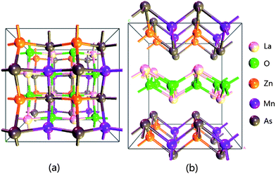 | ||
| Fig. 1 The (a) top view and (b) side view of the La(Mn0.5Zn0.5)AsO crystal. | ||
The electronic structure calculation indicates that the La(Mn0.5Zn0.5)AsO alloy prefers AFM magnetic coupling at its ground state. The FM state is less favorable than the AFM state with an energy difference of about 0.62 eV per supercell. The spin charge density distributions of both AFM and FM states are plotted in Fig. 2a. It is clear that the magnetic moment of La(Mn0.5Zn0.5)AsO is mainly located on Mn atoms. The local magnetic moment of the Mn atom is about 4.19 μB, implying that Mn possesses about +2 e charge with a high spin state. The magnetic coupling between two neighboring [(Mn,Zn)As]− layers was not examined as the interlayer distance between them is about 9.1 Å. Thus, the interlayer magnetic coupling is very weak and was set to be ferromagnetic based on the previous experiments.17,28 The total density of states (DOS) of the La(Mn0.5Zn0.5)AsO alloy are plotted in Fig. 2 for both AFM and FM states. Clearly, the AFM La(Mn0.5Zn0.5)AsO alloy is an intrinsic semiconductor with a band gap of about 1.28 eV (Fig. 2b), while its FM state exhibits a distinct band structure character of an ideal bipolar magnetic semiconductor,8i.e. the valence band and the conduction band approach the Fermi level with opposite spin polarization (Fig. 2c). Therefore, it provides a possibility to tune the spin-polarization direction with an electric field in the La(Mn0.5Zn0.5)AsO alloy at its FM state.
![(a) The distribution of spin charge density in the [(Mn,Zn)As]− layer at FM (upper part) and AFM (lower part) states. The isosurface value is 0.08 e Å−3. Red and blue indicate the positive (spin up) and negative (spin down) values, respectively. The calculated total DOS for La(Mn0.5Zn0.5)AsO at the (b) ground AFM state and (c) FM state. The Fermi level is set to zero.](/image/article/2013/TC/c3tc31514b/c3tc31514b-f2.gif) | ||
| Fig. 2 (a) The distribution of spin charge density in the [(Mn,Zn)As]− layer at FM (upper part) and AFM (lower part) states. The isosurface value is 0.08 e Å−3. Red and blue indicate the positive (spin up) and negative (spin down) values, respectively. The calculated total DOS for La(Mn0.5Zn0.5)AsO at the (b) ground AFM state and (c) FM state. The Fermi level is set to zero. | ||
It is well known that the AFM–FM transition can be realized by various chemical and physical methods in many materials, such as strain29 and carrier doping.30–33 Here, we found that the La(Mn0.5Zn0.5)AsO alloy doped with a small amount of carriers retains its AFM ground state. The magnitude of the energy difference between the AFM and FM states, however, decreases with the increasing doping concentration (the yellow region in Fig. 3a). Meanwhile, the carrier doping induces a semiconductor–metal transition, confirmed with the calculated DOS in Fig. 3b and c. These results are not surprising since the profile of the total DOS does not change much and the Fermi level just moves into either the conduction or valence band when introducing a small amount of electrons or holes in the system.
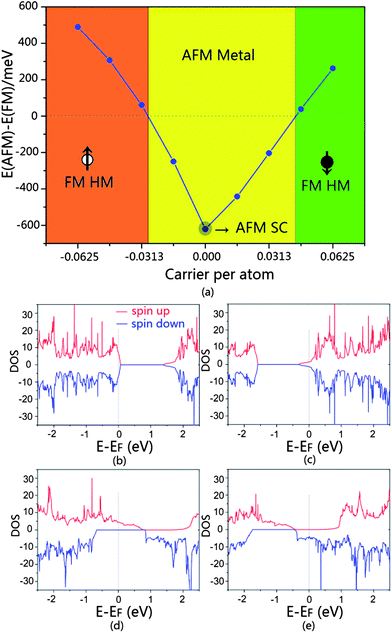 | ||
| Fig. 3 (a) The energy differences per supercell between AFM and FM states are plotted versus the concentration of doped carriers. The positive and negative values are for electron and hole doping, respectively. The up and down arrows indicate spin up and spin down, respectively. Half metal and semiconductor are denoted as HM and SC, respectively. The total DOS of La(Mn0.5Zn0.5)AsO with the doping concentration of (b) 0.0156 holes per atom, (c) 0.0156 electrons per atom, (d) 0.0625 holes per atom and (e) 0.0625 electrons per atom. The Fermi levels are all set to zero. | ||
Continually increasing the doping concentration induces a AFM–FM transition in the La(Mn0.5Zn0.5)AsO alloy, as shown in Fig. 3a. This kind of transition has been observed experimentally in a doped LaMnAsO material.34 Moreover, it can be concluded that the hole doping is more efficient than the electron doping to induce this transition, where the former has a lower concentration at the transition point than the latter. Since the valence and conduction bands near the Fermi level in FM La(Mn0.5Zn0.5)AsO are inversely spin polarized, introducing considerable electrons or holes in FM La(Mn0.5Zn0.5)AsO definitely turns it into a half-metallic material. In particular, the half-metallic La(Mn0.5Zn0.5)AsO alloy shows inverse spin-polarization, depending on the doped carrier type. For instance, the hole-doped La(Mn0.5Zn0.5)AsO alloy would be fully spin-up polarized, while the electron-doped one is spin-down polarized, as shown in Fig. 3d and e. This behavior presents a potential to alter the spin-polarization direction in La(Mn0.5Zn0.5)AsO by carrier doping, which can be realized in experiment just by altering the sign of applied gate voltage. Note that the spin-unrestricted DFT method may predict artificial magnetism in finite carbon systems, such as nanographene fragments, for the so-called “singlet open-shell state” problem. Using some advanced multideterminant methods, such as multi-configurational self-consistent field method or coupled-cluster method, or taking account of the possible singlet–triplet mixture interpolated from more sophisticated methods than UDFT, the relative spin correlation can be well treated.35,36 In this paper, however, the system we studied is a three-dimensional crystal material containing transition metals, where the UDFT method has been widely used to predict reliable magnetism in massive similar systems.
In essence, the electrical control of spin in the La(Mn0.5Zn0.5)AsO alloy is similar to the previously proposed bipolar magnetic semiconductors, where the spin direction of carriers is manipulated by moving the Fermi level to either the conduction band or the valence band under an electric field.8 The only difference is that the bipolar spin polarization in the La(Mn0.5Zn0.5)AsO alloy is obtained via carrier-doping induced AFM–FM phase transition. As shown in Fig. 3d and e, the La(Mn0.5Zn0.5)AsO alloy shows a nearly vanished spin-flip gap between valence band and conduction band edges, and the big spin-conserved gaps are about 0.83 and 1.49 eV for spin-up and spin-down channels, respectively. Thus, the spin-polarization direction can be switched easily by a small shift of the Fermi level and the applied gate voltage can be tuned in a wide range while maintaining half-metallic conduction.
To understand the profound AFM–FM transition in the La(Mn0.5Zn0.5)AsO alloy, we plotted both the site- and orbital-projected DOS at the doping concentration of 0.0625 carriers per atom in Fig. 4. In its neutral state, i.e. without doping, the strong superexchange interaction37 mediated by nonmagnetic As atoms leads to the AFM coupling between adjacent Mn atoms. With high hole-doping concentration, La(Mn0.5Zn0.5)AsO exhibits a robust FM order and the states around the Fermi level are mainly contributed by As 4p and Mn 3d orbitals (Fig. 4a and c). The strong hybridization between them suggests that the ferromagnetism in the doped La(Mn0.5Zn0.5)AsO alloy originates from Zener's p–d exchange interaction.38,39 Usually, Zener's p–d exchange interaction leads to a higher Curie temperature with a higher doping concentration, consistent with the predicted increase of energy difference between AFM and FM states in the La(Mn0.5Zn0.5)AsO alloy (Fig. 3a). Therefore, the magnetic order transition in the La(Mn0.5Zn0.5)AsO alloy is a competition result between the superexchange and Zener's p–d exchange interactions. For electron doping, however, the hybridization between As 4p and Mn 3d orbitals is weak (Fig. 4b and d), which partly explains why the electron doping is less efficient than hole doping for this transition in the La(Mn0.5Zn0.5)AsO alloy.
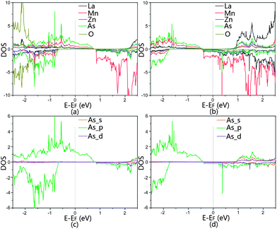 | ||
| Fig. 4 (a) and (b) are the site-projected DOS of La(Mn0.5Zn0.5)AsO with the doping concentration of 0.0625 holes per atom and 0.0625 electrons per atom, respectively. (c) and (d) are the orbital-projected DOS for As atoms at the same doping concentration. The Fermi energy levels are set to zero. | ||
Conclusions
In conclusion, we presented a new spintronic material La(Mn0.5Zn0.5)AsO alloy obtained from two experimentally synthesized rare earth element transition metal arsenide oxides LaMnAsO and LaZnAsO. The carrier doping induces a transition from AFM semiconductor to FM half metal in it. In particular, the spin-polarization direction in La(Mn0.5Zn0.5)AsO is switchable, depending on the type of doped carriers. The La(Mn0.5Zn0.5)AsO alloy serves as an example of a new type of spintronic materials which can provide completely spin-polarized currents with a tunable spin-polarization direction by applying an external gate voltage. It is expected that the various analogous ZrCuSiAs-type compounds will form a promising family of precursors for exploring similar materials to enable the electrical control of spin. Very recently, a two dimensional “1111” diluted magnetic semiconducting (La1−xBax)(Zn1−xMnx)AsO in bulk form has been synthesized,40 implying the great potential of this type of material in spintronic applications.Acknowledgements
This work is partially supported by the National Key Basic Research Program (2011CB921404 and 2012CB922001), by NSFC (21121003, 91021004, 20933006, 11004180, and 51172223), by the Strategic Priority Research Program of CAS (XDB01020300), and by USTCSCC, SCCAS, Tianjin, and Shanghai Supercomputer Centers.Notes and references
- S. A. Wolf, D. D. Awschalom, R. A. Buhrman, J. M. Daughton, S. von Molnar, M. L. Roukes, A. Y. Chtchelkanova and D. M. Treger, Science, 2001, 294, 1488 CrossRef CAS PubMed.
- H. Ohno, A. Shen, F. Matsukura, A. Oiwa, A. Endo, S. Katsumoto and Y. Iye, Appl. Phys. Lett., 1996, 69, 363 CrossRef CAS.
- R. A. de Groot, F. M. Mueller, P. G. van Engen and K. H. J. Buschow, Phys. Rev. Lett., 1983, 50, 2024 CrossRef CAS.
- X. L. Wang, Phys. Rev. Lett., 2008, 100, 156404 CrossRef CAS.
- B. A. Bernevig, T. L. Hughes and S. C. Zhang, Science, 2006, 314, 1757 CrossRef CAS PubMed.
- Y. Kato, R. C. Myers, D. C. Driscoll, A. C. Gossard, J. Levy and D. D. Awschalom, Science, 2003, 299, 1201 CrossRef CAS PubMed.
- K. C. Nowack, H. F. L. Koppens and Y. V. Nazarov, Science, 2007, 318, 1430 CrossRef CAS PubMed.
- X. X. Li, X. J. Wu, Z. Y. Li, J. L. Yang and J. G. Hou, Nanoscale, 2012, 4, 5680 RSC.
- L. Yuan, Z. Y. Li and J. L. Yang, Phys. Chem. Chem. Phys., 2013, 15, 497 RSC.
- V. V. Bannikov and A. L. Ivanovskii, JETP Lett., 2013, 96, 735 CrossRef CAS.
- Y. Ding and Y. Wang, Appl. Phys. Lett., 2013, 102, 143115 CrossRef.
- Y. Kamihara, T. Watanabe, M. Hirano and H. Hosono, J. Am. Chem. Soc., 2008, 130, 3296 CrossRef CAS PubMed.
- H. Yanagi, R. Kawamura, T. Kamiya, Y. Kamihara, M. Hirano, T. Nakamura, H. Osawa and H. Hosono, Phys. Rev. B: Condens. Matter Mater. Phys., 2008, 77, 224431 CrossRef.
- K. Ueda, S. Inoue, S. Hirose, H. Kawazoe and H. Hosono, Appl. Phys. Lett., 2000, 77, 2701 CrossRef CAS.
- A. T. Nientiedt, W. Jeitschko, P. G. Pollmeier and M. Brylak, Z. Naturforsch., B: J. Chem. Sci., 1997, 52, 560 CAS.
- A. Y. Nientiedt and W. Jeitschko, Inorg. Chem., 1998, 37, 386 CrossRef CAS PubMed.
- N. Emery, E. J. Wildman, J. M. S. Skakle, G. Giriat, R. L. Smith and A. C. Mclaughlin, Chem. Commun., 2010, 46, 6777 RSC.
- K. Kayanuma, R. Kawamura, H. Hiramatsu, H. Yanagi, M. Hirano, T. Kamiya and H. Hosono, Thin Solid Films, 2008, 516, 5800 CrossRef CAS PubMed.
- J. P. Perdew, K. Burke and M. Ernzerhof, Phys. Rev. Lett., 1996, 77, 3865 CrossRef CAS.
- G. Kresse and J. Furthmüller, Phys. Rev. B: Condens. Matter Mater. Phys., 1996, 54, 11169 CrossRef CAS.
- A. I. Liechtenstein, V. I. Anisimov and J. Zaane, Phys. Rev. B: Condens. Matter Mater. Phys., 1995, 52, 5467 CrossRef.
- J. Okabayashi, A. Kimura, O. Rader, T. Mizokawa, A. Fujimori, T. Hayashi and M. Tanaka, Phys. Rev. B: Condens. Matter Mater. Phys., 1998, 58, 4211 CrossRef.
- K. Sato, P. H. Dederichs, H. Katayama-Yoshida and J. Kudrnovský, J. Phys.: Condens. Matter, 2004, 16, 5491 CrossRef.
- M. Wierzbowska, D. Sánchez-Portal and S. Sanvito, Phys. Rev. B: Condens. Matter Mater. Phys., 2004, 70, 235209 CrossRef.
- P. Larson, W. R. L. Lambrecht, A. Chantis and M. Schilfgaarde, Phys. Rev. B: Condens. Matter Mater. Phys., 2007, 75, 045114 CrossRef.
- P. E. Blöchl, Phys. Rev. B: Condens. Matter Mater. Phys., 1994, 50, 17953 CrossRef.
- R. Pöttgena and D. Johrendt, Z. Naturforsch., B: J. Chem. Sci., 2008, 63, 1135 Search PubMed.
- H. Yanagi, T. Watanabe, K. Kodama, S. Iikubo, S. Shamoto, T. Kamiya, M. Hirano and H. Hosono, J. Appl. Phys., 2009, 105, 093916 CrossRef.
- J. S. White, M. Bator, Y. Hu, H. Luetkens, J. Stahn, S. Capelli, S. Das, M. Döbeli, Th. Lippert, V. K. Malik, J. Martynczuk, A. Wokaun, M. Kenzelmann, Ch. Niedermayer and C. W. Schneider, Phys. Rev. Lett., 2013, 111, 037201 CrossRef CAS.
- T. Story, R. R. Gał
![[a with combining cedilla]](https://www.rsc.org/images/entities/char_0061_0327.gif) zka, R. B. Frankel and P. A. Wolff, Phys. Rev. Lett., 1986, 56, 777 CrossRef CAS.
zka, R. B. Frankel and P. A. Wolff, Phys. Rev. Lett., 1986, 56, 777 CrossRef CAS. - K. R. Kittilstved, D. A. Schwartz, A. C. Tuan, S. M. Heald, S. A. Chambers and D. R. Gamelin, Phys. Rev. Lett., 2006, 97, 037203 CrossRef.
- J. Philip, A. Punnoose, B. I. Kim, K. M. Reddy, S. Layne, J. O. Holmes, B. Satpati, P. R. LeClair, T. S. Santos and J. S. Moodera, Nat. Mater., 2006, 5, 298 CrossRef CAS PubMed.
- K. Zhao, Z. Deng, X. C. Wang, W. Han, J. L. Zhu, X. Li, Q. Q. Liu, R. C. Yu, T. Goko, B. Frandsen, L. Liu, F. Ning, Y. J. Uemura, H. Dabkowska, G. M. Luke, H. Luetkens, E. Morenzoni, S. R. Dunsiger, A. Senyshyn, P. Böni and C. Q. Jin, Nat. Commun., 2013, 4, 1442 CrossRef CAS PubMed.
- T. Hanna, S. Matsuishi, K. Kodama, T. Otomo, S. Shamoto and H. Hosono, Phys. Rev. B: Condens. Matter Mater. Phys., 2013, 87, 020401(R) Search PubMed.
- S. Perumal, B. Minaev and H. Ågren, J. Chem. Phys., 2012, 136, 104702 CrossRef CAS PubMed.
- M. S. Deleuze, M. Huzak and B. Hajgató, J. Mol. Model., 2013, 19, 2699 CrossRef CAS PubMed.
- P. W. Anderson, Phys. Rev., 1959, 115, 2 CrossRef CAS.
- T. Dietl, H. Ohno, F. Matsukura, J. Cibert and D. Ferrand, Science, 2000, 287, 1019 CrossRef CAS.
- T. Jungwirth, J. König, J. Sinova, J. Kučera and A. H. MacDonald, Phys. Rev. B: Condens. Matter Mater. Phys., 2002, 66, 012402 CrossRef.
- C. Ding, H. Man, C. Qin, J. Lu, Y. Sun, Q. Wang, B. Yu, C. Feng, T. Goko, C. J. Arguello, L. Liu, B. J. Frandsen, Y. J. Uemura, H. Wang, H. Luetkens, E. Morenzoni, W. Han, C. Q. Jin, T. Munsie, T. J. Williams, R. M. D'Ortenzio, T. Medina, G. M. Luke, T. Imai and F. L. Ning, Phys. Rev. B: Condens. Matter Mater. Phys., 2013, 88, 041102(R) Search PubMed.
| This journal is © The Royal Society of Chemistry 2013 |