 Open Access Article
 This Open Access Article is licensed under a
 Creative Commons Attribution 3.0 Unported Licence
Photoinduced electron and hole transfer in CdS:P3HT nanocomposite films: effect of nanomorphology on charge separation yield and solar cell performance†
Simon A. Dowland, Luke X. Reynolds, Andrew MacLachlan, Ute B. Cappel and Saif A. Haque*
Department of Chemistry, Imperial College London, South Kensington Campus, Exhibition Road, SW7 2AY, UK. E-mail: s.a.haque@imperial.ac.uk
First published on 10th October 2013
Abstract
The influence of morphology on the photophysical properties of blend films containing in situ grown CdS and poly(3-hexylthiophene-2,5-diyl) (P3HT), fabricated utilising a metal xanthate single source precursor, is reported. A combination of transient absorption spectroscopy (TAS), transmission electron microscopy (TEM) and photovoltaic device measurements are employed to study the relationship between the efficiency of charge separation, photocurrent generation and thin film morphology. We identify that a significant proportion of the extractable charge originates from the direct excitation of CdS followed by hole-transfer to the P3HT polymer. The yield of this hole-transfer step from the inorganic CdS to the organic polymer is largely unaffected by the film's nanomorphology, while the dissociation of P3HT excitons into free charges at the CdS:P3HT interface is found to be strongly dependent on this parameter with high yields of charge transfer only being achieved at high CdS loadings. The present study elucidates design rules for the optimization of hybrid inorganic–organic solar energy conversion devices.
Introduction
Interest in the development of hybrid solar cells has been growing in recent years, due to a desire to develop flexible, solution-processable, cost-effective devices that incorporate the attractive properties commonly associated with both inorganic and organic semiconductor materials.1–3 Work on hybrid solar cells, to date, has utilised a variety of inorganic materials in conjunction with organic semiconductors, within the active layer, such as CdS, PbS, CdSe, CuInS2, and ZnO.3–7Fig. 1 shows the main electronic processes occurring in a hybrid solar cell. The efficient operation of such hybrid solar cells critically depends on the ability to achieve a high yield of photoinduced charge generation at the inorganic–organic heterojunction. One limitation to achieving these high yields has been the electron transfer from an excited-state of a donor polymer to an inorganic electron acceptor material (Process 2). The excited state in organic semiconductors is well known to be strongly bound and suffer from short diffusion lengths which dictate the ideal nanostructures that will facilitate efficient charge photogeneration and device performance.8 It is commonly considered that the charge generation yield in hybrids can be mitigated through altering nanomorphology of the photoactive layer such that excited states are generated within a distance of the charge separating interface shorter than the diffusion length of that excited state. In addition, recent research has shown that interfacial energetics and local crystallinity can play a key role in determining the efficiency of long-range charge pair generation at hybrid inorganic–polymer heterojunctions.9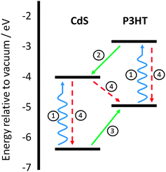 | ||
| Fig. 1 Energy level diagram of a CdS:P3HT blend showing the main electronic processes occurring in a hybrid solar cell. (1) Absorption within both components of the layer. (2) Electron transfer from the organic donor to the inorganic acceptor. (3) Hole transfer from the inorganic acceptor to the organic donor. (4) Geminate and non-geminate recombination processes leading to excited state decay. | ||
Optimal incorporation of inorganic structures into solution processed polymer solar cells will inevitably involve their use as light absorbers along with the organic component in order to maximise the absorbing potential of the film. Here, charge separation can be achieved by a photo-induced hole-transfer reaction from the inorganic absorber to the polymer semiconductor (Process 3).10 However, in systems where both active layer components may generate free charges the focus has usually been on the behaviour of excited states formed within the organic component. Moreover, it is well known that the behaviour of the excited state in inorganic crystals is governed less by a strong coulombic interaction.11,12 Hence, in a nanostructured blend, the hole transfer process is therefore likely to exhibit different dependence on film morphology to that of the electron transfer from polymer. However, studies addressing the influence of morphology on the relative yields of electron and hole transfer at inorganic–organic heterojunctions remain limited.
In this paper, we present a comprehensive study of the influence of composition ratio and morphology of in situ grown CdS:P3HT blends on the photophysical properties of films and devices. We have studied the charge generation for the different blend ratios at different wavelengths by both photoluminescence (PL) and transient absorption spectroscopy (TAS), such that we can distinguish charges generated from excitation of the organic and inorganic component. Charge yields from each component show a different dependence on composition and morphology. We show that the yield of electron transfer (Process 2, Fig. 1) is strongly dependent on film morphology whereas the yield of hole-transfer (Process 3, Fig. 1) is largely unaffected by the film nanomorphology. Finally we show that an increase in total charge generation does not always correlate with superior device performance and that effective device performance can be hindered by poor charge extraction when the polymer concentration is low. The present findings are discussed with relevance to the design and optimization of hybrid inorganic–organic solar cells.
Results and discussion
Active layers with different ratios of P3HT and CdS were prepared on glass substrates using a precursor-based fabrication route as previously reported.13,14 CdS:P3HT nanocomposite films were prepared by spin coating a chlorobenzene solution containing varying ratios of Cd(S2COC2H5)2(C5H5N)2 and P3HT. The resultant films were annealed at 160 °C to generate the CdS:P3HT films. Fig. 2 shows the steady state absorption spectra of the CdS:P3HT films studied herein. The contribution to the absorption from CdS can be seen below 500 nm with a shoulder at approximately 460 nm and a further rise in absorption at shorter wavelengths. Characteristic P3HT absorption peaks are visible at 520 nm and 555 nm along with a further P3HT absorption peak at 607 nm which has been attributed to the π–π* transition as a result of π-stacking within more ordered regions of the polymer film.15 It is apparent from the data presented in Fig. 2 and S1† that increasing CdS content within the film, results in a reduction in the crystallinity of the P3HT within the films.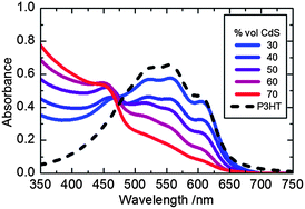 | ||
| Fig. 2 Absorbance profiles of CdS:P3HT blends (from blue to red line, 30% to 70% by volume CdS respectively) and pure P3HT film (black dashed line). | ||
Transmission electron microscopy measurements were conducted to determine the morphology of the CdS:P3HT nanocomposite films. Fig. 3 shows the corresponding bright field transmission electron microscopy (TEM) images for samples prepared at 30%, 50% and 70% volume CdS (Fig. 3a–c, respectively). The samples display distinct morphologies with dark regions attributed to increased CdS content and lighter regions to P3HT. The CdS adopts a wurtzite hexagonal phase as shown by XRD.9 At 30% CdS, significant regions of phase segregated P3HT can be seen while the CdS appears to be relatively dispersed. We note that the phase separation observed is lateral not vertical, but distinguishing this difference is beyond the scope of this paper; we have assumed they are similar. Increasing the CdS content has the effect of reducing the length scale of phase separation thereby leading to a finer mixing of the two components as has been suggested before.14,16 PL quenching measurements were performed on samples analogous to those presented in Fig. 2. Increased quenching of P3HT excitons was observed with increasing CdS volume fractions (Fig. S2†). This behaviour is most likely due to a greater fraction of photogenerated excitons being formed in the vicinity (within the exciton diffusion length) of the CdS:P3HT heterojunction where charge separation can occur. Furthermore, this observation is in agreement with the TEM data shown in Fig. 3, which indicates smaller P3HT domains as the CdS volume fraction is increased.
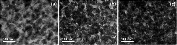 | ||
| Fig. 3 Bright field transmission electron microscopy images of CdS:P3HT blends taken at 30% CdS (a), 50% CdS (b) and 70% CdS (c) volume fractions. | ||
We now consider the influence of film morphology on the efficiency of charge separation. For this purpose, laser-based microsecond–millisecond transient absorption spectroscopy was used as described elsewhere in the literature.17 In this study an excitation wavelength of 355 nm was used to generate electron–hole pairs primarily in the CdS and 550 nm was used to generate excitons solely in the P3HT. Pulsed laser excitation at either 355 nm or 550 nm resulted in the appearance of a broad transient absorption band centred at 950–1000 nm. We attribute this transient absorption band to the hole-polaron in the P3HT.18 The charge recombination kinetics were determined by monitoring the decay of the transient absorption band at 980 nm back to ground state (see Fig. S3†). The amplitude of the transient absorption signals (ΔA) is proportional to the concentration of photogenerated P3HT hole polarons. Fig. 4 shows a plot of the magnitude of the 980 nm signal at 1 μs following excitation at 355 nm and 550 nm for samples containing different CdS volume fractions. Averages were taken of the change in absorbance from 0.9 μs to 1.1 μs corrected for the number of incident pump photons and the light harvesting efficiency of the films. At 1 μs the magnitude of the signal becomes an assay for the number of long-lived charges generated, and is therefore a useful measure of the yield of charge separation.18 It is apparent from the data shown in Fig. 4, that the yield of photogenerated P3HT polarons is largely unaffected by film nanomorphology upon sample excitation at 355 nm. In contrast, the yield of photogenerated P3HT polarons displays a strong dependence on morphology following excitation at 550 nm.
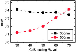 | ||
| Fig. 4 Change in optical density averaged over 0.9 μs to 1.1 μs taken from transient absorption spectroscopy (TAS) kinetics measurements corrected for incident photons on sample and light harvesting efficiency. Samples pumped at 355 nm and 550 nm, and probed at 980 nm. | ||
The next question that arises relates to the origin of the observations presented in Fig. 4. We consider first the charge generation process following optical excitation (at 550 nm) of the P3HT component. The current observations can be rationalised by considering the behaviour of the excited states within the polymer. The diffusion length constraints of excitons generated within organic semiconductors are well known and consequently there is a need for tight control of the nanostructure in order to facilitate a high yield of exciton dissociation and charge generation.8 As the CdS loading is increased the P3HT domain size is reduced making the migration of excitons, formed within P3HT, more likely to reach an interface and subsequently increase the charge generation yield. It is noteworthy that a greater CdS content may result in a more crystalline character and a higher degree of interconnectivity within the CdS domains, both of which have been shown to lead to a more facile electron transfer process.9,16
In contrast, charge generation following excitation of CdS at 355 nm shows little or no dependence on the morphology. Electron–hole pairs formed within inorganic materials, like CdS, are typically subject to a weaker coulomb attraction, possibly leading to generation of free charge carriers within the inorganic nanocrystal phase.19 It is feasible that after free charge carrier formation, the holes migrate to the inorganic–organic heterojunction to undergo a transfer process to the polymer. Moreover, the remarkably weak dependence of the charge generation yield (following 355 nm excitation) upon film morphology implies that the diffusion length of the photogenerated CdS holes must be greater than the CdS domain size across all compositions studied herein. Such a picture is supported by reported hole mobilities in single crystal CdS as high as 15 cm2 V−1 s−1 at room temperature.20 This is significantly higher than has been reported in P3HT and suggests that the movement of photogenerated holes in CdS is relatively unhindered.21 More detailed studies addressing the mechanisms of charge generation within these systems are underway and will be reported on in due course.
We now consider the relationship between charge generation yield and photocurrent extraction as a function of film nanomorphology. More specifically, we compare the overall TAS yields with the short circuit currents (JSC's) of the corresponding devices (Fig. 5). TAS yields at excitation wavelengths, λ, between 355 nm and 600 nm (ΔA(λ)), obtained by averaging TAS kinetics between 0.9 μs and 1.1 μs and correcting for the incident photon flux (Fig. S4†), were used to calculate the relative approximate charge generation yield under AM 1.5 illumination (Φrel) for each sample as described in eqn (1),
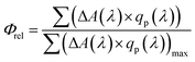 | (1) |
 | ||
| Fig. 5 Relative charge generation of samples corrected for the solar spectrum and normalised for varying compositions of CdS:P3HT (red circles). Short circuit currents of devices fabricated with corresponding compositions of the active layer (black squares). | ||
 | ||
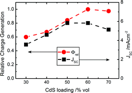
| Fig. 6 J–V curves for devices fabricated utilising active layers with varied compositions of CdS:P3HT. Displayed are devices fabricated with 30 vol% CdS (blue diamonds), 50 vol% CdS (purple squares), and 70 vol% CdS (red triangles). | ||
| Device | Composition (vol% Cds) | VOC (V) | JSC (mA cm−2) | FF | PCE (%) |
|---|---|---|---|---|---|
| ◊ | 30 | 0.75 | 3.57 | 0.53 | 1.41 |
| 40 | 0.76 | 4.60 | 0.50 | 1.77 | |
| □ | 50 | 0.78 | 5.83 | 0.46 | 2.10 |
| 60 | 0.78 | 5.83 | 0.43 | 1.93 | |
| Δ | 70 | 0.80 | 5.14 | 0.42 | 1.74 |
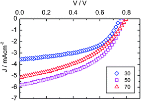
Turning our attention to the 50% CdS:P3HT blend, we compare the light harvesting efficiency (LHE), charge generation and charge extraction properties at different wavelengths (Fig. 7a). It can be seen that the TAS yields are well matched with the incident photon to electron conversion efficiency (IPCE) of the device suggesting that charge extraction is not dependent on excitation wavelength. We attribute the decrease in IPCE spectrum observed below 400 nm to a filtering of the incident light by layers only present in devices (ITO, TiO2 layer and CdS seed layer, see Experimental section). On the other hand, both IPCE and charge yields show relative decrease compared to the light harvesting efficiency in regions where predominantly P3HT absorbs, confirming once more the less than optimal charge generation from P3HT excitons. Integrating the IPCE spectrum and using the simple assumption that absorption above and below 480 nm is solely carried out by the P3HT and CdS respectively (Fig. 7b), the relative contribution to the current in a device from electron and hole transfer, respectively, can be estimated. Charges generated from excitation of CdS account for approximately 60% of the integrated IPCE and for close to 50% of the JSC under AM 1.5 illumination. This is a significant contribution to the overall photocurrent, especially considering the lower photon flux at wavelengths below 480 nm than at longer wavelengths. We note that this 480 nm cut-off is not strictly accurate, but it is a valid simplification that highlights the differences between the organic and inorganic components. A route to achieving higher photocurrents in hybrid solar cells might therefore be to use inorganic absorbers with smaller band gaps to make better use of the efficient hole transfer process.
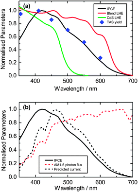 | ||
| Fig. 7 (a) Light harvesting efficiencies of CdS (green line) and 50 vol% CdS:P3HT blend (red line). IPCE of 50 vol% CdS device (black line) and TAS change in optical density averaged over 0.9 μs to 1.1 μs of 50 vol% CdS:P3HT film (blue squares). (b) Estimated IPCE contribution for CdS and P3HT (black line) and expected contribution to the current under light exposure (black dotted line) based on AM 1.5 solar spectrum (red dotted line). | ||
In summary we have reported on the relationship between nanomorphology and photophysical properties of in situ grown CdS:P3HT blends. Specifically, we have demonstrated that nanomorphology may be controlled by altering the relative amounts of the active layer components. Through transient absorption studies we have shown that charge generation from P3HT excitons is heavily nanomorphology dependent while charge generation through hole transfer from CdS is largely unaffected by the morphology of the film. The electron transfer process benefits from small P3HT domain sizes while photocurrent extraction required for good photovoltaic devices relies on larger and/or more crystalline P3HT domains. Furthermore, charge generation from a hole transfer process appears to be a substantial contributor to the device current. Therefore, these findings demonstrate a viable route to improve the efficiency of hybrid solar cells through an extension of the absorption spectrum of the inorganic component.
Experimental
Spectroscopic characterization
Steady state UV/vis absorption measurements were made with a Perkin-Elmer Lambda 25 Spectrophotometer. Photoluminescence measurements were made with a Horiba Jobin Yvon Fluorolog-2.Sample morphology was studied by transmission electron microscopy (TEM) using a JEOL 2000 MkII electron microscope operated at 200 kV. Films for TEM were fabricated on PEDOT:PSS (Ossila, AI 4083) itself spin coated onto glass to act as a water soluble sacrificial substrate. Free floating films were then transferred to copper grids for imaging in a ‘top-down’ fashion.
Transient absorption kinetics were measured by exciting the sample film, under a dynamic nitrogen atmosphere, with an Nd:YAG laser or the output from an optical parametric oscillator (Oppolette) pumped by the Nd:YAG laser. The time duration of the pump-pulses was 20 ns. The excitation wavelengths used ranged from 355 nm to 600 nm, at intensities of ∼5–20 μJ cm−2 and a repetition frequency of 20 Hz. A 100 W quartz halogen lamp (Bentham, IL 1) with a stabilized power supply (Bentham, 605) was used as a probe light source, with a probe wavelength of 980 nm used. The probe light passing through the sample film was detected with a silicon photodiode (Hamamatsu Photonics, S1722-01). The signal from the photodiode was amplified before being passed through electronic band-pass filters (Costronics Electronics). The amplified signal was collected with a digital oscilloscope (Tektronics, TDS220), which was synchronized with a trigger signal from the pump laser pulse from a photodiode (Thorlabs Inc., DET210). To reduce stray light, scattered light, and sample emission, two monochromators and appropriate optical cutoff filters were placed before and after the sample.
Device fabrication
Devices fabricated all utilised an inverted architecture with the following layers; ITO/TiO2/CdS/active layer (CdS:P3HT)/PEDOT:PSS/Ag. Cadmium xanthate precursor was prepared as described elsewhere.13 ITO sputtered substrates (Psiotec Ltd) were sonicated in, acetone, detergent, deionised water, and isopropanol. A solution of titanium isopropoxide (97%, Sigma Aldrich) and ethanolamine in 2-methoxyethanol was spun on substrates, which were then heated to 450 °C. A solution of the CdS precursor dissolved in chlorobenzene was deposited over the TiO2 layer by spin coating and annealed under N2 at 160 °C for 30 min in order to form the CdS layer. Chlorobenzene solutions of the CdS precursor and P3HT were mixed in varying proportions to facilitate the different volume ratios. These were then spun over the CdS layer followed by annealing at 160 °C for 1 h. PEDOT:PSS (Ossila, AI 4083) was spun onto this layer before deposition of 150 nm Ag top electrode in vacuum.Device characterisation
Current–voltage characteristics of the cells were measured using a 150 W xenon lamp (ScienceTech SS150Wsolar simulator) equipped with an IR filter (Water Filter) and AM 1.5 filter (ScienceTech). EQE measurements were conducted using irradiation from a quartz halogen lamp (Bentham IL1) filtered through an autonomous monochromator (Bentham M300). Current measurements were also conducted using a Keithley 2400 series source meter.Acknowledgements
We acknowledge financial support from the Engineering and Physical Science Research Council (EPSRC) through the UK-India (EP/H040218/2) and SuperGen (EP/GO31088/1) programmes. SAH acknowledges support from the Royal Society through award of a University Research Fellowship. We acknowledge support from the European Union through award of a Marie Curie Intra-European Fellowship.References
- M. Wright and A. Uddin, Sol. Energy Mater. Sol. Cells, 2012, 107, 87–111 CrossRef CAS PubMed.
- F. Gao, S. Ren and J. Wang, Energy Environ. Sci., 2013, 6, 2020–2040 CAS.
- A. H. Ip, S. M. Thon, S. Hoogland, O. Voznyy, D. Zhitomirsky, R. Debnath, L. Levina, L. R. Rollny, G. H. Carey, A. Fischer, K. W. Kemp, I. J. Kramer, Z. Ning, A. J. Labelle, K. W. Chou, A. Amassian and E. H. Sargent, Nat. Nanotechnol., 2012, 7, 577–582 CrossRef CAS PubMed.
- S. Ren, L.-Y. Chang, S.-K. Lim, J. Zhao, M. Smith, N. Zhao, V. Bulović, M. Bawendi and S. Gradečak, Nano Lett., 2011, 11, 3998–4002 CrossRef CAS PubMed.
- S. D. Oosterhout, L. J. A. Koster, S. S. van Bavel, J. Loos, O. Stenzel, R. Thiedmann, V. Schmidt, B. Campo, T. J. Cleij, L. Lutzen, D. Vanderzande, M. M. Wienk and R. A. J. Janssen, Adv. Energy Mater., 2011, 1, 90–96 CrossRef CAS.
- S. Dayal, N. Kopidakis, D. C. Olson, D. S. Ginley and G. Rumbles, Nano Lett., 2009, 10, 239–242 CrossRef PubMed.
- T. Rath, M. Edler, W. Haas, A. Fischereder, S. Moscher, A. Schenk, R. Trattnig, M. Sezen, G. Mauthner, A. Pein, D. Meischler, K. Bartl, R. Saf, N. Bansal, S. A. Haque, F. Hofer, E. J. W. List and G. Trimmel, Adv. Energy Mater., 2011, 1, 1046–1050 CrossRef CAS.
- J. E. Kroeze, T. J. Savenije, M. J. W. Vermeulen and J. M. Warman, J. Phys. Chem. B, 2003, 107, 7696–7705 CrossRef CAS.
- N. Bansal, L. X. Reynolds, A. MacLachlan, T. Lutz, R. S. Ashraf, W. Zhang, C. B. Nielsen, I. McCulloch, D. G. Rebois, T. Kirchartz, M. S. Hill, K. C. Molloy, J. Nelson and S. A. Haque, Sci. Rep., 2013, 3, 1531 CrossRef CAS PubMed.
- F. T. F. O'Mahony, T. Lutz, N. Guijarro, R. Gomez and S. A. Haque, Energy Environ. Sci., 2012, 5, 9760–9764 CAS.
- G. H. Wannier, Phys. Rev., 1937, 52, 191–197 CrossRef CAS.
- N. Chestnoy, T. D. Harris, R. Hull and L. E. Brus, J. Phys. Chem., 1986, 90, 3393–3399 CrossRef CAS.
- H. C. Leventis, S. P. King, A. Sudlow, M. S. Hill, K. C. Molloy and S. A. Haque, Nano Lett., 2010, 10, 1253–1258 CrossRef CAS PubMed.
- S. Dowland, T. Lutz, A. Ward, S. P. King, A. Sudlow, M. S. Hill, K. C. Molloy and S. A. Haque, Adv. Mater., 2011, 23, 2739–2744 CrossRef CAS PubMed.
- F. C. Spano, J. Clark, C. Silva and R. H. Friend, J. Chem. Phys., 2009, 130, 074904–074916 CrossRef PubMed.
- L. X. Reynolds, T. Lutz, S. Dowland, A. MacLachlan, S. King and S. A. Haque, Nanoscale, 2012, 4, 1561–1564 RSC.
- D. Credgington, F. C. Jamieson, B. Walker, T.-Q. Nguyen and J. R. Durrant, Adv. Mater., 2012, 24, 2135–2141 CrossRef CAS PubMed.
- T. M. Clarke, A. M. Ballantyne, J. Nelson, D. D. C. Bradley and J. R. Durrant, Adv. Funct. Mater., 2008, 18, 4029–4035 CrossRef CAS.
- C.-h. Wu and R. H. Bube, J. Appl. Phys., 1974, 45, 648–660 CrossRef CAS.
- W. E. Spear and J. Mort, Proc. Phys. Soc., 1963, 81, 130 CrossRef CAS.
- H. Sirringhaus, P. J. Brown, R. H. Friend, M. M. Nielsen, K. Bechgaard, B. M. W. Langeveld-Voss, A. J. H. Spiering, R. A. J. Janssen, E. W. Meijer, P. Herwig and D. M. de Leeuw, Nature, 1999, 401, 685–688 CrossRef CAS PubMed.
Footnote |
| † Electronic supplementary information (ESI) available. See DOI: 10.1039/c3ta12962d |
| This journal is © The Royal Society of Chemistry 2013 |