 Open Access Article
Creative Commons Attribution 3.0 Unported Licence
A fast operation of nanometer-scale metallic memristors: highly transparent conductance channels in Ag2S devices†
Attila
Geresdi
,
Miklós
Csontos
*,
Agnes
Gubicza
,
András
Halbritter
and
György
Mihály
Department of Physics, Budapest University of Technology and Economics and Condensed Matter Research Group of the Hungarian Academy of Sciences, Budafoki ut 8, 1111 Budapest, Hungary. E-mail: csontos@dept.phy.bme.hu
First published on 6th December 2013
Abstract
The nonlinear transport properties of nanometer-scale junctions formed between an inert metallic tip and an Ag film covered by a thin Ag2S layer are investigated. Suitably prepared samples exhibit memristive behavior with technologically optimal ON and OFF state resistances yielding to resistive switching on the nanosecond time scale. Utilizing point contact Andreev reflection spectroscopy, we studied the nature of electron transport in the active volume of memristive junctions showing that both the ON and OFF states correspond to truly nanometer-scale, highly transparent metallic channels. Our results demonstrate the merits of Ag2S nanojunctions as nanometer-scale memory cells which can be switched by nanosecond voltage pulses.
The ongoing miniaturization beyond the limitations of current complementary metal-oxide-semiconductor (CMOS) technology is a major challenge in nanoscience.1–3 Using individual atoms or molecules in nanoelectronic circuits has been a breakthrough towards the ultimate single atomic size limit.4,5 The persisting technological difficulties in the reliable assembly of low resistance single molecule devices, however, still represent a major barrier to fast applications preferring low RC time constants with the capacitance of the environment. Alternatively, reversible solid state electrochemical reactions have been proposed to form tunable atomic scale junctions between metallic electrodes. The first results are extremely promising for the short term realization of highly integrated information storage applications.6–13 The resistive state of a memory element, called memristor,6,8,9,14–16 is altered by biasing the device above its writing threshold (Vth). Readout is performed at lower signal levels which preserve the stored information.
Chalcogenide compounds have been put forward in the context of the “atomic switch”,7 consisting of an inert metallic electrode (Me) and an Ag layer capped with the solid state ionic conductor Ag2S. Upon positively biasing the Ag electrode with respect to Me, a metallic Ag propulsion is grown on the Ag2S–Me interface shunting the electrodes thus creating the non-volatile ON state of the device.17–21 Real-time high resolution transmission electron microscopy (HRTEM) imaging22 and first-principles band structure calculations23,24 suggested that a structural phase transition in the Ag2S layer also plays a role in the resistive transition.25
Since the pioneering experiments reported on Ag–Ag2S–Pt devices7 the development of memory cells based on memristive systems has achieved a remarkable progress. Besides providing an interesting model system for neural networks,26–28 Ag2S based devices have been utilized as nanometer-scale non-volatile memory elements.7,21 However, the best performing Ag2S devices7 have only been operated up to ∼10 MHz frequencies, presumably due to OFF state resistances typically ≥100 kΩ. These OFF state resistances require the monitoring of technically unfavorable low currents and give rise to larger RC time constants which are inconvenient for GHz applications.29 In a tantalum oxide based system sub-nanosecond switching times were shown13 in a significantly larger, lithographically defined structure whose operation relies on the reconfiguration of oxygen vacancies. Here we demonstrate devices which not only approach the atomic size limit but also the time scale of GHz operation.
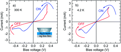
We studied resistive switching in voltage biased nanojunctions created between inert metallic tips and 10–100 nm thick Ag2S surface layers deposited on Ag thin film samples by using an STM setup as illustrated schematically in the inset of Fig. 1(a). While longer sulfur deposition times resulted in semiconducting Ag2S layers in agreement with previous reports,18–20 below an approximate thickness of 20 nm, metallic conductance with technologically optimal device resistances was found over the wide temperature range of 4.2–300 K (ref. 30) both in the ON and OFF states. These characteristics enabled fast operation by nanosecond voltage pulses. Here we focus on switching phenomena observed in all-metallic junctions. We used a superconducting Nb tip to study the nonlinear differential conductance on the voltage scale of the superconducting gap, eV ≤ Δ = 1.4 meV ≪ Vth. By utilizing the theory of charge conversion at the interface of a normal metal and a superconductor31–34 we quantitatively evaluate the reconfiguration of the conducting channels in the nanojunction and thus demonstrate that resistive switching takes place in highly transparent devices with an effective junction area of 2–5 nm in diameter.
Numerous nanoscale contacts with reproducible I–V characteristics were created by gently touching the sample surface with a mechanically sharpened PtIr or Nb tip. The ON and OFF state resistances RON and ROFF were probed in a narrow voltage window of ±50 mV ≪ Vth. For more experimental details see the ESI† and ref. 30 and 35.
A typical room temperature I–V trace is shown in Fig. 1(a) for a PtIr tip. A linear current–voltage dependence was observed when an increasing positive voltage on the Ag electrode in the high resistance (ROFF ≈ 0.5 kΩ) state was applied. At Vth ≈ 300 mV the junction switches to its low resistance ON state (RON ≈ 0.1 kΩ). At a subsequent decrease of the bias a linear dependence is observed until the negative threshold voltage is reached where the OFF state is restored. The slight reverse of the onset of OFF to ON switching arises due to the compensation for the finite 50–200 Ω serial resistance of the voltage biasing circuit. By limiting the current in the ON state, this serial resistance also plays a role in maintaining the stability of the junctions. The observed switching scheme is ideal for memory applications, as the device can be switched between the two states at a reasonably high bias while RON and ROFF are optimal for fast readout at low bias.
A similar I–V trace is obtained at 4.2 K as shown in Fig. 1(b) testifying to the metallic nature of the system. The linear ON and OFF traces and the wide range of operation temperatures contradict the thermally activated ionic migration in bulk Ag2S.29 The observed metallic behavior is consistent with first-principles calculations applicable to a thin surface layer of Ag2S deposited on bulk Ag which is expected to undergo a structural phase transition called spontaneous metallization.23 Next, we investigated this metallized state experimentally by replacing the PtIr tip by superconducting Nb and utilizing point contact Andreev reflection (PCAR) spectroscopy.31–34
This method is inspired by the fact that linear conductance measurements alone cannot distinguish between fundamentally different types of junctions exhibiting the same conductance. The conductance of a nanoscale device is given as G = 2e2/hMT, where T is the average electron transmission probability across the device and M is the number of open conductance channels.36,37 The latter is approximated as M ≈ (πd/2λF)2, where d is the device diameter and λF is the Fermi wavelength which is ≈0.4 nm in bulk Ag. This simplified picture shows that a kΩ device resistance may as well correspond to a large area tunnel junction (d ≫ λF) with very small transmission probability (T ≪ 1) or, alternatively, to a truly nanometer-scale junction with only a few well transmitting (T ≈ 1) conductance channels. PCAR measurements performed on the voltage scale of Δ can distinguish between these extremities via the nonlinear transport properties of a point contact connecting a normal metal (N) and a superconductor (S).31 The transmission can be evaluated by fitting the voltage dependence of differential conductance with the model of Blonder, Tinkham and Klapwijk (BTK).32,33
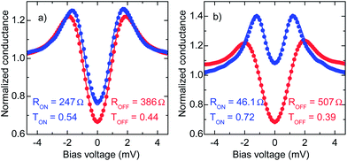
Fig. 2 shows the finite bias differential conductance of the ON and OFF states in two representative junctions exhibiting a minor change [Fig. 2(a)] and an order of magnitude larger change [Fig. 2(b)] in the normal state differential conductance (GN) upon switching. The typical switching threshold voltages of Vth ≈ 300–800 mV are well separated from the N–S features taking place at the voltage scale of Δ. The effective transmissions were determined by fitting the differential conductance curves against the modified version of the BTK theory, incorporating a Γ broadening parameter, as defined in ref. 38, which is also necessary to account for contact diameters comparable to the electronic mean free path.39 With this extension the spin degenerate model contains five parameters: the temperature, Δ, GN, Γ and T. A numerically reliable and physically meaningful fitting procedure, however, requires the reduction of an extended parameter space to a minimum set of key parameters. After taking extra care of the proper thermal anchoring of the device leads in our 4He cryostat we fixed the temperature value to 4.2 K. Finite bias tunneling measurements (Rcontact > 100 kΩ) carried out on Ag–Ag2S–Nb samples and on clean Au foils revealed that the bulk value of Δ = 1.4 meV was also a good approximation in our point contact arrangement. In these data, Γ stayed below 5% of Δ quantifying the voltage noise of our setup. After evaluating GN from the high bias linear slopes of the raw I–V traces, the BTK fittings were run with two free parameters T and Γ.
In device 1 [Fig. 2(a)] RON = 247 Ω and ROFF = 386 Ω. The corresponding transmission probabilities are 0.54 and 0.44, whereas the effective numbers of open conductance channels, estimated as M = GN/G0T, are 118 and 62, respectively. This shows that both the ON and OFF states are characterized by rather large transmission values and the 56% change of the conductance between the two states is equally attributed to the variations in M and T. In device 2 [Fig. 2(b)] the order of magnitude change in GN (GON/GOFF = 11) is accompanied by a large change in M (MON/MOFF = 6.2) and a minor change in T (TON/TOFF = 1.8). The ON and OFF state effective contact diameters were estimated to be dON = 2.7 nm and dOFF = 2 nm in device 1 and dON = 5 nm and dOFF = 2.1 nm in device 2, demonstrating that resistive switching takes place in truly nanometer-scale junctions.
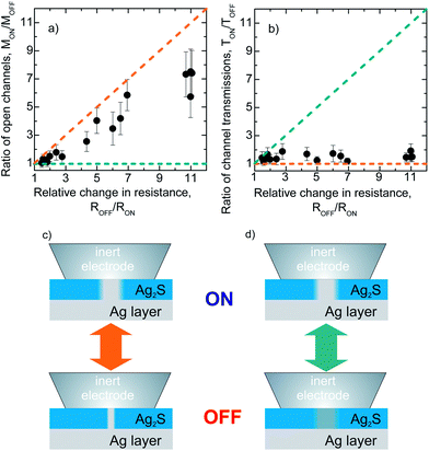
In order to verify the statistical relevance of these findings, T and d were evaluated for various junctions yielding to TON = 0.62 ± 0.1 and TOFF = 0.42 ± 0.07 at effective junction diameters of d = 2–5 nm. Fig. 3 shows the relative changes in T and M upon switching as a function of the resistance ratio of the corresponding ON and OFF states. The two limiting cases of the unchanged transmissions and unchanged channel numbers are indicated in Fig. 3(a) and (b) by the orange and green dashed lines and are also schematically illustrated in Fig. 3(c) and (d), respectively. The numerical accuracy of T is 20% in the OFF states and better than 5% in the ON states as explained in the ESI† and is indicated by the error bars in Fig. 3(a) and (b). In the studied junctions with ON and OFF state resistances of 50–1000 Ω, Γ is 50–15% of Δ, respectively. These values are significantly higher than those obtained in the tunneling regime, which agree with previous studies carried out on various diffusive systems.39 This indicates that in spite of the small junction diameters, electron transport is not entirely ballistic due to the rather short mean free path of 1.8 nm in Ag2S.40
Our analysis shows that (i) regardless of the relative change in their resistances, all devices exhibit high transmission probabilities in both states corresponding to metallic conductances and (ii) their conductance changes can be attributed to a variation in M while T is less significantly changed during the switching. These results give clear evidence that the metallic channels are not completely destructed when the device is switched off, only their effective cross section is reduced while the highly transmitting nature is preserved. This is in good agreement with the presence of spontaneously metallized Ag2S channels23 and is in contrast with the simplified picture of the formation and complete destruction of pure Ag nanofilaments. While the amplitude of the voltage bias signal influences the actual ON and OFF state resistances [see Fig. 4(a) in ref. 21] our experience shows that the metallic nature of the OFF state is preserved throughout a broad range of biasing conditions. The above characteristics make Ag2S based devices particularly suitable to build resistive memory elements with technologically ideal resistances of ≤1 kΩ and diameters well below the resolution of current lithographic techniques. Note that tunnel junctions of similar sizes would yield resistances with a larger order of magnitude, challenging their fast electronic applications.
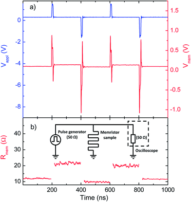
Finally we demonstrated that the resistive switching of the investigated nanometer-scale metallic channels is a fast process taking place on a nanosecond time scale. Real-time pulsed measurements were performed in vacuum conditions at room temperature by connecting the Ag–Ag2S–PtIr junction to an arbitrary waveform generator and a digital oscilloscope of 2 ns time resolution via a transmission line in a circuit schematically illustrated in the inset of Fig. 4(b). Subsequent switching between the ON and OFF states was achieved by voltage pulses of 10 ns duration, 1.5 V amplitude and alternating sign. Between the pulses the device resistance was monitored by applying a 350 mV dc bias. The blue line in Fig. 4(a) shows the applied pulse train in an open circuit configuration when the sample is not connected and the transmission line is terminated by an open end resulting in the total reflection of the pulses. In comparison, the red line corresponds to the situation when the transmitted signal from the pulse generator to the scope is superimposed on a partially reflected signal emerging due to the finite resistance of the memristor device. Fig. 4(b) shows the calculated resistances of ROFF = 20 Ω and RON = 12 Ω. The subsequent, reproducible resistance plateaus are well separated both from each other and from the noise floor of the measurement, satisfying the two most profound requirements of memory applications. While fast pulsing measurements favor contact impedances close to 50 Ω, fast switching at higher contact resistances were also observed, though with lower resolution.
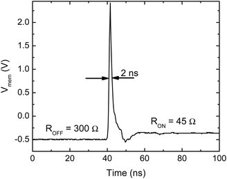
While the ≥1.5 ns rise/fall times of our arbitrary waveform generator limit the investigation of shorter time domains by voltage pulses of alternating sign, the single shot experiment shown in Fig. 5 demonstrates that resistive switching in Ag2S can also be induced by voltage pulses as short as 500 ps. Such measurements were carried out by using a custom built rise time avalanche pulse generator specified to provide unipolar voltage pulses of 500 ps width and ≤10 V amplitude.41 The low bias readout between the short pulses and the subsequent reinitialization of the OFF state was performed by a variable dc offset added to the biasing circuit as explained in the ESI.† Whereas the real-time response of the device is not fully resolved in the experiment due to instrumental and circuit limitations, it is evident that a sub-nanosecond pulse can initiate resistive switching.
In conclusion, we studied the resistive switching of Ag–Ag2S–Me memristive nanojunction devices. We showed that by suitable sample preparation reproducible resistive switching and readout can be performed where both the ON and OFF states are metallic, characterized by technologically optimal ≤1 kΩ resistances and similar device functionalities down to cryogenic temperatures. We introduced PCAR spectroscopy to determine the size and transmission probabilities of the active volume of the devices which revealed a small number of highly transmitting nanoscale conducting channels with reduced but not completely dissolved junction area in the OFF state. The relatively low resistance ON and OFF states enable fast operation: our devices can be switched by nanosecond voltage pulses at room temperature. The achieved ROFF/RON ratios as high as 10 satisfy the basic requirement of reliable read-out.14 These results suggest that Ag2S represents a promising material basis for a future generation of high speed resistive switching memory devices overriding the downscaling limitations of current CMOS technology.
Acknowledgements
Enlightening discussions with Ádám Szüllő and his circuit designing contribution to the fast pulsing experiments are acknowledged. This work has been supported by the Hungarian research funds OTKA CNK80991, K105735, TÁMOP 4.2.1.B-09/1-2010-0002. M.C. is a grantee of the Bolyai János Research Scholarship of the HAS and acknowledges financial support of the European Union 7th Framework Programme (Grant no. 293797).References
- International Technology Roadmap for Semiconductors, 2012.
- R. Chau, B. Doyle, S. Datta, J. Kavalieros and K. Zhang, Nat. Mater., 2007, 6, 810–812 CrossRef CAS PubMed.
- K. Kuhn, IEEE Trans. Electron Devices, 2012, 59, 1813–1828 CrossRef CAS.
- J. R. Heath and M. A. Ratner, Phys. Today, 2003, 56, 43 CrossRef CAS PubMed.
- C. Schirm, M. Matt, F. Pauly, J. C. Cuevas, P. Nielaba and E. Scheer, Nat. Nanotechnol., 2013, 8, 645 CrossRef CAS PubMed.
- J. J. Yang, D. B. Strukov and D. R. Stewart, Nat. Nanotechnol., 2013, 8, 13–24 CrossRef CAS PubMed.
- K. Terabe, T. Hasegawa, T. Nakayama and M. Aono, Nature, 2005, 433, 47–50 CrossRef CAS PubMed.
- D. B. Strukov, G. S. Snider, D. R. Stewart and R. S. Williams, Nature, 2008, 453, 80–83 CrossRef CAS PubMed.
- R. Waser and M. Aono, Nat. Mater., 2007, 6, 833–840 CrossRef CAS PubMed.
- K. Terabe, T. Hasegawa, C. Liang and M. Aono, Adv. Mater., 2007, 8, 536–542 CAS.
- M. Aono and T. Hasegawa, IEEE Proc., 2010, 98, 2228–2236 CrossRef CAS.
- E. Linn, R. Rosezin, C. Kugeler and R. Waser, Nat. Mater., 2010, 9, 403–406 CrossRef CAS PubMed.
- A. C. Torrezan, J. P. Strachan, G. Medeiros-Ribeiro and R. S. Williams, Nanotechnology, 2011, 22, 485203 CrossRef PubMed.
- R. Waser, R. Dittmann, G. Staikov and K. Szot, Adv. Mater., 2009, 21, 2632–2663 CrossRef CAS.
- L. Chua, IEEE Trans. Circuit Theory, 1971, 18, 507–519 CrossRef.
- Y. V. Pershin and M. Di Ventra, Adv. Phys., 2011, 60, 145–227 CrossRef.
- K. Terabe, T. Nakayama, T. Hasegawa and M. Aono, J. Appl. Phys., 2002, 91, 10110–10114 CrossRef CAS PubMed.
- M. Morales-Masis, S. J. van der Molen, W. T. Fu, M. B. Hesselberth and J. M. van Ruitenbeek, Nanotechnology, 2009, 20, 095710 CrossRef CAS PubMed.
- M. Morales-Masis, H.-D. Wiemhöfer and J. M. van Ruitenbeek, Nanoscale, 2010, 2, 2275–2280 RSC.
- M. Morales-Masis, S. J. van der Molen, T. Hasegawa and J. M. van Ruitenbeek, Phys. Rev. B: Condens. Matter Mater. Phys., 2011, 84, 115310 CrossRef.
- A. Geresdi, A. Halbritter, A. Gyenis, P. Makk and G. Mihály, Nanoscale, 2011, 3, 1504–1507 RSC.
- Z. Xu, Y. Bando, W. Wang, X. Bai and D. Golberg, ACS Nano, 2010, 4, 2515–2522 CrossRef CAS PubMed.
- Z. Wang, T. Kadohira, T. Tada and S. Watanabe, Nano Lett., 2007, 7, 2688–2692 CrossRef CAS PubMed.
- Z. Wang, T. Gu, T. Tada and S. Watanabe, Appl. Phys. Lett., 2008, 93, 152106 CrossRef PubMed.
- J. J. T. Wagenaar, M. Morales-Masis and J. M. van Ruitenbeek, J. Appl. Phys., 2012, 111, 014302 CrossRef PubMed.
- T. Hasegawa, T. Ohno, K. Terabe, T. Tsuruoka, T. Nakayama, J. K. Gimzewski and M. Aono, Adv. Mater., 2010, 22, 1831–1834 CrossRef CAS PubMed.
- T. Ohno, T. Hasegawa, T. Tsuruoka, K. Terabe, J. K. Gimzewski and M. Aono, Nat. Mater., 2011, 10, 591–595 CrossRef CAS PubMed.
- M. D. Pickett, G. Medeiros-Ribeiro and R. S. Williams, Nat. Mater., 2013, 12, 114–117 CrossRef CAS PubMed.
- A. Nayak, T. Tamura, T. Tsuruoka, K. Terabe, S. Hosaka, T. Hasegawa and M. Aono, J. Phys. Chem. Lett., 2010, 1, 604–608 CrossRef CAS.
- A. Geresdi, A. Halbritter, E. Szilágyi and G. Mihály, MRS Proceedings, 2011, 1331 Search PubMed.
- A. F. Andreev, Soviet Physics - JETP, 1964, 19, 1228 Search PubMed.
- G. E. Blonder, M. Tinkham and T. M. Klapwijk, Phys. Rev. B: Condens. Matter Mater. Phys., 1982, 25, 4515–4532 CrossRef CAS.
- J. C. Cuevas, A. Martín-Rodero and A. Levy Yeyati, Phys. Rev. B: Condens. Matter, 1996, 54, 7366–7379 CrossRef CAS.
- R. J. Soulen, J. M. Biers, M. S. Ofosky, B. Nadgorny, T. Ambrose, S. F. Cheng, P. R. Broussard, C. T. Tanaka, J. Nowak, J. S. Moodera, A. Barry and J. M. D. Coey, Science, 1998, 282, 85–88 CrossRef CAS.
- E. Kótai, Nucl. Instrum. Methods Phys. Res., Sect. B, 1994, 85, 588–596 CrossRef.
- R. Landauer, Philos. Mag., 1970, 21, 863–867 CrossRef CAS.
- Y. V. Nazarov and Y. M. Blanter, Quantum Transport: Introduction to Nanoscience, Cambridge University Press, 2009 Search PubMed.
- A. Pleceník, M. Grajcar, Š. Beňačka, P. Seidel and A. Pfuch, Phys. Rev. B: Condens. Matter, 1994, 49, 10016–10019 CrossRef.
- A. Geresdi, A. Halbritter, M. Csontos, S. Csonka, G. Mihály, T. Wojtowicz, X. Liu, B. Jankó and J. K. Furdyna, Phys. Rev. B: Condens. Matter Mater. Phys., 2008, 77, 233304 CrossRef.
- J. Zemek, P. Jiricek, S. Hucek, A. Jablonski and B. Lesiak, Surf. Sci., 2001, 473, 8–16 CrossRef CAS.
- J. Williams, Linear Technology Application Note, 1991, vol. 47 Search PubMed.
Footnote |
| † Electronic supplementary information (ESI) available: Sample preparation and structural characterization as well as involved experimental and analysis details. See DOI: 10.1039/c3nr05682a |
| This journal is © The Royal Society of Chemistry 2014 |

