 Open Access Article
 This Open Access Article is licensed under a
 Creative Commons Attribution 3.0 Unported Licence
The renaissance of hybrid solar cells: progresses, challenges, and perspectives
Feng
Gao
*a,
Shenqiang
Ren
*b and
Jianpu
Wang
*c
aDepartment of Physics, Chemistry and Biology (IFM), Linköping University, Linköping 58183, Sweden. E-mail: fenga@ifm.liu.se
bDepartment of Chemistry, University of Kansas, Lawrence, KS 66045, USA. E-mail: shenqiang@ku.edu
cCavendish Laboratory, J J Thomson Avenue, Cambridge CB3 0HE, UK. E-mail: jw479@cam.ac.uk
First published on 12th June 2013
Abstract
Solution-processed hybrid solar cells, a blend of conjugated polymers and semiconducting nanocrystals, are a promising candidate for next-generation energy-conversion devices. The renaissance of this field in recent years has yielded a much deeper understanding of optoelectronic interactions in organic–inorganic hybrid systems. In this article, we review the state-of-the-art progress in hybrid bulk heterojunction solar cells, covering new materials design, interfacial interaction, and processing control. Furthermore, critical challenges that determine photovoltaic performance and prospects for future directions are discussed.
 Feng Gao | Feng Gao is a Marie Curie research fellow at the Department of Physics, Chemistry and Biology (IFM) at Linköping University (Sweden), working on organic electronics and bioelectronics. In his PhD work at the Cavendish Laboratory of the University of Cambridge (UK), he studied device physics of polymer-based solar cells. Before that, he obtained his BS and MS degrees in physics from Nanjing University (China). |
 Shenqiang Ren | Shenqiang Ren is an assistant professor of chemistry at the University of Kansas (USA) leading the renewable and emerging nanomaterials (REN) group, working in the renewable energy area. He obtained his PhD in Materials Science at the University of Maryland, College Park (USA), and worked as a postdoc fellow on hybrid photovoltaic solar cells at MIT (USA) before his current position. |
 Jianpu Wang | Jianpu Wang has been a postdoctoral research associate in Cavendish Laboratory, University of Cambridge since 2009. His research interests are organic/solution processable semiconductor devices and device physics. He did his PhD study in the same laboratory from 2006 to 2009, when he investigated organic semiconductor/inorganic nanocrystal devices. Prior to his PhD, he worked as a research engineer in Samsung Electronics in South Korea in 2003–2006, for developing ink-jet printing technology. |
Broader contextGlobal warming and fossil fuel depletion are driving humans to explore green and renewable energy sources. Solution-processed hybrid photovoltaics, a blend of conjugated polymers and semiconducting nanocrystals, are a promising candidate to convert sunlight into electricity. Hybrid photovoltaics combine the unique advantages of organic and inorganic semiconductors, i.e., cost-effective manufacturing processes, tunable absorption regimes, high charge carrier mobility, and high dielectric constant. The study of hybrid photovoltaics is multidisciplinary, covering organic and inorganic semiconducting materials, surface ligand design, device structure design, and efficiency optimization. This review article gives an in-depth understanding of photovoltaic processes in the operation of hybrid photovoltaics, and relates primary studies with these processes. Current challenges of hybrid photovoltaics are also discussed, and directions for further research are proposed. |
1 Introduction
Global warming and fossil fuel depletion are driving humans to explore green and renewable energy sources. Among others, solar energy is recognized as a secure and sustainable energy that can reduce carbon emissions. Although the current solar cell market is dominated by inorganic photovoltaic (PV) cells, emerging technologies, such as dye-sensitized solar cells1 and organic solar cells,2–4 have also attracted increasing attention.Compared with their inorganic counterparts, organic PVs (OPVs) have some unique advantages. For example, organic materials are usually solution-processable. Therefore, low-cost manufacturing methods, e.g. inkjet printing and roll-to-roll deposition, can be employed. In addition, organic materials have high absorption coefficients so that a layer of a few hundred nanometers can absorb all the light at their peak absorption wavelengths. As a result, OPVs could potentially provide electricity at a lower cost than inorganic PVs.
Photon absorption in organic materials produces strongly bound excitons, rather than free charges in inorganic materials. Therefore, a driving force is needed in OPV devices to split excitons into free charge carriers. This driving force is provided by the energetic offset between two materials in the bulk heterojunction (BHJ) structure, where the donor and acceptor materials are intimately mixed together.3,4
Currently, there are three types of polymer-based BHJ OPVs intensively investigated in the research community, including polymer:fullerene blends, polymer:polymer blends, and polymer:nanocrystal blends. Since the first demonstration of a successful polymer:fullerene device in 1995,4 such devices have consistently shown the highest efficiency among all BHJ OPVs, with the recently reported PCE approaching 10%.5 The commonly used fullerenes are soluble [6,6]-phenyl-C61-butyric acid methyl ester (PCBM) and [6,6]-phenyl-C71-butyric acid methyl ester (PC70BM). The disadvantage of polymer:fullerene devices is that the fullerene absorption is poor in the solar spectrum range.6 In this regard, the polymer:polymer combination offers potential advantages over the polymer:fullerene blends in that the bandgap of the polymer is easily tuned, and hence it is possible to design a device covering a wider solar spectrum. However, limited by geminate pair separation,7,8 the efficiency of the polymer:polymer device is relatively low, with the highest reported PCE of around 2%.9
In addition to the tunable bandgap, solution-processable nanocrystals (NCs) have further advantages like large dielectric constants and tunability of the NC shape. As we will discuss in detail later, the higher dielectric constant of inorganic NCs (e.g. ∼10.4 for CdSe compared with ∼3.9 for PCBM)10 decreases the coulombic attraction between electrons and holes, facilitating charge separation. The tunability of the NC shape could further promote charge transport. As a result, NCs are supposed to be an ideal component for BHJ OPVs. The first polymer:NC hybrid solar cell was demonstrated in 1996 by Greenham et al., who used CdSe nanodots as the acceptor and MEH-PPV as the donor (see Fig. 1 for chemical structures of the polymers mentioned in this article).11 The power conversion efficiency (PCE) of their device was low, which was attributed to poor charge transport through CdSe nanodots. Afterwards, much effort has been devoted to improving the charge transport by tuning the NC shape as well as controlling the nanomorphology.12–16 This engineering work resulted in steady improvement in the device efficiency, with PCE reaching 2.6% in 2006.17 In 2010 Dayal et al. used a low bandgap polymer (PCPDTBT) as the donor, and achieved an efficiency over 3%.18 See Table 1 for a selection of hybrid PV performance based on CdSe NCs.
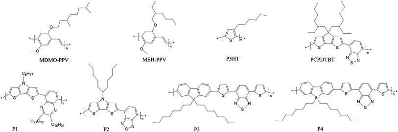 | ||
| Fig. 1 Chemical structures of the polymers discussed in this article. | ||
| Shape | Ligand | Polymer | NCs (wt%) | Light intensityb (mW cm−2) | J SC (mA/cm2) | V OC (V) | FF | PCE (%) | Ref. | Year |
|---|---|---|---|---|---|---|---|---|---|---|
| a Abbreviations: JSC = short-circuit current; VOC = open-circuit voltage; FF = fill factor; ND = nanodot; NR = nanorod; TP = tetrapod; BA = butylamine; HA = hexanoic acid; tBT = tert-butylthiol; dithiol = benzene-1,3-dithiol. b AM 1.5 conditions unless otherwise stated. c Monochromatic illumination at 514 nm. d Calculated based on the information provided in the original paper. e Large size: 7.1 nm. f A ZnO layer between the active layer and the cathode was used as the optical spacer and hole-blocking layer. The efficiency was 2.7% without the ZnO layer. g Relatively small size: 8 × 13 nm. h In the form of fibrils. i Careful NC washing before pyridine treatment. j NDs:NRs = 27:63 by weight. | ||||||||||
| NDs | Pyridine | MEH-PPV | 90 | 0.5c | 0.01c,d | 0.50c | 0.26 | 0.26c,d | 11 | 1996 |
| NDs | Pyridine | MEH-PPV | 86 | 100 | 2.0 | 0.90 | 0.47 | 0.85 | 137 | 2006 |
| NDs | Amine (BA) | P3HT | 89 | 100 | 6.9 | 0.55 | 0.47 | 1.8 | 108 | 2009 |
| NDs | Acid (HA) | P3HT | 87 | 100 | 5.8 | 0.62 | 0.56 | 2.0 | 15 | 2010 |
| NDs | Thiol (tBT) | P3HT | 89 | 100 | 5.6 | 0.80 | 0.43 | 1.9 | 113 | 2012 |
| NDse | Acid (HA) | PCPDTBT | 90 | 100 | 8.7 | 0.63 | 0.56 | 3.1 | 140 | 2011 |
| NDs | Pyridine | PCPDTBT | 90 | 100 | 9.2f | 0.78f | 0.49 | 3.5f | 91 | 2012 |
| NRsg | Pyridine | P3HT | 80 | 0.48c | 0.03c | 0.57c | 0.49 | 1.8c,d | 86 | 1999 |
| NRs | Pyridine | P3HT | 90 | 96.4 | 5.7 | 0.70 | 0.40 | 1.7 | 12 | 2002 |
| NRs | Pyridine | P3HTh | 90 | 92 | 8.8 | 0.62 | 0.50 | 2.6 | 17 | 2006 |
| NRs | Pyridine and dithiol | P3HT | 100 | 9.7 | 0.55 | 0.49 | 2.6 | 112 | 2010 | |
| NRs | Pyridinei | PCPDTBT | 87 | 100 | 12.1 | 0.63 | 0.45 | 3.4 | 90 | 2012 |
| NRs and NDsj | Pyridine | PCPDTBT | 90 | 100 | 13.9 | 0.48 | 0.51 | 3.5 | 141 | 2012 |
| TPs | Pyridine | MDMO-PPV | 86 | 93 | 7.3 | 0.65 | 0.35 | 1.8 | 13 | 2003 |
| TPs | Pyridine | P3 | 86 | 100 | 7.2 | 0.95 | 0.38 | 2.4 | 87 | 2006 |
| TPs | Pyridine | PCPDTBT | 90 | 100 | 9.0 | 0.67 | 0.51 | 3.1 | 18 | 2010 |
| Hyper-branched | Pyridine | P3HT | 100 | 7.1 | 0.60 | 0.51 | 2.2 | 14 | 2007 | |
Before 2009, few hybrid solar cells based on NCs other than CdSe could show efficiencies over 2%. It seemed that CdSe was the only option for efficient hybrid PVs. However, there has been a ‘quantum leap’ in recent years for these NCs, with several of them demonstrating efficiencies around 3% (see Table 2 for a selection of hybrid PV performance based on NCs other than CdSe).19–21 In 2011, using P3HT and CdS NCs, Ren et al. reported a high efficiency of 4.1%, which is currently the record efficiency for hybrid PVs.16 Motivated by these recent developments, we believe that it is helpful to reconsider the strengths and limitations of hybrid PVs, aiming for further improvement of the device performance.
| NCs | Ligand | Polymer | NCs (wt%) | Light intensityb (mW cm−2) | J SC (mA cm−2) | V OC (V) | FF | PCE (%) | Ref. | Year |
|---|---|---|---|---|---|---|---|---|---|---|
| a Abbreviations: JSC = short-circuit current; VOC = open-circuit voltage; FF = fill factor; ND = nanodot; NR = nanorod; TP = tetrapod; NW = nanowire; BA = butylamine; dithiol = benzene-1,3-dithiol; EDT = 1,2-ethanedithiol; OA = oleic acid. b AM 1.5 conditions unless otherwise stated. c In situ growth of NCs in the polymer matrix. d An average value calculated based on the information provided in the original paper. e Illuminated using a white LED. f AM 1 conditions. | ||||||||||
| CdTe NRs | Pyridine | MEH-PPV | 90 | 100 | 0.49 | 0.37 | 0.27 | 0.05 | 26 | 2004 |
| CdTe TPs | Pyridine and dithiol | P7 | 80 | 100 | 7.23 | 0.79 | 0.56 | 3.2 | 19 | 2011 |
| PbS NDs | N/Ac | MEH-PPV | 50–60 | 5 | 0.13 | 1.0 | 0.28 | 0.7 | 40 | 2005 |
| PbS NDs | Amine (BA) | P1 | 90 | 100 | 4.2 | 0.38 | 0.34 | 0.55 | 41 | 2010 |
| PbS NDs | Thiol (EDT) | PDTPBT | 90 | 100 | 13.1 | 0.57 | 0.51 | 3.8 | 20 | 2011 |
| PbSe NDs | Acid (OA) | P3HT | 80 | 100 | 1.1 | 0.35 | 0.37 | 0.14 | 28 | 2006 |
| Si NDs | P3HT | 50 | 100 | 3.8 | 0.8 | 0.47 | 1.47 | 64 | 2010 | |
| CuInS2 NDs | N/Ac | P4 | 90d | 100 | 10.3 | 0.54 | 0.5 | 2.8 | 21 | 2011 |
| GaAs NWs | P3HT | 50 | 70e | 5.8 | 0.59 | 0.4 | 1.95 | 68 | 2011 | |
| CdS TPs | Pyridine | MEH-PPV | 86 | 100 | 2.96 | 0.85 | 0.47 | 1.17 | 69 | 2007 |
| CdS NRs | N/Ac | P3HT | 100 | 9 | 0.65 | 0.48 | 2.9 | 70 | 2009 | |
| CdS NDs | Amine (BA) and thiol (EDT) | P3HT | 80 | 100 | 10.9 | 1.1 | 0.35 | 4.1 | 16 | 2011 |
| ZnO NDs | MDMO-PPV | 67 | 71 | 2.4 | 0.81 | 0.59 | 1.6 | 71 | 2004 | |
| ZnO NDs | N/Ac | P3HT | 50 | 100 | 5.2 | 0.75 | 0.52 | 2.0 | 76 | 2009 |
| TiO2 NDs | P3HT | 60 | 100f | 2.76 | 0.44 | 0.36 | 0.42 | 77 | 2004 | |
| TiO2 NRs | N3-dye | P3HT | 50 | 100 | 4.33 | 0.78 | 0.65 | 2.2 | 82 | 2009 |
This article starts with a brief introduction of NCs and fundamental processes involved in the operation of a BHJ device. This is followed by the efforts that the hybrid PV research community has made to improve the device performance. We highlight the factors that limit the device efficiency as well as the strategies to overcome these limiting factors. We focus on the hybrid PVs where colloidal NCs are blended with conjugated polymers. The other types of hybrid PVs where rigid nanoporous or nanorod structures are filled with a polymer have been recently reviewed elsewhere.22,23
2 Hybrid PVs
2.1 Nanocrystals
NCs have properties that are different from the bulk material, mainly due to quantum confinement. The electron–hole pair (exciton) in a semiconductor is bound within a characteristic length, known as the Bohr radius, which is a material-dependent property. For example, the Bohr diameters are 10.6 nm for CdSe, 15.0 nm for CdTe, and 40 nm for PbS.24 When the size of a semiconductor NC is smaller than the Bohr diameter, the charge carriers in NCs are spatially confined. In this case, the energy of the charge carriers will be raised, and the properties change from the bulk regime to the quantum confinement regime. In the quantum confinement regime, the optical and electrical properties will be dependent on the NC size. These tunable properties of semiconductor NCs make them very interesting for optoelectronic applications.NCs with different sizes and shapes can be synthesized in solution. The surfaces of the NCs are usually covered with organic ligands, which make the NCs solution-processable. With decreasing size, the number of surface atoms increases, which also affects the optical and electrical properties of NCs. The atoms on the NC surface are incompletely bonded with the crystal lattice, which disrupts the crystalline periodicity and leaves ‘dangling orbitals’ on the surface atoms. If the energy states of these unpassivated orbitals (the atomic orbitals formed by the incomplete bonding structure at the surface)25 are within the NC bandgap, they can serve as charge traps, which increase the possibility of non-radiative decay. When the NCs are covered with organic ligands, these surface dangling bonds are passivated by bonding with ligands, hence minimizing the intra-bandgap defect states.
2.2 Photovoltaic processes in BHJ OPVs
A summary of the processes involved in the photovoltaic effect is shown in Fig. 2 from a kinetic perspective, where photon absorption by the NC phase is neglected for clarity. (i) The absorption of the light generates excitons, which can (ii) thermally diffuse into the donor–acceptor interface. If the excitons fail to find an interface within their lifetime, they will decay to the ground state. At the interface, (iii) fast exciton dissociation takes place by transferring the electron to the acceptor phase. Subsequently, with the help of the internal field, (iv) the separated carriers are transported towards the electrodes, producing photocurrent. During their transport to the electrodes, the carriers might decay via non-geminate recombination, e.g. bimolecular recombination or trap-assisted recombination.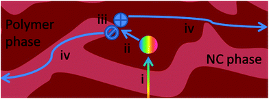 | ||
| Fig. 2 Schematic illustration of the processes involved in the photovoltaic effect from a kinetic point of view. (i) Light absorption leads to exciton generation; (ii) exciton diffusion into the polymer:NC interface; (iii) charge transfer from the polymer phase to the NC phase; and (iv) charge transport to electrodes. | ||
2.3 Exciton generation in hybrid PVs
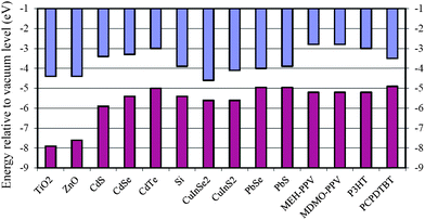 | ||
| Scheme 1 Energy levels of the selected semiconducting NCs and polymers considered in this article. The energy levels are taken from ref. 29–36. Note that the NC energy levels depend on the NC size as well as measurement techniques. | ||
CdTe NCs have an absorption spectrum extending into the near infrared (NIR) range, making them more suitable for hybrid PVs in terms of exciton generation. However, the first hybrid solar cell based on CdTe NCs showed a very low efficiency of 0.05%.26 Subsequently, a series of hybrid PVs based on MEH-PPV and CdSexTe1−x tetrapod NCs were investigated in detail, and it was found that the device performance decreased with increasing Te content.37 Based on cyclic voltammetry measurements, the highest occupied molecular orbital (HOMO) level of CdTe NCs was determined to be −5.0 eV, which is higher than (or close to) that of the donor polymer, e.g. MEH-PPV or P3HT. Therefore, it was proposed that the poor efficiency was due to energy transfer between the polymer and CdTe NCs. However, there are other publications reporting low HOMO levels of −5.5 eV or even −5.8 eV for CdTe NCs.19,38 The discrepancy might be caused by different sizes and/or shapes of the samples in different measurements, as well as the fact that cyclic voltammetry is not an accurate method to determine the band position. If the CdTe HOMO level is as low as −5.5 eV, CdTe NCs might still be a good candidate as an acceptor material in hybrid PVs. Recently, Chou and co-workers reported a significantly improved efficiency of 3.2% for CdTe-based hybrid solar cells, using a monoaniline-capped polymer as the donor.19 This might indicate that energy transfer is not the main problem for the poor efficiency in previous studies.
Further extension of the absorption spectrum into the infrared regime could be achieved using PbSe or PbS NCs. Sargent and co-workers demonstrated hybrid PVs based on PbS and MEH-PPV.27,39 Unfortunately, the device efficiency was very low, showing no benefit from the infrared absorption. Watt et al. employed a surfactant-free NC synthesis approach, where they synthesized PbS NCs directly in the MEH-PPV matrix, and obtained improved efficiency (0.7% under AM 1.5, 5 mW cm−2 illumination).40 Ginger and co-workers used a new donor–acceptor conjugated polymer (P1 in Fig. 1) as the donor in the PbS-based hybrid PVs, and obtained an efficiency of 0.5% under normal illumination conditions (AM 1.5, 100 mW cm−2).41 More recently, by blending PbS NCs with a low bandgap polymer (P2 in Fig. 1), Prasad and co-workers significantly improved the device efficiency to a high value of 3.78%.20
In spite of the improvement in PbS-based hybrid solar cells, the device engineering on PbSe-based hybrid PVs has been difficult, with a low power conversion efficiency of ∼0.1% to date.28,42–44 Ginger and co-workers used photoinduced absorption (PIA) spectroscopy to uncover the reason behind this poor efficiency.45 PIA is a quasi-steady-state pump-probe technique, which is useful for detection of long-lived (>10 μs) excited states, such as polarons or triplet excitons. It measures the transmittance difference before and after excitation. If the excitation results in long-lived species, which give rise to new sub-bandgap optical transitions, the absorption of these species will leave non-zero PIA signals in their absorption regime. Fig. 3 shows the PIA signal of P3HT:PbSe blends, together with those of P3HT:CdSe and P3HT:PCBM blends for comparison. The PIA spectra for blends of P3HT with CdSe and with PCBM showed a broad absorption from 1.0 to 2.1 eV, with a maximum at ∼1.25 eV. This agreed well with the polaronic absorption features of P3HT,46 and hence indicated the generation of positive charges in P3HT for these two blends. In contrast, no characteristic P3HT polaronic feature was observed in the P3HT:PbSe case, indicating the absence of charge carrier generation, which explained the poor efficiency of polymer:PbSe blends. However, the absence of long-lived charge transfer in the PIA spectra does not necessarily mean that the device does not work. For example, Ginger and co-workers demonstrated a hybrid solar cell which exhibited photocurrent contribution from the absorption of both the polymer and quantum dot components in the absence of a typical spectral signature of polymer polarons. They proposed that the device worked as a quantum-dot Schottky diode sensitized by energy transfer from the polymer.47 As a side note, although the efficiency of hybrid PVs based on PbSe is low, it has been demonstrated that Pb(Se,S) NC-based quantum dot solar cells show promising efficiency up to 7%.48–53 Interested readers are referred to a commentary by Sargent.54
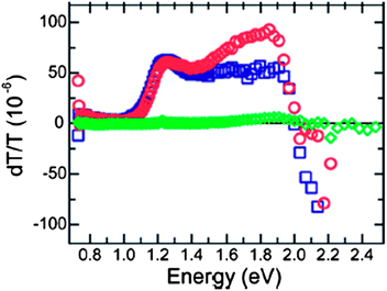 | ||
| Fig. 3 PIA spectra from P3HT blends with PbSe (green diamonds), PCBM (red circles), and CdSe (blue squares). No polaronic features are observed for P3HT:PbSe blends. This indicates little charge carrier generation, explaining the poor device efficiency for polymer:PbSe blends. Reproduced with permission from ref. 45, Copyright 2009, American Chemical Society. | ||
In addition to better absorption, using PbSe and PbS NCs in hybrid OPVs is also motivated by their potential for multiple exciton generation (MEG). MEG is based on utilizing hot carriers to generate one or more additional electron–hole pairs, which can be explained by impact ionization. Nozik proposed that MEG could be greatly enhanced in NCs compared to bulk semiconductors.55 The formation of two or more excitons per absorbed photon for PbSe NCs was demonstrated by different groups using transient absorption measurements.56–58 Recently, Nozik, Beard and co-workers demonstrated the photocurrent enhancement arising from MEG in PbSe quantum dots-based solar cells, as manifested by a peak external quantum efficiency (EQE) exceeding 100%.59 However, the contribution of MEG to the hybrid solar cell efficiency is not confirmed yet, although it was claimed that MEG was observed in MEH-PPV:PbSe devices with an EQE up to 150% at negative biases.42
Another compelling concept for hybrid solar cells with low bandgap NCs is singlet exciton fission.60,61 Singlet exciton fission is a well-established process in organic semiconductors by which a singlet exciton splits to form two triplet excitons on a nearby molecule.62 Singlet exciton fission could potentially overcome the inherently detrimental thermalization losses associated with the high energy exciton of organic semiconductors and the low energy exciton of low bandgap NCs. Pentacene is an attractive material for single exciton fission,63 because its low relaxed triplet exciton energy is less than half of the singlet energy, making the fission process exothermic.60 Greenham and co-workers fabricated hybrid solar cells made of pentacene and PbS NCs, harvesting both triplet excitons created by singlet exciton fission in pentacene and low-energy excitons absorbed by PbS NCs (see Fig. 4 for the device structure and energy diagram).60,61 The application of singlet exciton fission in hybrid solar cells might help to achieve quantum efficiencies over 100%.
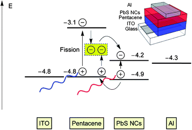 | ||
| Fig. 4 Device structure and energy diagram of hybrid solar cells made of pentacene and PbS NCs. Triplet excitons are created by singlet exciton fission in pentacene and low-energy excitons are absorbed by PbS NCs. Reproduced with permission from ref. 60, Copyright 2012, American Chemical Society. | ||
There are also reports trying to use other low bandgap NCs as the acceptor materials, e.g. Si,29,64 Ge,65 CuInSe2,30,66 CuInS2,21,67 GaAs,68etc. Some of them have demonstrated efficiencies approaching 3%, worthy of further investigation.
In the work by Greenham et al., in addition to CdSe, CdS NCs were also considered as acceptor candidates. However, they found that the polymer photoluminescence (PL) was not completely quenched by CdS NCs, which might be caused by relatively large phase separation. They did not report the device performance using CdS NCs as the acceptor.11 Cao and co-workers were able to overcome this phase separation problem by choosing a suitable solvent, and they observed significant PL quenching of the polymer.69 As a result, a reasonably high efficiency of 1.17% was achieved for the device based on MEH-PPV and CdS tetrapods. Liao et al. made use of the sulfur atoms along the backbone of P3HT as anchorage sites for CdS to nucleate and grow, and they synthesized CdS nanorods using P3HT as a molecular template. Their device showed an improved efficiency of 2.9%.70 More recently, by carefully engineering the NC surface as well as the polymer morphology, Ren et al. reported a promising efficiency of 4.1% for devices based on P3HT and CdS nanodots.16
In spite of their even worse absorption ability than CdS, metal oxides have also attracted intensive interest, due to their low cost and non-toxicity. Janssen and co-workers demonstrated that MDMO-PPV:ZnO blends could give an efficiency of 1.6% under 71 mw cm−2 white light illumination.71 A relatively low NC weight ratio (67%) was used in their experiments, as they noticed that a high concentration of ZnO NCs tended to aggregate in the device. This is because of the poor solubility of ZnO NCs in solvents that dissolve common semiconducting polymers.72 In a subsequent study, they tried to add a surfactant to ZnO, and changed the NC shape and size, aiming at improving the device performance. However, the device efficiency remained at around 1.6%.73 Even if MDMO-PPV was replaced by P3HT, which has higher hole mobility, no improvement in the device performance was obtained.74 Later on, the same group employed a method to in situ generate ZnO NCs inside organic materials,75 and obtained a record efficiency of 2.0% for ZnO-based hybrid PVs.76
In addition to ZnO, TiO2 is also explored as the acceptor material in hybrid PVs, partially because of its success in dye-sensitized solar cells.1 Kwong et al. blended TiO2 NCs with P3HT, where they optimized the solvent and obtained an efficiency of 0.42%.77 In addition to this solvent optimization work, there has been a lot of other device engineering, including in situ generation of TiO2 inside polymers,78,79 and optimization of the NC ligand,80etc. Recently, Chen, Su and co-workers replaced the insulating surfactant on the NC surface with a more conductive ligand, and increased the device efficiency to 1.7%.81 In a subsequent study, they employed a dye to modify the NC surface, which further increased the PCE to 2.2%.82 Although these kinds of devices including dyes could possibly work as solid-state dye-sensitized solar cells, the authors claimed that their devices remained hybrid PVs based on the fact that no contribution from the dye was observed from the EQE spectra. Indeed, there are other TiO2-based solar cells showing obvious evidence to function as solid-state dye-sensitized solar cells.83–85 This is beyond the scope of this article, and interested readers are referred to a recent review for more discussions on this issue.22
Dayal et al. fabricated a device containing PCPDTBT and CdSe tetrapods, which gave a certified efficiency of ∼3.1%, the record efficiency for hybrid solar cells at that time.18 By optimizing the NC surface, Krüger and co-workers pushed this number to 3.4%, where they blended PCPDTBT with CdSe nanorods.90 Xue and co-workers added a thin ZnO nanoparticle layer between the cathode and the active layer, which was a blend of PCPDTBT and CdSe nanodots, and they achieved a new record efficiency of 3.5%.91 Note that the CdSe NCs used in Xue's work were nanodots, rather than elongated nanorods or tetrapods. We will have more discussions on this issue later. Regardless of the CdSe NC shape, since 2010 the record efficiency for CdSe-based hybrid PVs has been unexceptionally achieved using PCPDTBT as the donor, demonstrating the effectiveness of low bandgap polymers in absorbing more light. Actually, Krüger and co-workers performed a detailed comparison between P3HT:CdSe and PCPDTBT:CdSe blends, where CdSe was in the form of nanodots.89 As shown in Fig. 5a, PCPDTBT extends the absorption to 900 nm, absorbing more light than P3HT. This absorption enhancement is clearly observed in the blend film absorption spectra (Fig. 5b), and contributes to the photocurrent (Fig. 5c). As a result, PCPDTBT:CdSe devices demonstrated improved efficiency (2.7%) compared with P3HT:CdSe (2.1%), due to the increase of short-circuit current (Fig. 5d).
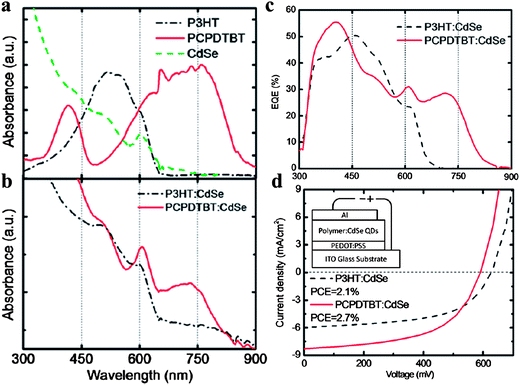 | ||
| Fig. 5 Comparison between P3HT:CdSe and PCPDTBT:CdSe blends. (a) Absorption spectra of P3HT, PCPDTBT, and CdSe films; (b) absorption spectra of P3HT:CdSe and PCPDTBT:CdSe films (87.5 wt% of NCs); (c) EQE spectra of P3HT:CdSe and PCPDTBT:CdSe devices, where the contribution from PCPDTBT is clearly observed; (d) J–V curves of the two devices under a solar simulator (AM 1.5 100 mW cm−2). Reproduced with permission from ref. 89, Copyright 2011, Elsevier. | ||
These problems could be partially solved by optical engineering. For example, Xue and co-workers attached a transparent hemispherical polymer microlens array (MLA) to the light incident surface of the device (see Fig. 6a for the scanning electron micrograph image of the MLA).93 As shown in Fig. 6b, with this array, light striking a microlens will be refracted into the active layer due to the curved shape of the microlens, which increases the optical path length of the device. In addition, light reflecting off one microlens could strike a neighboring one and contribute to the absorption, which reduces light reflection losses. With the MLA, they demonstrated that the device efficiency of PCPDTBT:CdSe blends could be increased by ∼30%.93 In addition, this MLA optical approach is not limited to hybrid PVs, and could also be applied to other polymer solar cells. The same group also employed an optical spacer to increase the optical absorption in the device.94Fig. 6c and 6d show a comparison of the calculated optical profiles between devices without (Fig. 6c) and with (Fig. 6d) an optical spacer (a layer of ZnO film).91 The inclusion of a ZnO layer results in optimized optical electric field distribution in the active layer, with significantly enhanced light absorption in the NIR regime. They fabricated devices and demonstrated that the optical spacer improved the short-circuit current, and hence the device efficiency, by nearly 30%. In addition to this optical contribution, this layer of ZnO might also work as an effective hole-blocking layer and an exciton dissociation site in the device, which collectively gave rise to this 30% improvement.
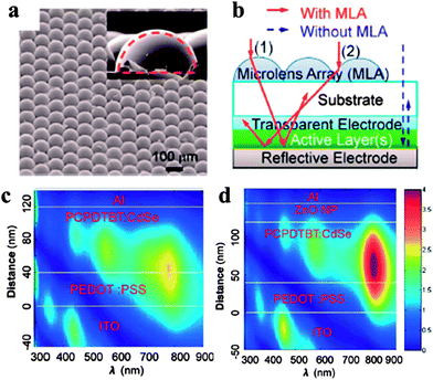 | ||
| Fig. 6 Demonstration of the effect of optical engineering on light absorption. (a) A scanning electron micrograph image of a representative microlens array (MLA); (b) schematic illustration of light behavior with (solid arrows) and without (dashed arrows) an MLA for an organic solar cell. With an MLA, the optical path length is increased and the light reflection loss is decreased; (c and d) calculated light intensity profiles for the devices without (c) and with (d) an optical spacer (a layer of ZnO film). With an optical spacer, the optical electric field is enhanced in the active layer. (a and b) Reproduced with permission from ref. 93, Copyright 2012, The Royal Society of Chemistry. (cand d) Reproduced with permission from ref. 91, Copyright 2012, The Royal Society of Chemistry. | ||
In addition, considering the fact that organic materials usually absorb light within a limited regime, two or more cells with complementary absorption regimes can be stacked together to maximize light absorption. The device with this structure is termed as a tandem cell, and has attracted much attention in polymer:fullerene blends.95,96 However, few reports on the tandem structure exist for hybrid PVs. Recently, Krebs and co-workers demonstrated a tandem cell based on polymer:ZnO blends.97 By using thermocleavable polymer materials, they successfully solved the solubility problem during deposition of subsequent layers in the stack, and extended the device absorption over a wide regime. Although the efficiency of their device was low, this work successfully demonstrated the possibility of fabricating hybrid PV-based tandem solar cells entirely by solution processing.
2.4 Exciton diffusion and dissociation in hybrid PVs
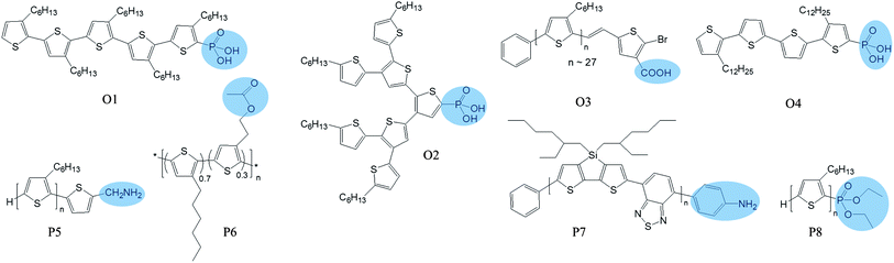
Upon photon absorption, strongly bound excitons are generated, with a binding energy around 0.4–0.5 eV.98,99 The excitons thermally diffuse into the BHJ interfaces, with a diffusion length around 5–15 nm and a lifetime on the order of nanoseconds,100–105 after which, they will recombine geminately. This means that donor and acceptor materials have to be well mixed to guarantee efficient exciton dissociation. However, a fine mixture will harm charge transport to the electrodes, increasing the opportunity for oppositely charged carriers to meet and recombine. As a result, a good balance has to be made to favor both charge separation and charge transport. We will discuss this morphology requirement in detail in Section 2.5.1.Once excitons arrive at the interfaces, the electrons might be transferred to the acceptor. There are two requirements for this charge transfer process to happen. (1) Since charge transfer is a short-range interaction that takes place when there is strong wave-function overlap between the donor and acceptor materials, the polymer and NCs must be in close contact with each other; (2) an energetic offset between the donor and acceptor LUMOs should be guaranteed so that the singlet exciton binding energy is overcome by this charge transfer process. For polymer:fullerene and polymer:polymer blends, condition (1) is usually well satisfied, and only condition (2) needs to be taken care of. However, for polymer:NC blends, bulky ligands like oleic acid (OA) or trioctylphosphine oxide (TOPO), necessary for NC synthesis, create a barrier for electron transfer between the polymer and NCs (see Fig. 7 for chemical structures of the ligands mentioned in this article). As a result, condition (1) becomes a serious problem in hybrid PVs. Intensive engineering work, including ligand treatments, polymer modification, and direct growth of NCs in polymers, has been devoted to the interface between polymers and NCs.
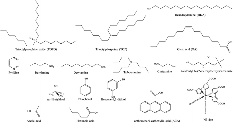 | ||
| Fig. 7 Chemical structures of the ligands discussed in this article. | ||
(a) Pyridine treatment of long ligands. Greenham et al. noticed that long ligands used in the NC synthesis were harmful to the charge transfer process between polymers and NCs.11 As a result, ligand exchange processes, where NCs covered with long synthesis ligands are treated with short ones, are needed to obtain good device performance. They investigated the PL quenching of MEH-PPV:NC blends, where either TOPO-coated or pyridine-treated NCs were used. With TOPO covered on the NC surface, no PL quenching was observed for MEH-PPV:CdS blends, indicating no electron transfer from MEH-PPV to CdS NCs. However, for the blends where the NC surface was treated with pyridine, there was significant quenching of PL, implying efficient electron transfer from the polymer to NCs. Different from the CdS case, substantial PL quenching was observed when TOPO-coated CdSe NCs were used. As there was a good overlap between the MEH-PPV emission spectrum and the CdSe NC absorption spectrum, this PL quenching could be explained by Förster resonance energy transfer (FRET). The FRET mechanism is based on a dipole–dipole interaction, and can be observed with a donor–acceptor distance of several nanometers.106 The PL quenching became enhanced after the ligand exchange process, demonstrating charge transfer from MEH-PPV to CdSe NCs.
This experiment by Greenham et al. showed that it is necessary to replace long ligands with short ones to ensure effective charge transfer between polymers and NCs. In addition, it also demonstrated that effective PL quenching does not necessarily mean efficient charge transfer, as energy transfer could be another route for PL quenching. Since then, ligand exchange using pyridine has been routinely used for hybrid PV fabrication. Later on, it was further demonstrated that this pyridine treatment method could also be applied to hybrid PVs based on nanorods and tetrapods.12,13 In 2003, the Alivisatos group investigated the issue of ligands and PL in more detail using P3HT:CdSe blends. They found that excess pyridine could be removed by pumping the device under low pressure (<10−6 mbar) and/or thermal annealing, due to the low boiling point of pyridine.107 The device performance could be significantly improved with the thermal annealing process.
As will be discussed later, pyridine treatment of NCs has been challenged recently, since devices based on NCs treated with other short ligands (like amines, thiols, or acids) have been reported to outperform those based on pyridine-treated NCs. However, more recently, Celik et al. demonstrated a high efficiency of 3.4%, where they used PCPDTBT and pyridine-treated CdSe nanorods.90 The key for this high efficiency was that the NCs were carefully washed in polar and non-polar solvents before ligand exchange. Based on transmission electron microscopy (TEM) and time-of-flight mass spectrometry measurements, they proposed that the washing process removed weakly bound bulky ligands and made the ligand exchange process more efficient.
(b) Amine treatment of long ligands. In 2005, Sargent and co-workers treated PbS NCs with octylamine, and blended NCs with MEH-PPV.39 Although the device efficiency was low, there was significant improvement compared with devices fabricated from OA-coated NCs, demonstrating the effectiveness of amine treatment. Later on, Carter and co-workers thoroughly investigated P3HT:CdSe blends with different short ligands on the NC surface, including tributylamine, butylamine, and pyridine.108 Their comparison concluded that devices based on butylamine-treated CdSe NCs gave the highest efficiency. Butylamine was also proved to be an effective surfactant for PbS NCs, with polymer:PbS blends demonstrating an efficiency of over 0.5%.41
In addition to these direct treatments of long ligands with short amines, Prasad and co-workers developed an indirect method to reach the aim.109 They replaced the bulky synthesis ligand with tert-butyl N-(2-mercaptoethyl)carbamate, which has a tert-butoxycarbonyl (tBOC) group. The tBOC group releases isobutene and carbon dioxide during thermal annealing, leaving cysteamine around the NC surface. Although the device fabricated from this indirect method did not show improvement in PCE compared with direct treatment, the authors suggested that this method led to facile multilayer fabrication, which was useful for tandem cells.
(c) Thiol treatment of long ligands. The development of colloidal quantum dot solar cells has benefitted a lot from thiol treatment, where a layer-by-layer (LBL) dip-coating process was employed for ligand exchange.110,111 The reason for using this LBL process was that NCs easily got aggregated when thiol-treatment was performed in solution.
Although the LBL process for ligand exchange has not been used to fabricate hybrid PVs, alternative approaches have been successfully employed to make use of thiols for hybrid PVs. For example, in 2008, Cao and co-workers managed to treat TiO2 NCs with thiophenol. They demonstrated that thiophenol-treated NCs quenched polymer PL more efficiently due to enhanced charge transfer.80 As a result, devices based on thiophenol-treated NCs showed improved performance compared with those treated with other ligands. Wu and Zhang managed to perform thiol treatment using a vapor annealing method.112 They spin-coated blends of P3HT and pyridine-treated CdSe NCs, after which the substrate was left for vapor annealing using benzene-1,3-dithiol at 120 °C. They employed nuclear magnetic resonance (NMR) and Fourier transform infrared spectroscopy (FT-IR) experiments to prove that benzene-1,3-dithiol diffused into the blend film and replaced some of the original ligands during the vapor annealing process. As a result, the short-circuit current and power conversion efficiency improved by ∼70% compared with the control device which was not vapor-annealed. This vapor annealing method was borrowed by Chou and co-workers.19 Combined with polymer and device structure engineering, they achieved a record efficiency of 3.2% for CdTe-based hybrid PVs. Alternatively, Prasad and co-workers employed a post-ligand exchange method to replace OA ligands with 1,2-ethanedithiol (EDT).20 They spin-coated blends of PDTPBT and OA-coated PbS NCs, after which EDT solution in acetonitrile was spin-coated on the blend film to exchange OA. With a layer of TiO2 NCs as the hole-blocking layer beneath the cathode, their device exhibited a high efficiency of 3.78%, significantly improved compared with previous PbS-based hybrid PVs.41 Almost published at the same time as Prasad's paper, Ren et al. reported a high efficiency of 4.1% for hybrid PVs based on P3HT and CdS NCs, which were also treated with EDT.16 The P3HT:CdS blend film, where CdS NCs were already treated with butylamine, was dipped in EDT solution in acetonitrile for 30 s and then left for solvent annealing overnight. The EDT-treated device showed ∼70% improvement in device efficiency compared with the non-treated one.
More recently, Brutchey and co-workers demonstrated that tert-butylthiol-treated CdSe NCs could easily be dissolved in tetramethylurea at concentrations up to 100 mg ml−1. They blended P3HT with tert-butylthiol-treated CdSe nanodots and obtained an efficiency of 1.9% without any thermal annealing process.113 They emphasized that the thiol provides stronger binding with CdSe NCs compared with an amine or pyridine.113,114 As a result, the ligand exchange efficiency using thiol is higher, thereby improving charge transfer. In addition, they also found that the LUMO and HOMO levels of NCs changed with different ligand treatments. The open-circuit voltage increased to 0.8 V due to a favorable band alignment between the P3HT HOMO and the CdSe LUMO in the tert-butylthiol-treated case.
(d) Acid treatment of long ligands. The bulky synthesis ligand on the NC surface could also be replaced by an acid. Similar to their approach for exchanging long ligands with thiol,20 Prasad and co-workers used a post-chemical treatment to exchange long ligands with the acid.115 The film, spin-coated from a solution made of P3HT and OA-capped PbS NCs, was immersed into an acetic acid solution for 30 min for ligand exchange. They used PL decay to confirm that the charge transfer was enhanced for the acid-treated film. As a result, this post-chemical treatment resulted in a significant improvement of the device performance.
An alternative approach is to perform acid treatment before spin-coating, which was developed by Krüger and co-workers and proved to be a great success.15 The CdSe NCs covered with a long synthesis ligand, hexadecylamine (HDA), were washed using hexanoic acid (HA). The authors proposed that this acid treatment process resulted in the formation of an organic salt, effectively removing the ligand HDA (see Fig. 8). The resulting organic salt was easily separated from the NCs by centrifugation. They blended P3HT with the acid-treated CdSe nanodots, and obtained a power conversion efficiency of 2%, which was the highest efficiency for devices based on CdSe nanodots at that time.15 Later on, they found that this acid treatment method could also be applied to CdSe NCs covered with TOP/OA ligands.89 This experiment demonstrated the generality of the acid treatment method. However, considering that it is difficult to figure out a reaction between TOP/OA and HA to remove the TOP/OA ligands, more experiments are needed to understand the exact mechanism of this promising acid treatment method. It might be possible that this acid-treatment method is a normal ligand-exchange process, rather than a chemical reaction.
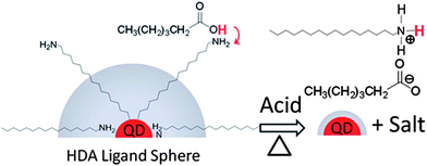 | ||
| Fig. 8 Schematic illustration of the proposed mechanism for the acid treatment process. Hexanoic acid forms an organic salt with the synthesis ligand (hexadecylamine), effectively reducing the size of the insulating organic layer on the NC surface. Reproduced with permission from ref. 15, Copyright 2010, American Institute of Physics. | ||
In addition to these short insulating acid ligands, Chen, Su, and co-workers demonstrated that a conductive acid could also be used to enhance the charge transfer between the polymer and NCs.81 They made devices using P3HT and TiO2 nanorods, which were treated with anthracene-9-carboxylic acid (ACA). The ACA molecule consists of an anthracene moiety that is conductive, and has a strong binding energy with TiO2. From the PL lifetime measurement, the authors found that the blends based on ACA-treated NCs showed shorter time than those based on pyridine-treated or OA-capped NCs, demonstrating enhanced charge transfer between P3HT and TiO2 NCs. Indeed, with ACA treatment, the device showed much improved performance.
Later on, the same group further extended this idea, and they used dyes which contained acid groups as the ligand molecules (N3-dye, see Fig. 7 for the chemical structure).82 The employment of dyes in their experiments made the devices function similar to solid state dye-sensitized solar cells, where dyes absorb light and transfer charges to charge-conducting materials. However, the authors claimed that the dyes in their experiments served to help charge transfer (rather than absorb light), which was supported by the fact that there was no contribution from the dye absorption regime in the EQE spectrum. They used PL quenching and PL decay experiments to demonstrate that the N3-dye helped in enhancing charge transfer, and hence increased the photocurrent. In addition, they also showed that these 3D bulky dye ligands could help in slowing down back recombination, which 'increased both the open-circuit voltage and the photocurrent.
(e) Ligand treatment efficiency. An interesting result raised in the above mentioned Krüger's paper is that NMR experiments revealed the presence of the synthesis ligand HDA after acid treatment.15 Unfortunately, they did not further explore the effect of the residual HDA ligand on their device performance, possibly due to the difficulty to quantify the amount of remaining ligand. Anyhow, this information triggered a fundamental question: what is the efficiency of these ligand treatment methods?
As early as the 1990s, Alivisatos' group and Bawendi's group proved that the ligand exchange of TOPO with pyridine was not complete.116,117 Using NMR and thermal gravimetric analysis, Bawendi and co-workers demonstrated that after ligand exchange, around 90% of the NC surface was covered with ligands, 10–15% of which was the long synthesis ligand TOPO.117 Considering that only 30% of the NC surface was covered with TOPO before ligand exchange, the ligand exchange efficiency was around 60%. In addition, this value is expected to change with the size and shape of NCs.116 Holt et al. investigated ligand exchange efficiency by employing FT-IR techniques, and they found that an amine, thiol or acid was not able to completely replace TOPO.118 There are also other reports which provided evidence for incomplete exchange of OA using pyridine or an amine.119,120 Therefore, it seems that most short ligands cannot completely replace the long synthesis ligands during the ligand exchange process.
By collaborating with Krüger's group, Meerholz and co-workers further confirmed that ligand treatment is incomplete using a physical method.121 Different from previous approaches, where experiments were performed on pure NCs, their experiments were performed on polymer:NC blends after thermal annealing, making their results more relevant to final devices. They employed spectroscopic ellipsometry and transmission intensity data to determine the volume ratios between polymers and NCs in polymer:NC blends, where an effective medium approximation based on single-component films was applied. As shown in Fig. 9, the volume ratios (Vpolymer/VNC) in both blends (P3HT with either pyridine-treated or acid-treated CdSe nanodots) were significantly smaller than in the ideal case, where no ligands were assumed on the NC surface. This result implied that there were ligands remaining on the NC surface. These ligands increased the NC volume, and hence decreased the volume ratio between the polymer and NCs. Based on some reasonable assumptions on the blend configurations, they further calculated that the ligand layer thickness was ∼0.9 nm for pyridine-treated NCs and ∼0.6 nm for acid-treated ones. The calculated organic layers were thicker than the molecular size of pyridine or HA, which confirmed that the ligand treatment was not complete.121
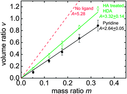 | ||
| Fig. 9 Volume ratios (v = Vpolymer/VNC) as a function of mass ratios (m = Mpolymer/MNC) for P3HT:CdSe blends, with pyridine-treated (circles) and acid-treated (squares) NCs, where A = v/m. The dashed line indicates the ideal case where P3HT is blended with uncoated CdSe NCs. The decreased volume ratio compared with the ideal case indicates remaining ligands on the NC surface. Data taken from ref. 121. | ||
Considering incomplete ligand exchange, it might be beneficial to have a thorough investigation of the effect of different ligands (including pyridine, amine, thiol, and acid) on the charge transfer process between the polymer and NCs. Different ligands have different binding affinities with NCs, and hence different abilities to replace the original bulky ligands, which affect the charge transfer process. In addition, different ligands might bring or remove different amounts of trap sites, which will affect charge transport and charge recombination (Section 2.5.3). It is desirable to pick up a few ligands which best suit charge transfer and charge transport processes.
 | ||
| Fig. 10 Chemical structures of the polymers and oligomers with functional groups which help them to attach to NCs. The functional groups are illustrated in shadow. | ||
In 2003, Alivisatos, Fréchet, and co-workers added phosphonic acid binding groups to oligothiophenes (O1 in Fig. 10), which were then used as ligands for CdSe NCs.122 They demonstrated that the oligomers with five or more thiophene rings underwent charge transfer with CdSe NCs. Although they did not measure the photovoltaic effect of these oligothiophene:CdSe complexes, they proposed that these complexes could work as solar cells by themselves. In addition, they also proposed that that these modified oligothiophenes could be used as a third component in a polymer:NC blend to enhance electronic coupling between polymers and NCs. Indeed, one year later, Locklin et al. employed a similar strategy and added phosphonic acid binding groups to conjugated oligothiophene dendrons (O2 in Fig. 10).123 They demonstrated that these dendron:NC complexes worked as solar cells on their own, with 0.29% power conversion efficiency under 0.14 mW cm−2 illumination. The other idea proposed by Alivisatos to use these modified oligomers as a third component to mediate the interaction between polymers and NCs was also realized recently. Chen, Su, and co-workers synthesized a bromine-terminated thiophene oligomer (O3 in Fig. 10), which was used to enhance electronic coupling between P3HT and TiO2 NCs. Improved device performance was observed for P3HT:TiO2 blends with this third component.124
Alivisatos and co-workers also employed this strategy in polymers. They added amino groups to polythiophene (P5 in Fig. 10) to increase the miscibility between polymers and NCs.125 When blended with CdSe NCs, the modified polythiophene showed improved performance compared with the control polymer. Based on TEM images, they believed that the performance improvement was due to enhanced intimacy and improved morphology. Janssen and co-workers confirmed this intimacy induced by the polymer functional groups using electron tomography.126 Electron tomography makes it possible to reconstruct the 3D networks of the active layer, providing critical morphological parameters that are valuable for improving the device performance.127 They added ester groups to polythiophene (P6 in Fig. 10) as the donor and used ZnO NCs as the acceptor. Using electron tomography, they could visualize the effect of the ester groups on the intermixing of the two materials in 3D. As shown in Fig. 11, the images clearly confirm that ZnO NCs disperse much better in P6 than in the control polymer, P3HT. Their photo-induced absorption experiments revealed that this intimacy enhanced charge transfer, and hence charge generation for the P6:NC blends. Recently, this functional group approach was also used to fabricate highly efficient CdTe-based hybrid OPVs, where aniline groups on the polymer (P7 in Fig. 10) served as a strong anchor to attach to CdTe NCs.19
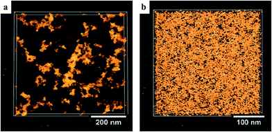 | ||
| Fig. 11 Reconstructed volumes from electron tomography for (a) P3HT:ZnO and (b) P6:ZnO. ZnO appears yellow, and the polymer looks transparent against a black background. It is clear that amino groups in P6 help NCs disperse much better in the polymer matrix. Reproduced with permission from ref. 126, Copyright 2011, WILEY-VCH Verlag GmbH & Co. KGaA, Weinheim. | ||
These functional groups were also used to fabricate hybrid OPVs made of single nanowires by Yang, Fréchet, and co-workers (see Fig. 12 for device structure).128 End-functionalized oligo- or poly-thiophene (O4 and P8 in Fig. 10) was grafted onto ZnO nanowires. This single core–shell nanowire (ZnO core and thiophene shell) demonstrated photovoltaic behavior, indicating efficient charge generation and transport.
The in situ NC formation approach was initiated by Janssen's group.78 They prepared blends of MDMO-PPV and a titanium precursor. The titanium precursor formed TiO2 within the polymer matrix via hydrolysis in air. The authors confirmed charge transfer from the polymer to TiO2 using PIA experiments. The devices demonstrated photovoltaic response, with a peak EQE around 11%. By optimizing the ratio between the polymer and TiO2, they improved the power conversion efficiency to ∼0.2%.79 The relatively low efficiency of the device was limited by the amorphous nature of TiO2. Although crystallization of TiO2 could be achieved by annealing the film at temperatures over 350 °C, high temperatures will destroy the polymer. To overcome this problem, they switched to the ZnO precursor, considering that ZnO could crystallize at low temperatures. By annealing a solution containing MDMO-PPV and a ZnO precursor at 110 °C, they obtained devices with a PCE of over 1%, which was improved compared to the TiO2 case.75
However, Blom and co-workers noticed that MDMO-PPV degraded in the presence of a TiO2 precursor (diethylzinc).129 Based on UV-vis spectroscopy and charge-transport studies, they proposed that trans vinyl bonds in the PPV backbone broke and converted to a non-conjugated species, which limited the device performance. They avoided this degradation by using P3HT, which does not contain vinyl moieties and is more stable than MDMO-PPV. The devices based on P3HT showed a power conversion efficiency of 1.4%, higher than the MDMO-PPV case. By optimizing the active layer thickness, Janssen and co-workers further improved the efficiency to 2%, which is the record efficiency for ZnO-based hybrid PVs currently.76 Aided by electron tomography, they identified that the relatively poor efficiency of thin devices was related to low charge carrier generation as well as exciton quenching at the electrodes. For thicker devices, the device performance was improved as a result of favorable phase separation, although increasing thickness resulted in difficulties to collect charge carriers.
In addition to metal oxides, in situ formation was also successfully employed to prepare metal chalcogenides. The growth of lead chalcogenide in a polymer matrix was first reported by Watt et al.130,131 Although the photovoltaic effect was not measured in their initial reports, they used PL quenching experiments to demonstrate charge transfer between polymers and NCs. In a following study, they reported a power conversion efficiency of 0.7% for devices based on PbS NCs synthesized in MEH-PPV.40 A considerable improvement in device efficiency was made by Liao et al., who made use of the P3HT chain as a template to synthesize CdS nanorods and obtained a PCE of 2.9% (see Fig. 13 for the synthesis mechanism).70 The aspect ratio of CdS nanorods could be controlled by varying the cosolvent ratio during synthesis. Their results also demonstrated enhanced PL quenching and improved performance with increasing NC aspect ratio.
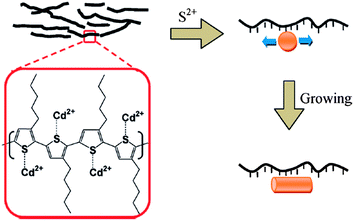 | ||
| Fig. 13 Schematic illustration of in situ growth of CdS nanorods in the P3HT matrix. Cd ions in the cadmium precursor couples with unpaired S atoms along the P3HT chain. Following addition of the sulfur precursor, CdSe starts to nucleate and grows along the P3HT chain, forming nanorods. Reproduced with permission from ref. 70, Copyright 2009, American Chemical Society. | ||
Note that there is difference between the synthesis method used by Watt or Liao and that by Janssen or Blom. For the former, the NCs were already formed before spin-coating the film, while for the latter, NCs were formed by decomposition of the precursor during and after the deposition process. In principle, the latter method is more convenient because it does not require a NC synthesis process before film deposition. Recently, Haque and co-workers reported P3HT:CdS devices fabricated from thermal decomposition of a cadmium xanthate precursor in a P3HT film.132 The key point in this work was that only volatile decomposition products were produced so that no by-products were left in the final device. Using transient absorption, they demonstrated that their films exhibited the generation of long-lived charges, indicating efficient charge transfer. The PCE of the initial device was 0.72%, which was increased to 2.17% by optimizing the thermal annealing temperature of the composite film.133 They also applied this method to the fabrication of polymer:CuInS2 devices, and obtained a high efficiency of 2.8%,21 which is much improved compared with the previous work based on CuInS2 NCs.67
2.5 Charge transport and collection
After exciton dissociation, holes are left on the donor phase and electrons are transferred to the acceptor phase. For polymer:fullerene and polymer:polymer blends, due to weak screening of the electric field, a strong coulombic attraction still exists for these electron–hole pairs (known as charge-transfer states).134 The charge-transfer states could decay geminately, being a loss to the photocurrent. However, this geminate decay of charge-transfer states is less likely to occur for hybrid PVs, considering the large dielectric constant of inorganic NCs. In other words, the electron and hole dissociated from an exciton are relatively free from each other. Indeed, recent transient absorption measurements indicated that polarons barely decayed between 1 and 100 ns for devices based on P3HT and CdSe nanodots.135 This means that geminate loss is not a dominant loss mechanism for hybrid PVs.These free charges have to be transported to the electrodes, so that they can contribute to the photocurrent. Ideally, a highway is needed for electrons and holes to their respective electrodes. However, in a BHJ structure, it is difficult to guarantee such a percolation path. As a result, the charge transport to the electrodes could be severely hindered by parameters like morphology, mobility, and traps, which have to be optimized.
Alivisatos and co-workers have shown that the solvent had a significant effect on the film morphology, and hence the device efficiency.107 A two solvent mixture approach, where one was a good solvent for NCs and the other was a good solvent for the polymer, was used to control the morphology down to the nanometer scale. As shown in Fig. 14a, by optimizing the volume ratio between chloroform (a good solvent for the polymer) and pyridine (a good solvent for NCs), they could increase the EQE value by a factor of 1.4. They further demonstrated that this optimized volume ratio was dependent on the shape and size of NCs, as a result of different non-passivated Cd surface sites on different samples. In addition to the ratio between mixed solvents, Sun, Greenham, and co-workers demonstrated that choosing an appropriate solvent for the polymer was also crucial for the film morphology.136 They investigated the effect of different solvents on the performance of devices based on MDMO-PPV and CdSe tetrapods. As shown in Fig. 14b, they found that a high boiling point solvent (1,2,4-trichlorobenzene) resulted in much improved efficiency compared with a low boiling point solvent (chloroform). They proposed that slow evaporation of the high boiling point solvent gave rise to favorable phase separation between the polymer and NCs, which was beneficial to charge transport.
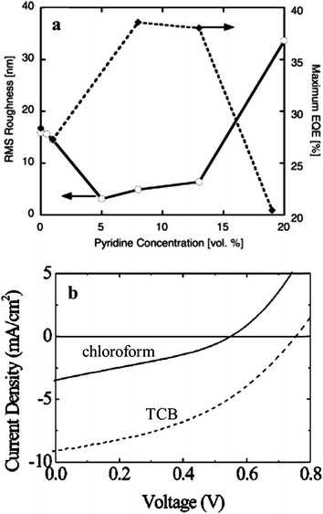 | ||
| Fig. 14 The effect of solvents on the film morphology and device performance. (a) The device EQE value could be maximized by controlling the volume ratio in binary solvent blends, where the active layer was composed of P3HT and CdSe nanorods; (b) different solvents (TCB is short for 1,2,4-trichlorobenzene) for the polymer resulted in different J–V curves (one sun conditions) for blends of MDMO-PPV and CdSe tetrapods, demonstrating the importance of choosing an appropriate solvent for the polymer. (a) Reproduced with permission from ref. 107, Copyright 2003, WILEY-VCH Verlag GmbH & Co. KGaA, Weinheim. (b) Reproduced with permission from ref. 136, Copyright 2004, American Institute of Physics. | ||
Janssen and co-workers employed electron tomography to investigate the effect of thickness on the film morphology, where ZnO NCs were in situ formed in the P3HT matrix.76 The authors found considerable difference between films with different thicknesses. The thin film showed very large polymer domains, with the domain size significantly larger than the exciton diffusion length. With increasing film thickness, they observed finer phase separation between the donor and the acceptor. As we said before, large phase separation benefits charge transport while small phase separation benefits exciton dissociation. This experiment by Janssen's group demonstrated that a balance had to be reached between these two processes in order to maximize the device performance. They found that the optimized thickness for their device was ∼225 nm, above which the disadvantage of transporting charge carriers outweighed the advantage of generating more charges. As discussed in Section 2.4.2, the same group also used electron tomography to investigate the effect of polymer functional groups on the film morphology (see Fig. 11).126 Consistent with this thickness-dependence work, although polymer functional groups enhanced the intimacy between the polymer and NCs, and hence improved exciton dissociation, this intimacy was detrimental for thick devices as it hindered charge transport.
Inspired by this idea, much engineering work has been devoted to improving the transport between NCs. A significant improvement was made by Alivisatos and co-workers, who replaced nanodots with nanorods and obtained a PCE of 1.7%.12 The idea behind it was that nanorods reduced the number of interparticle hops required, providing a direct path for electron transport. The authors demonstrated that the EQE value not only increased from nanodots to nanorods, but also increased with increasing nanorod length. It would be ideal if nanorods could stand perpendicular to the substrate so that the electrons could be collected by the electrode within only a few hops. However, cross-section TEM images revealed that nanorods tended to lie in the plane of the film, rather than perpendicular to the film.12 Recently, Greenham and co-workers further confirmed this parallel alignment using electron tomography, where they could even quantify that around 80% of the nanorods were within 10° of parallel alignment.138 They also identified that ∼10% of the nanorods could not find their pathway to the electrode, serving as morphological traps for electrons.
Considering these disadvantages of the nanorods, tetrapods, whose shape made it impossible for them to lie in the plane of the film, were explored as the acceptor.13 Sun, Greenham, and co-workers demonstrated that the devices made with tetrapods showed improved performance compared with those made with nanorods, where MDMO-PPV was used as the donor.13 Since then, the tetrapod shape has become the key for achieving high efficiency in hybrid PVs.18,19 A comparison between electron transport in NCs with different shapes is schematically illustrated in Fig. 15. In addition, Alivisatos and co-workers tried an even more complex shape, i.e. a hyperbranched structure, aiming at further improving the charge transport.14 Unfortunately, the devices made from this hyperbranched structure were limited by the fact that the polymer was not able to fully penetrate NC branches.
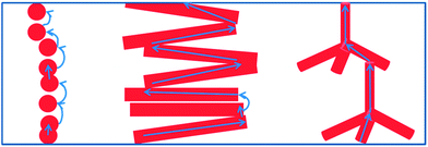 | ||
| Fig. 15 Schematic illustration of electron transport in NCs with different shapes. Interparticle hops are illustrated using curved lines, while direct transport is illustrated using straight lines. | ||
Although the strategy of using tetrapods proved to be successful in improving the device performance, recent literature indicated that it might be beneficial to go back towards nanorods or even nanodots. It was demonstrated by two independent papers that a blend of nanodots and nanorods could help in improving charge transport over pure nanodots or nanorods.140,141 One of the papers suggested that the insertion of nanodots into nanorods could help in reducing the horizontal aggregation of nanorods, resulting in an increased tendency for nanorods to lie perpendicular to the film and hence improved transport.140 Another study proposed that the addition of nanodots into nanorods simply filled the gaps between nanorods, improving transport.141 Although the exact mechanism needs to be further verified, e.g. using electron tomography, it seemed that the blend of nanorods and nanodots indeed improved the efficiency over pure nanodots or pure nanorods.140,141 By optimizing the ratio between nanodots and nanorods, a high efficiency of 3.5% could be obtained for the devices based on this nanorod–nanodot blend and PCPDTBT.141 In addition, it was also demonstrated that increased efficiency could be obtained by simply increasing the NC size.135,140,142 By using acid-treated large NCs (7.1 nm) and PCPDTBT, Krüger and co-workers demonstrated a high efficiency of 3.1%,140 which was comparable to that based on tetrapods.18 However, more experiments might be needed to understand the physics behind the efficiency improvement with increasing NC size and further explore the potential of this promising approach.135
In addition to shape engineering, another method to optimize the electron mobility is to engineer ligands on the NC surface. The ligand treatment method discussed in Section 2.4.1 not only helps in enhancing the intimacy between polymers and NCs, enhancing charge separation, but also helps in improving the electron mobility, enhancing charge transport. The short or conductive ligands on the NC surface make the electron transport easier by improving the electric coupling between NCs. For example, Ren et al. demonstrated the effect of EDT treatment on charge transport properties by measuring the J–V curves of electron-only devices.16 It was found that the devices treated with EDT showed a strong enhancement of electron transport over the untreated ones. Lefrançois et al. investigated the effect of different ligands on charge transport in detail.143 They measured the J–V curves of CdSe films treated with a range of different ligands. As shown in Fig. 16, all the films after ligand treatment showed improved charge transport, which was attributed to a decreased interparticle distance after treatment. The effect of EDT treatment was the most significant, with an improvement by approximately five orders of magnitude in conductivity. The authors ascribed this significant improvement to the short size of the EDT molecule, strong interaction between the thiolate and NCs, as well as relatively easy ligand exchange for aliphatic ligands compared with arylene ones.143 This experiment was performed on pure NC films, rather than polymer:NC blend films. However, it demonstrated the importance of choosing appropriate ligands to optimize the electron transport.
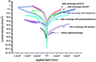 | ||
| Fig. 16 The effect of different ligands on charge transport of CdSe films, demonstrating the importance of choosing an appropriate ligand for transport optimization. Reproduced with permission from ref. 143, Copyright 2011, The Royal Society of Chemistry. | ||
Although much attention has been focused on improving the electron transport, in principle, the hole transport is of equal importance. P3HT could form fibril structures under certain processing conditions, with good π–π stacking along the fibril and improved mobility.144 Sun and Greenham made use of this, and demonstrated that by using a high boiling point solvent to induce the P3HT fibril formation, the P3HT:CdSe device efficiency could be increased by a factor of around 50%.17 A similar strategy was also employed by Ren et al. to improve the performance of P3HT:CdS devices.16
Actually, in the original paper by Greenham et al., the effect of traps on the device has been mentioned.11 They observed that at intensities up to 10 W m−2, the short-circuit current was approximately linear with the illumination intensity. The linear dependence of current on light intensity is characteristic of recombination at a fixed number of recombination sites, consistent with recombination mediated by trap states.
Another technique to investigate traps is PIA spectroscopy. In Section 2.3.1, we have discussed PIA as a useful tool to qualitatively examine whether long-lived charge carriers are generated in a system. Actually, PIA could also help in obtaining information on the lifetime distribution and recombination dynamics of these charge carriers by varying the excitation frequency. If lifetimes of charge carriers exceed the inverse of excitation frequency, their absorption will be suppressed in the PIA signal. Using this technique, Ginger and Greenham found that the lifetime of charge carriers spanned a wide range from less than 100 μs to more than several ms for MEH-PPV:CdSe blends.145 The lifetime exceeding several ms was consistent with the presence of trapped charge carriers, which resulted in slow recombination and long lifetime. Similar wide distribution of lifetimes was also reported for P3:CdSe blends.87 The authors found that a model for dispersive recombination, which accounted for the effects of traps, had to be employed to fit their data. Using the same technique, Heinemann et al. compared the recombination for P3HT:PCBM and P3HT:CdSe blends. They also found that the model for dispersive recombination had to be used for fitting the P3HT:CdSe data, while a bimolecular recombination could fit the P3HT:PCBM data well. This further confirmed significant effects of traps on the operation of hybrid PVs.146 In addition, transient absorption spectroscopy, a technique similar to PIA but extending to short time regimes, was also employed to demonstrate the presence of considerable trap states in hybrid PVs.135,147–149
In addition to PIA spectroscopy, Heinemann et al. used another technique, electron spin resonance (ESR), to further compare the difference between P3HT:PCBM and P3HT:CdSe and demonstrate the effects of traps on hybrid PVs.146 ESR is a useful technique to detect states with a non-zero spin, such as polarons or triplet excitons. By comparing the ESR signal before and after light excitation of the sample, it is possible to examine whether successful charge separation occurs in PVs. In addition, by observing the decay of light-induced ESR signals after switching off the light excitation, it is possible to examine the recombination dynamics of these light-induced charge carriers. As shown in Fig. 17, after light excitation, both P3HT:PCBM and P3HT:CdSe samples showed increased ESR signals, indicating successful charge transfer for both cases. For P3HT:PCBM, a rapid decay of the ESR signal was observed upon turning off the light excitation, indicating fast recombination of the generated charge carriers. In contrast, P3HT:CdSe showed complex decay dynamics, which was a superposition of a prompt decay in the subsecond regime and a persistent decay in the hour regime. The fast decay could be explained by bimolecular recombination between free charge carriers. The remaining charge carriers are deeply trapped, resulting in slow recombination and persistent decay.
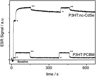 | ||
| Fig. 17 Temporal evolution of ESR signals, where the start of light excitation is marked as * and the termination of light excitation is marked as **. In contrast to the fast decay of P3HT:PCBM blends, P3HT:CdSe exhibits persistent decay, suggesting the presence of deep traps. Reproduced with permission from ref. 146, Copyright 2009, WILEY-VCH Verlag GmbH & Co. KGaA, Weinheim. | ||
Recently, Greenham and co-workers used transient photocurrent and photovoltage measurements to investigate the trap effects in hybrid PVs.135,150 Transient photocurrent measurements examine how the photocurrent responds to pulsed light illumination, providing useful information on charge transport, recombination and lifetime. Examining the light-intensity dependence of photocurrent response helps in revealing information on non-linear processes such as trapping and detrapping. Similar to PIA and ESR measurements, transient photocurrent measurements focus on long-lived species, suitable for investigating trapping effects. Fig. 18 compares transient photocurrent data for P3HT:PCBM and P3HT:CdSe devices under different light intensities. For P3HT:PCBM devices, fast turn-on and turn-off dynamics were observed under all the intensities investigated (Fig. 18a), with little change in the shape of curves (Fig. 18b), which was consistent with a relatively trap-free transport. In contrast, for P3HT:CdSe devices, both turn-on and turn-off dynamics were composed of fast and slow components (Fig. 18c and d). The slow components could be explained by the presence of a large amount of trap states. With increasing light intensity, an increasing amount of trap states was filled, which reduced the time to reach the steady state. Further examination of the transient photocurrents at different biases revealed that trapping effects were getting increasingly severe approaching the open-circuit voltage, maybe due to the field-dependent detrapping rate. The authors also examined the trapping effects using transient photovoltage measurements.150 Transient photovoltage measurements examine the voltage decay after a small perturbative light pulse for a device working under open circuit conditions. It is a direct measure of charge recombination kinetics under open-circuit conditions. The photovoltage measurements further demonstrated that the extraction of trapped charges was a limiting process for P3HT:CdSe devices.
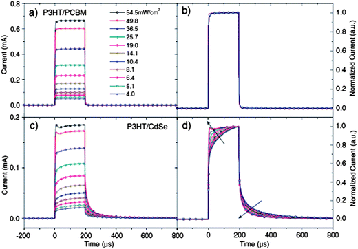 | ||
| Fig. 18 Transient short-circuit photocurrent for P3HT:PCBM blends (a and b) and P3HT:CdSe blends (c and d) at various intensities. (a and c) show the raw data, and (b and d) present normalized curves. Compared with P3HT:PCBM, the slow rise and decay of P3HT:CdSe indicate the presence of a large amount of charge traps. Reproduced with permission from ref. 150, Copyright 2011, WILEY-VCH Verlag GmbH & Co. KGaA, Weinheim. | ||
Though qualitative, all the above techniques revealed the detrimental effects of traps on the performance of hybrid PVs, particularly by comparing the behaviors between polymer:PCBM and polymer:NC devices. Further investigation is needed to help us further understand the trapping effects and improve the performance of hybrid PVs.
3 Conclusions and outlook
Although there was a bottleneck for the development of hybrid PVs with the efficiency saturating at ∼3% for a long time,31 these two years have witnessed the renaissance of this area. Power conversion efficiency exceeding 4% has been reported. In addition to CdSe, devices based on other NCs, including CdS, CdTe, PbS, TiO2, and CuInS2, also demonstrated promising efficiencies. These processes are encouraging, particularly considering that much fewer groups are working on polymer:NC blends than polymer:fullerene blends.Compared with polymer:fullerene devices, the polymer:NC devices seem to be limited by charge transfer and charge transport. In this sense, the ligands on the NC surface play a significant role in determining the device efficiency, since they affect both charge transfer and charge transport processes. In spite of the recent success in exploring alternative ligands to pyridine, more experiments are needed to understand how these ligands affect the polymer:NC interaction as well as the interaction between NCs. In addition, the effects of ligands on surface traps have to be investigated in more detail, so that recombination through trap states could be minimized.151 Alternative approaches, like direct growth of NCs in a polymer matrix, might also deserve further attention, due to their obvious advantages of bypassing ligand problems and their recent success in fabricating highly efficient devices. Another issue which deserves further attention is the film morphology, which is also closely related to both charge separation and charge transport. Electron tomography offers a powerful tool to examine different morphologies fabricated from different solvents and different NC shapes. It will be particularly interesting to investigate whether large nanodots are enough to improve the morphology and provide necessary percolation for charges, as suggested by some recent studies.
With the problems related to charge transfer and charge transport solved, it might be possible that polymer:NC blends would outperform polymer:fullerene blends, considering the advantages of NCs, like high dielectric constant and better absorption. As such, now it seems to be an appropriate time to consider the sustainability of hybrid solar cells concerning future large-scale applications. Fortunately, some research groups have started to use earth-abundant and environmentally benign materials (e.g. FeS2, Cu2S, CuO, Cu2ZnSnS4, CuInSe2, and CuInS2)21,66,152,153 to replace heavy metal-based NCs. This is of great importance for practical long-term development of this technology.
Acknowledgements
F. G. and J. W. thank Prof. Neil C. Greenham (University of Cambridge) for helpful discussions on hybrid PVs. S.R. thanks the financial support from the National Science Foundation under Award No. EPS-0903806 and matching support from the State of Kansas through the Kansas Board of Regents, University of Kansas New Faculty General Research Fund and Department of Energy-Basic Energy Sciences grant DESC0005448 for funding.References
- B. O'Regan and M. Gratzel, Nature, 1991, 353, 737–740 CrossRef CAS.
- C. W. Tang, Appl. Phys. Lett., 1986, 48, 183 CrossRef CAS.
- J. J. M. Halls, C. A. Walsh, N. C. Greenham, E. A. Marseglia, R. H. Friend, S. C. Moratti and A. B. Holmes, Nature, 1995, 376, 498–500 CrossRef CAS.
- G. Yu, J. Gao, J. C. Hummelen, F. Wudl and A. J. Heeger, Science, 1995, 270, 1789–1791 CAS.
- G. Li, R. Zhu and Y. Yang, Nat. Photonics, 2012, 6, 153–161 CrossRef CAS.
- Y. Yao, C. Shi, G. Li, V. Shrotriya, Q. Pei and Y. Yang, Appl. Phys. Lett., 2006, 89, 153507 CrossRef.
- C. R. McNeill, S. Westenhoff, C. Groves, R. H. Friend and N. C. Greenham, J. Phys. Chem. C, 2007, 111, 19153–19160 CAS.
- C. Groves, J. C. Blakesley and N. C. Greenham, Nano Lett., 2010, 10, 1063–1069 CrossRef CAS.
- C. R. McNeill and N. C. Greenham, Adv. Mater., 2009, 21, 3840–3850 CrossRef CAS.
- P. Guyot-Sionnest and M. A. Hines, Appl. Phys. Lett., 1998, 72, 686–688 CrossRef CAS.
- N. C. Greenham, X. Peng and A. P. Alivisatos, Phys. Rev. B: Condens. Matter Mater. Phys., 1996, 54, 17628–17637 CrossRef CAS.
- W. U. Huynh, J. J. Dittmer and A. P. Alivisatos, Science, 2002, 295, 2425–2427 CrossRef CAS.
- B. Sun, E. Marx and N. C. Greenham, Nano Lett., 2003, 3, 961–963 CrossRef CAS.
- I. Gur, N. A. Fromer, C.-P. Chen, A. G. Kanaras and A. P. Alivisatos, Nano Lett., 2007, 7, 409–414 CrossRef CAS.
- Y. Zhou, F. S. Riehle, Y. Yuan, H.-F. Schleiermacher, M. Niggemann, G. A. Urban and M. Kruüger, Appl. Phys. Lett., 2010, 96, 013304 CrossRef.
- S. Ren, L.-Y. Chang, S.-K. Lim, J. Zhao, M. Smith, N. Zhao, V. Bulović, M. Bawendi and S. Gradečak, Nano Lett., 2011, 11, 3998–4002 CrossRef CAS.
- B. Sun and N. C. Greenham, Phys. Chem. Chem. Phys., 2006, 8, 3557–3560 RSC.
- S. Dayal, N. Kopidakis, D. C. Olson, D. S. Ginley and G. Rumbles, Nano Lett., 2010, 10, 239–242 CrossRef CAS.
- H.-C. Chen, C.-W. Lai, I.-C. Wu, H.-R. Pan, I.-W. P. Chen, Y.-K. Peng, C.-L. Liu, C.-H. Chen and P.-T. Chou, Adv. Mater., 2011, 23, 5451–5455 CrossRef CAS.
- J. Seo, M. J. Cho, D. Lee, A. N. Cartwright and P. N. Prasad, Adv. Mater., 2011, 23, 3984–3988 CrossRef CAS.
- T. Rath, M. Edler, W. Haas, A. Fischereder, S. Moscher, A. Schenk, R. Trattnig, M. Sezen, G. Mauthner, A. Pein, D. Meischler, K. Bartl, R. Saf, N. Bansal, S. A. Haque, F. Hofer, E. J. W. List and G. Trimmel, Adv. Energy Mater., 2011, 1, 1046–1050 CrossRef CAS.
- J. Bouclé and J. Ackermann, Polym. Int., 2012, 61, 355–373 CrossRef.
- T. Song, S.-T. Lee and B. Sun, J. Mater. Chem., 2012, 22, 4216–4232 RSC.
- T. J. Bukowski and J. H. Simmons, Crit. Rev. Solid State Mater. Sci., 2002, 27, 119–142 CrossRef CAS.
- A. M. Smith and S. Nie, Acc. Chem. Res., 2010, 43, 190–200 CrossRef CAS.
- S. Kumar and T. Nann, J. Mater. Res., 2004, 19, 1990–1994 CrossRef CAS.
- S. A. McDonald, G. Konstantatos, S. Zhang, P. W. Cyr, E. J. D. Klem, L. Levina and E. H. Sargent, Nature Mater., 2005, 4, 138–142 CrossRef CAS.
- D. Cui, J. Xu, T. Zhu, G. Paradee, S. Ashok and M. Gerhold, Appl. Phys. Lett., 2006, 88, 183111 CrossRef.
- C.-Y. Liu, Z. C. Holman and U. R. Kortshagen, Nano Lett., 2008, 9, 449–452 CrossRef.
- E. Arici, H. Hoppe, F. Schäffler, D. Meissner, M. A. Malik and N. S. Sariciftci, Appl. Phys. A: Mater. Sci. Process., 2004, 79, 59–64 CrossRef CAS.
- P. Reiss, E. Couderc, J. De Girolamo and A. Pron, Nanoscale, 2011, 3, 446 RSC.
- J. Jasieniak, M. Califano and S. E. Watkins, ACS Nano, 2011, 5, 5888–5902 CrossRef CAS.
- C. Y. Kuo, W. C. Tang, C. Gau, T. F. Guo and D. Z. Jeng, Appl. Phys. Lett., 2008, 93, 033307 CrossRef.
- J. Wang, F. Gao and N. C. Greenham, Appl. Phys. Lett., 2010, 97, 053301 CrossRef.
- T. Yamanari, T. Taima, J. Sakai and K. Saito, Sol. Energy Mater. Sol. Cells, 2009, 93, 759–761 CrossRef CAS.
- T. Xu and Q. Qiao, Energy Environ. Sci., 2011, 4, 2700–2720 CAS.
- Y. Zhou, Y. Li, H. Zhong, J. Hou, Y. Ding, C. Yang and Y. Li, Nanotechnology, 2006, 17, 4041–4047 CrossRef CAS.
- P. T. K. Chin, J. W. Stouwdam, S. S. van Bavel and R. A. J. Janssen, Nanotechnology, 2008, 19, 205602 CrossRef.
- S. Zhang, P. W. Cyr, S. A. McDonald, G. Konstantatos and E. H. Sargent, Appl. Phys. Lett., 2005, 87, 233101 CrossRef.
- A. A. R. Watt, D. Blake, J. H. Warner, E. A. Thomsen, E. L. Tavenner, H. Rubinsztein-Dunlop and P. Meredith, J. Phys. D: Appl. Phys., 2005, 38, 2006–2012 CrossRef CAS.
- K. M. Noone, E. Strein, N. C. Anderson, P.-T. Wu, S. A. Jenekhe and D. S. Ginger, Nano Lett., 2010, 10, 2635–2639 CrossRef CAS.
- D. Qi, M. Fischbein, M. Drndić and S. Šelmić, Appl. Phys. Lett., 2005, 86, 093103 CrossRef.
- X. Jiang, R. D. Schaller, S. B. Lee, J. M. Pietryga, V. I. Klimov and A. A. Zakhidov, J. Mater. Res., 2011, 22, 2204–2210 CrossRef.
- Z. Tan, T. Zhu, M. Thein, S. Gao, A. Cheng, F. Zhang, C. Zhang, H. Su, J. Wang, R. Henderson, J. Hahm, Y. Yang and J. Xu, Appl. Phys. Lett., 2009, 95, 063510 CrossRef.
- K. M. Noone, N. C. Anderson, N. E. Horwitz, A. M. Munro, A. P. Kulkarni and D. S. Ginger, ACS Nano, 2009, 3, 1345–1352 CrossRef CAS.
- R. Österbacka, C. P. An, X. M. Jiang and Z. V. Vardeny, Science, 2000, 287, 839–842 CrossRef.
- E. Strein, A. Colbert, S. Subramaniyan, H. Nagaoka, C. W. Schlenker, E. Janke, S. A. Jenekhe and D. S. Ginger, Energy Environ. Sci., 2013, 6, 769–775 CAS.
- W. Ma, J. M. Luther, H. Zheng, Y. Wu and A. P. Alivisatos, Nano Lett., 2009, 9, 1699–1703 CrossRef CAS.
- R. Debnath, J. Tang, D. A. Barkhouse, X. Wang, A. G. Pattantyus-Abraham, L. Brzozowski, L. Levina and E. H. Sargent, J. Am. Chem. Soc., 2010, 132, 5952–5953 CrossRef CAS.
- W. Ma, S. L. Swisher, T. Ewers, J. Engel, V. E. Ferry, H. A. Atwater and A. P. Alivisatos, ACS Nano, 2011, 5, 8140–8147 CrossRef CAS.
- R. Debnath, M. T. Greiner, I. J. Kramer, A. Fischer, J. Tang, D. A. R. Barkhouse, X. Wang, L. Levina, Z.-H. Lu and E. H. Sargent, Appl. Phys. Lett., 2010, 97, 023109 CrossRef.
- J. Tang, K. W. Kemp, S. Hoogland, K. S. Jeong, H. Liu, L. Levina, M. Furukawa, X. Wang, R. Debnath, D. Cha, K. W. Chou, A. Fischer, A. Amassian, J. B. Asbury and E. H. Sargent, Nature Mater., 2011, 10, 765–771 CrossRef CAS.
- A. H. Ip, S. M. Thon, S. Hoogland, O. Voznyy, D. Zhitomirsky, R. Debnath, L. Levina, L. R. Rollny, G. H. Carey, A. Fischer, K. W. Kemp, I. J. Kramer, Z. Ning, A. J. Labelle, K. W. Chou, A. Amassian and E. H. Sargent, Nat. Nanotechnol., 2012, 7, 577–582 CrossRef CAS.
- E. H. Sargent, Nat. Photonics, 2012, 6, 133–135 CrossRef CAS.
- A. Nozik, Phys. E, 2002, 14, 115–120 CrossRef CAS.
- R. D. Schaller and V. I. Klimov, Phys. Rev. Lett., 2004, 92, 186601 CrossRef CAS.
- R. J. Ellingson, M. C. Beard, J. C. Johnson, P. Yu, O. I. Micic, A. J. Nozik, A. Shabaev and A. L. Efros, Nano Lett., 2005, 5, 865–871 CrossRef CAS.
- M. C. Beard, A. G. Midgett, M. Law, O. E. Semonin, R. J. Ellingson and A. J. Nozik, Nano Lett., 2009, 9, 836–845 CrossRef CAS.
- O. E. Semonin, J. M. Luther, S. Choi, H.-Y. Chen, J. Gao, A. J. Nozik and M. C. Beard, Science, 2011, 334, 1530–1533 CrossRef CAS.
- B. Ehrler, M. W. B. Wilson, A. Rao, R. H. Friend and N. C. Greenham, Nano Lett., 2012, 12, 1053–1057 CrossRef CAS.
- B. Ehrler, B. J. Walker, M. L. Böhm, M. W. B. Wilson, Y. Vaynzof, R. H. Friend and N. C. Greenham, Nat. Commun., 2012, 3, 1019 CrossRef.
- M. B. Smith and J. Michl, Chem. Rev., 2010, 110, 6891–6936 CrossRef CAS.
- W.-L. Chan, M. Ligges, A. Jailaubekov, L. Kaake, L. Miaja-Avila and X.-Y. Zhu, Science, 2011, 334, 1541–1545 CrossRef CAS.
- C.-Y. Liu, Z. C. Holman and U. R. Kortshagen, Adv. Funct. Mater., 2010, 20, 2157–2164 CrossRef CAS.
- B. Sun, G. Zou, X. Shen and X. Zhang, Appl. Phys. Lett., 2009, 94, 233504 CrossRef.
- Y. Yang, H. Zhong, Z. Bai, B. Zou, Y. Li and G. D. Scholes, J. Phys. Chem. C, 2012, 116, 7280–7286 CAS.
- E. Arici, N. s. Sariciftci and D. Meissner, Adv. Funct. Mater., 2003, 13, 165–171 CrossRef CAS.
- S. Ren, N. Zhao, S. C. Crawford, M. Tambe, V. Bulović and S. Gradečak, Nano Lett., 2010, 11, 408–413 CrossRef.
- L. Wang, Y. Liu, X. Jiang, D. Qin and Y. Cao, J. Phys. Chem. C, 2007, 111, 9538–9542 CAS.
- H.-C. Liao, S.-Y. Chen and D.-M. Liu, Macromolecules, 2009, 42, 6558–6563 CrossRef CAS.
- W. J. E. Beek, M. M. Wienk and R. a. J. Janssen, Adv. Mater., 2004, 16, 1009–1013 CrossRef CAS.
- L. J. A. Koster, W. J. van Strien, W. J. E. Beek and P. W. M. Blom, Adv. Funct. Mater., 2007, 17, 1297–1302 CrossRef CAS.
- W. J. E. Beek, M. M. Wienk, M. Kemerink, X. Yang and R. A. J. Janssen, J. Phys. Chem. B, 2005, 109, 9505–9516 CrossRef CAS.
- W. J. E. Beek, M. M. Wienk and R. a. J. Janssen, Adv. Funct. Mater., 2006, 16, 1112–1116 CrossRef CAS.
- W. J. E. Beek, L. H. Slooff, M. M. Wienk, J. M. Kroon and R. a. J. Janssen, Adv. Funct. Mater., 2005, 15, 1703–1707 CrossRef CAS.
- S. D. Oosterhout, M. M. Wienk, S. S. van Bavel, R. Thiedmann, L. Jan Anton Koster, J. Gilot, J. Loos, V. Schmidt and R. A. J. Janssen, Nature Mater., 2009, 8, 818–824 CrossRef CAS.
- C. Y. Kwong, A. B. Djurišić, P. C. Chui, K. W. Cheng and W. K. Chan, Chem. Phys. Lett., 2004, 384, 372–375 CrossRef CAS.
- P. a. van Hal, M. m. Wienk, J. m. Kroon, W. j. h. Verhees, L. h. Slooff, W. j. h. van Gennip, P. Jonkheijm and R. a. j. Janssen, Adv. Mater., 2003, 15, 118–121 CrossRef CAS.
- L. H. Slooff, M. M. Wienk and J. M. Kroon, Thin Solid Films, 2004, 451–452, 634–638 CrossRef CAS.
- J. Liu, W. Wang, H. Yu, Z. Wu, J. Peng and Y. Cao, Sol. Energy Mater. Sol. Cells, 2008, 92, 1403–1409 CrossRef CAS.
- Y.-Y. Lin, T.-H. Chu, C.-W. Chen and W.-F. Su, Appl. Phys. Lett., 2008, 92, 053312 CrossRef.
- Y.-Y. Lin, T.-H. Chu, S.-S. Li, C.-H. Chuang, C.-H. Chang, W.-F. Su, C.-P. Chang, M.-W. Chu and C.-W. Chen, J. Am. Chem. Soc., 2009, 131, 3644–3649 CrossRef CAS.
- G. K. Mor, S. Kim, M. Paulose, O. K. Varghese, K. Shankar, J. Basham and C. A. Grimes, Nano Lett., 2009, 9, 4250–4257 CrossRef CAS.
- J. A. Chang, J. H. Rhee, S. H. Im, Y. H. Lee, H. Kim, S. I. Seok, M. K. Nazeeruddin and M. Gratzel, Nano Lett., 2010, 10, 2609–2612 CrossRef CAS.
- W. Zhang, R. Zhu, F. Li, Q. Wang and B. Liu, J. Phys. Chem. C, 2011, 115, 7038–7043 CAS.
- W. U. Huynh, X. Peng and A. P. Alivisatos, Adv. Mater., 1999, 11, 923–927 CrossRef CAS.
- P. Wang, A. Abrusci, H. M. P. Wong, M. Svensson, M. R. Andersson and N. C. Greenham, Nano Lett., 2006, 6, 1789–1793 CrossRef CAS.
- R. Kroon, M. Lenes, J. C. Hummelen, P. W. M. Blom and B. de Boer, Polym. Rev., 2008, 48, 531–582 CrossRef CAS.
- Y. Zhou, M. Eck, C. Veit, B. Zimmermann, F. Rauscher, P. Niyamakom, S. Yilmaz, I. Dumsch, S. Allard, U. Scherf and M. Krüger, Sol. Energy Mater. Sol. Cells, 2011, 95, 1232–1237 CrossRef CAS.
- D. Celik, M. Krüger, C. Veit, H. F. Schleiermacher, B. Zimmermann, S. Allard, I. Dumsch, U. Scherf, F. Rauscher and P. Niyamakom, Sol. Energy Mater. Sol. Cells, 2012, 98, 433–440 CrossRef CAS.
- R. Zhou, Y. Zheng, L. Qian, Y. Yang, P. H. Holloway and J. Xue, Nanoscale, 2012, 4, 3507–3514 RSC.
- L. A. A. Pettersson, L. S. Roman and O. Inganäs, J. Appl. Phys., 1999, 86, 487 CrossRef CAS.
- J. D. Myers, W. Cao, V. Cassidy, S.-H. Eom, R. Zhou, L. Yang, W. You and J. Xue, Energy Environ. Sci., 2012, 5, 6900–6904 CAS.
- L. Qian, J. Yang, R. Zhou, A. Tang, Y. Zheng, T.-K. Tseng, D. Bera, J. Xue and P. H. Holloway, J. Mater. Chem., 2011, 21, 3814 RSC.
- J. Y. Kim, K. Lee, N. E. Coates, D. Moses, T.-Q. Nguyen, M. Dante and A. J. Heeger, Science, 2007, 317, 222–225 CrossRef CAS.
- J. Gilot, M. M. Wienk and R. A. J. Janssen, Appl. Phys. Lett., 2007, 90, 143512 CrossRef.
- O. Hagemann, M. Bjerring, N. C. Nielsen and F. C. Krebs, Sol. Energy Mater. Sol. Cells, 2008, 92, 1327–1335 CrossRef CAS.
- J. Brédas, J. Cornil and A. J. Heeger, Adv. Mater., 1996, 8, 447–452 CrossRef.
- M. Muntwiler, Q. Yang, W. A. Tisdale and X.-Y. Zhu, Phys. Rev. Lett., 2008, 101, 196403 CrossRef.
- P. W. M. Blom, V. D. Mihailetchi, L. J. A. Koster and D. E. Markov, Adv. Mater., 2007, 19, 1551–1566 CrossRef CAS.
- V. Choong, Y. Park, Y. Gao, T. Wehrmeister, K. Müllen, B. R. Hsieh and C. W. Tang, Appl. Phys. Lett., 1996, 69, 1492 CrossRef CAS.
- J. J. M. Halls, K. Pichler, R. H. Friend, S. C. Moratti and A. B. Holmes, Appl. Phys. Lett., 1996, 68, 3120 CrossRef CAS.
- T. Stübinger and W. Brütting, J. Appl. Phys., 2001, 90, 3632 CrossRef.
- L. Lüer, H.-J. Egelhaaf, D. Oelkrug, G. Cerullo, G. Lanzani, B.-H. Huisman and D. de Leeuw, Org. Electron., 2004, 5, 83–89 CrossRef.
- P. Peumans, A. Yakimov and S. R. Forrest, J. Appl. Phys., 2003, 93, 3693 CrossRef CAS.
- G. D. Scholes, Annu. Rev. Phys. Chem., 2003, 54, 57–87 CrossRef CAS.
- W. U. Huynh, J. J. Dittmer, W. C. Libby, G. L. Whiting and A. P. Alivisatos, Adv. Funct. Mater., 2003, 13, 73–79 CrossRef CAS.
- J. D. Olson, G. P. Gray and S. A. Carter, Sol. Energy Mater. Sol. Cells, 2009, 93, 519–523 CrossRef CAS.
- J. Seo, W. J. Kim, S. J. Kim, K.-S. Lee, A. N. Cartwright and P. N. Prasad, Appl. Phys. Lett., 2009, 94, 133302 CrossRef.
- E. J. D. Klem, D. D. MacNeil, P. W. Cyr, L. Levina and E. H. Sargent, Appl. Phys. Lett., 2007, 90, 183113 CrossRef.
- J. M. Luther, M. Law, M. C. Beard, Q. Song, M. O. Reese, R. J. Ellingson and A. J. Nozik, Nano Lett., 2008, 8, 3488–3492 CrossRef CAS.
- Y. Wu and G. Zhang, Nano Lett., 2010, 10, 1628–1631 CrossRef CAS.
- M. J. Greaney, S. Das, D. H. Webber, S. E. Bradforth and R. L. Brutchey, ACS Nano, 2012, 6, 4222–4230 CrossRef CAS.
- D. H. Webber and R. L. Brutchey, J. Am. Chem. Soc., 2011, 134, 1085–1092 CrossRef.
- J. Seo, S. J. Kim, W. J. Kim, R. Singh, M. Samoc, A. N. Cartwright and P. N. Prasad, Nanotechnology, 2009, 20, 095202 CrossRef.
- J. E. B. Katari, V. L. Colvin and A. P. Alivisatos, J. Phys. Chem., 1994, 98, 4109–4117 CrossRef CAS.
- M. Kuno, J. K. Lee, B. O. Dabbousi, F. V. Mikulec and M. G. Bawendi, J. Chem. Phys., 1997, 106, 9869–9882 CrossRef CAS.
- B. von Holt, S. Kudera, A. Weiss, T. E. Schrader, L. Manna, W. J. Parak and M. Braun, J. Mater. Chem., 2008, 18, 2728–2732 RSC.
- I. Lokteva, N. Radychev, F. Witt, H. Borchert, J. Parisi and J. Kolny-Olesiak, J. Phys. Chem. C, 2010, 114, 12784–12791 CAS.
- N. Radychev, I. Lokteva, F. Witt, J. Kolny-Olesiak, H. Borchert and J. Parisi, J. Phys. Chem. C, 2011, 115, 14111–14122 CAS.
- M. Schädel, K. F. Jeltsch, P. Niyamakom, F. Rauscher, Y. Zhou, M. Krüger and K. Meerholz, J. Polym. Sci., Part B: Polym. Phys., 2012, 50, 75–82 CrossRef.
- D. J. Milliron, A. P. Alivisatos, C. Pitois, C. Edder and J. M. J. Fréchet, Adv. Mater., 2003, 15, 58–61 CrossRef CAS.
- J. Locklin, D. Patton, S. Deng, A. Baba, M. Millan and R. C. Advincula, Chem. Mater., 2004, 16, 5187–5193 CrossRef CAS.
- Y.-C. Huang, J.-H. Hsu, Y.-C. Liao, W.-C. Yen, S.-S. Li, S.-T. Lin, C.-W. Chen and W.-F. Su, J. Mater. Chem., 2011, 21, 4450 RSC.
- J. Liu, T. Tanaka, K. Sivula, A. P. Alivisatos and J. M. J. Fréchet, J. Am. Chem. Soc., 2004, 126, 6550–6551 CrossRef CAS.
- S. D. Oosterhout, L. J. A. Koster, S. S. van Bavel, J. Loos, O. Stenzel, R. Thiedmann, V. Schmidt, B. Campo, T. J. Cleij, L. Lutzen, D. Vanderzande, M. M. Wienk and R. A. J. Janssen, Adv. Energy Mater., 2011, 1, 90–96 CrossRef CAS.
- S. S. van Bavel, E. Sourty, G. de With and J. Loos, Nano Lett., 2008, 9, 507–513 CrossRef.
- A. L. Briseno, T. W. Holcombe, A. I. Boukai, E. C. Garnett, S. W. Shelton, J. J. M. Fréchet and P. Yang, Nano Lett., 2009, 10, 334–340 CrossRef.
- D. J. D. Moet, L. J. A. Koster, B. de Boer and P. W. M. Blom, Chem. Mater., 2007, 19, 5856–5861 CrossRef CAS.
- A. Watt, E. Thomsen, P. Meredith and H. Rubinsztein-Dunlop, Chem. Commun., 2004, 2334–2335 RSC.
- A. A. R. Watt, P. Meredith, J. D. Riches, S. Atkinson and H. Rubinsztein-Dunlop, Curr. Appl. Phys., 2004, 4, 320–322 CrossRef.
- H. C. Leventis, S. P. King, A. Sudlow, M. S. Hill, K. C. Molloy and S. A. Haque, Nano Lett., 2010, 10, 1253–1258 CrossRef CAS.
- S. Dowland, T. Lutz, A. Ward, S. P. King, A. Sudlow, M. S. Hill, K. C. Molloy and S. A. Haque, Adv. Mater., 2011, 23, 2739–2744 CrossRef CAS.
- C. Deibel and V. Dyakonov, Rep. Prog. Phys., 2010, 73, 096401 CrossRef.
- F. Gao, Z. Li, J. Wang, A. Rao, I. A. Howard, A. Abrusci, S. Massip, C. R. McNeill and N. C. Greenham, ACS Nano, submitted Search PubMed.
- B. Sun, H. J. Snaith, A. S. Dhoot, S. Westenhoff and N. C. Greenham, J. Appl. Phys., 2005, 97, 014914 CrossRef.
- L. Han, D. Qin, X. Jiang, Y. Liu, L. Wang, J. Chen and Y. Cao, Nanotechnology, 2006, 17, 4736–4742 CrossRef CAS.
- J. C. Hindson, Z. Saghi, J.-C. Hernandez-Garrido, P. A. Midgley and N. C. Greenham, Nano Lett., 2011, 11, 904–909 CrossRef CAS.
- M.-C. Wu, C.-H. Chang, H.-H. Lo, Y.-S. Lin, Y.-Y. Lin, W.-C. Yen, W.-F. Su, Y.-F. Chen and C.-W. Chen, J. Mater. Chem., 2008, 18, 4097 RSC.
- Y. Zhou, M. Eck, C. Men, F. Rauscher, P. Niyamakom, S. Yilmaz, I. Dumsch, S. Allard, U. Scherf and M. Krüger, Sol. Energy Mater. Sol. Cells, 2011, 95, 3227–3232 CrossRef CAS.
- K. F. Jeltsch, M. Schädel, J.-B. Bonekamp, P. Niyamakom, F. Rauscher, H. W. A. Lademann, I. Dumsch, S. Allard, U. Scherf and K. Meerholz, Adv. Funct. Mater., 2012, 22, 397–404 CrossRef CAS.
- J. Yang, A. Tang, R. Zhou and J. Xue, Sol. Energy Mater. Sol. Cells, 2011, 95, 476–482 CrossRef CAS.
- A. Lefrançois, E. Couderc, J. Faure-Vincent, S. Sadki, A. Pron and P. Reiss, J. Mater. Chem., 2011, 21, 11524–11531 RSC.
- J. A. Merlo and C. D. Frisbie, J. Polym. Sci., Part B: Polym. Phys., 2003, 41, 2674–2680 CrossRef CAS.
- D. Ginger and N. Greenham, Phys. Rev. B: Condens. Matter Mater. Phys., 1999, 59, 10622–10629 CrossRef CAS.
- M. D. Heinemann, K. von Maydell, F. Zutz, J. Kolny-Olesiak, H. Borchert, I. Riedel and J. Parisi, Adv. Funct. Mater., 2009, 19, 3788–3795 CrossRef CAS.
- J. Albero, Y. Zhou, M. Eck, F. Rauscher, P. Niyamakom, I. Dumsch, S. Allard, U. Scherf, M. Krüger and E. Palomares, Chem. Sci., 2011, 2, 2396–2401 RSC.
- J. Albero, E. Martínez-Ferrero, J. Ajuria, C. Waldauf, R. Pacios and E. Palomares, Phys. Chem. Chem. Phys., 2009, 11, 9644–9647 RSC.
- G. Grancini, M. Biasiucci, R. Mastria, F. Scotognella, F. Tassone, D. Polli, G. Gigli and G. Lanzani, J. Phys. Chem. Lett., 2012, 3, 517–523 CrossRef CAS.
- Z. Li, F. Gao, N. C. Greenham and C. R. McNeill, Adv. Funct. Mater., 2011, 21, 1419–1431 CrossRef CAS.
- K. M. Noone, S. Subramaniyan, Q. Zhang, G. Cao, S. A. Jenekhe and D. S. Ginger, J. Phys. Chem. C, 2011, 115, 24403–24410 CAS.
- A. Kirkeminde, B. A. Ruzicka, R. Wang, S. Puna, H. Zhao and S. Ren, ACS Appl. Mater. Interfaces, 2012, 4, 1174–1177 CAS.
- M. Gong, A. Kirkeminde, Y. Xie, R. Lu, J. Liu, J. Z. Wu and S. Ren, Adv. Opt. Mater., 2013, 1, 78–83 CrossRef.
| This journal is © The Royal Society of Chemistry 2013 |