In situ tracking of the nanoscale expansion of porous carbon electrodes
Thomas M.
Arruda
a,
Min
Heon
b,
Volker
Presser
bc,
Patrick C.
Hillesheim
d,
Sheng
Dai
d,
Yury
Gogotsi
b,
Sergei V.
Kalinin
a and
Nina
Balke
*a
aCenter for Nanophase Materials Sciences, Oak Ridge National Laboratory, Oak Ridge, Tennessee 37831, USA. E-mail: balken@ornl.gov
bDepartment of Materials Science and Engineering & A. J. Drexel Nanotechnology Institute, Drexel University, Philadelphia, Pennsylvania 19104, USA
cINM – Leibniz-Institute for New Materials, Energy Materials Group, D-66123 Saarbrücken, Germany
dChemical Sciences Division, Oak Ridge National Laboratory, Oak Ridge, Tennessee 37831, USA
First published on 12th November 2012
Abstract
Electrochemical double layer capacitors (EDLC) are rapidly emerging as a promising energy storage technology offering extremely large power densities. Despite significant experimental progress, nanoscale operation mechanisms of the EDLCs remain poorly understood and it is difficult to separate processes at multiple time and length scales involved in operation including that of double layer charging and ionic mass transport. Here we explore the functionality of EDLC microporous carbon electrodes using a combination of classical electrochemical measurements and scanning probe microscopy based dilatometry, thus separating individual stages in charge/discharge processes based on strain generation. These methods allowed us to observe two distinct modes of EDLC charging, one fast charging of the double layer unassociated with strain, and another much slower mass transport related charging exhibiting significant sample volume changes. These studies open the pathway for the exploration of electrochemical systems with multiple processes involved in the charge and discharge, and investigation of the kinetics of those processes.
Broader contextFactors such as environmental impact, energy security, efficiency and increasing demand necessitate the development of non-polluting, renewable energy sources and storage devices. Electrochemical double layer capacitors are expected to be a major player in energy storage for applications requiring short bursts of high power. The major advantages that electrochemical double layer capacitors possess over batteries include much higher power density, extremely fast charge cycle capabilities and unprecedented cycle life. This is largely a result of employing a non-faradaic charge storage mechanism where chemisorbed ions reside on the electrode to form an electrochemical double layer. Therefore charge is stored without faradaic charge transfer or ion intercalation which leads to significant strain and eventually particle segregation. However, as the limits of high surface area carbons keep rising to well above 1000 m2 g−1, ion migration into micropores (<1 nm) and porous carbon networks has been shown to play a major role in strain generation previously believed to be absent. In this article we illustrate a new atomic force microscopy based approach to study strain in high surface area carbon electrodes with high resolution and sensitivity unsurpassed by any other in situ technique. |
1 Introduction
Over the last decade, electrochemical double-layer capacitors (EDLCs, often called supercapacitors or ultracapacitors)1 have emerged as attractive devices for electrical energy storage because of their high power density (800–1200 W kg−1)2 and extremely long cycle life (>106).3 The charge storage mechanism of EDLCs is based on the polarization of an electrolyte and the reversible electrosorption of ions onto the surface of highly porous carbon electrodes. In contrast to batteries or fuel cells, the charge and discharge time of supercapacitors ranges not between minutes and hours, but within seconds because of the absence of Faradaic reactions. Current research efforts aim to increase the moderate energy density of EDLCs, for example, by employing electrolytes with a very large electrochemical stability window such as ionic liquids4 or by utilizing redox-active materials in a so-called pseudocapacitor.5Balancing an optimized energy density with maintaining a very high power handling ability and a very long lifetime requires a detailed and fundamental understanding of the mechanisms of electrochemical energy storage. This includes factors that limit capacitance, rate handling, and chemical/mechanical stability which are beyond the scope of classical electrochemical measurements. Strain development in EDLCs, for example, has only recently attracted attention.6–8 The theory of an ideal EDLC system, because of the absence of ion intercalation, leads us to expect strain levels which are much smaller than in batteries. Recent studies, however, have illustrated that during the charge and discharge of EDLCs carbon electrodes significant macroscopic expansion and contraction occurs6,7,9,10 which may be a limiting factor in the lifetime from a mechanical point of view. The effect of a potential-dependent and fully reversible volume change of microporous carbons even allows the construction of high performance electrochemical actuators with strains (2.2% uniaxial, 6.6% isotropic) exceeding that of piezoceramics.11,12
The Kötz group has systematically studied the height change of a variety of carbon electrodes (including carbon cloth, activated carbon, and carbon black)9 in two organic electrolytes (tetraethylammonium-tetrafluoroborate [TEABF4] in acetonitrile and propylene carbonate) by electrochemical dilatometry (ED). They found that reversible electrode expansion was on the order of 1% (following an initial 2% irreversible expansion) for activated carbon electrodes and ascribed it to insertion/intercalation processes. Fully reversible expansion on the order of 2% over a 3 V window (TEA-BF4 in acetonitrile) was recently reported for electrodes composed of microporous carbide-derived carbons (CDC).7 Noticeably, the reversible expansion of CDC electrodes was closely related to the pore size, pore volume, and the size of the ions, which implicates pore swelling as origin of the volume change.
ED offers a convenient way to measure bias induced strain during an electrochemical experiment (e.g., cyclic voltammetry [CV]).13–16 The typical accuracy of a displacement transducer of this type has been reported to be on the order of 60 nm.7 Although this may be sufficient for measuring macroscopic expansion, it is not suitable for studying strain processes on the nanoscale level including studies on textured or patterned samples, such as electrodes of microsupercapacitors.17 Also, ED measurements were performed on film electrodes composed of carbon powder and polymer binders which can affect the measurement results “hiding” the expansion of carbon particles.
To overcome the limitations of ED, we employ in this study in situ atomic force microscopy (AFM) to investigate the electrochemical expansion of thin film EDLC electrodes. This method has already been successfully used to investigate Li-ion battery electrodes18 and Li–air electrolytes,19,20 but its applicability to studying electrochemical capacitor materials with a much smaller dimensional change during charging has not yet been demonstrated. Along the z-direction, this technique provides a deformation/strain resolution of roughly 10's to 100's of picometers in static AFM mode which is 2–3 orders of magnitude higher than ED. The lateral resolution is determined by the tip radius and is typically around 20–30 nm which allows for measurements with high spatial resolution. Additionally, the operation of modern AFM instruments is standard in a liquid environment – as is needed for studying the EDLC system.21–24 Atkin et al. have previously used in situ AFM to study the structure of ionic liquid double layers and other phenomena.25–27 Therefore, in situ AFM methods (i.e. strain spectroscopy) offer the possibility of studying the electrochemical expansion of EDLC electrodes on the order of individual structural elements, such as grains or particles. The investigation and understanding of sample swelling with regard to device failure is especially important as we move to more complex device designs (e.g. 3-D) and high voltage ionic liquids. It also allows exploring the rate dependence of the strain response, hence decoupling it from electrochemical processes. With the unique combination of electrochemical information (e.g., capacitance, rate handling) and the expansion behavior (including spatial variations thereof), it is possible to provide a much more fundamental insight into structure–function relationships compared to conventional EDLC electrode testing, which can lead to improved understanding of charge/discharge processes and improved EDLC design strategies.
2 Materials and methods
The study was conducted using a commercial in situ electrochemical AFM cell from Asylum Research (USA)26 made from chemically inactive polyether ether ketone (PEEK). The cell has a planar design to enable AFM access to the working electrode from the top (Fig. 1a). A carbide-derived carbon (CDC) thin film was synthesized following the procedure outlined in ref. 28. The CDC precursor was obtained by magnetron sputtering of a TiC thin film (1.7 μm) on a silicon wafer with a thermally grown SiO2 layer of 200 nm thickness. Chlorine treatment (450 °C, 10 minutes) conformally transformed the TiC thin film into CDC and a 30-minute hydrogen annealing at 450 °C was applied to remove residual chlorine and chloride species. Previous experiments on monolithic TiC29 showed that the porosity of CDC-films is comparable with CDC derived from TiC powder.30 Thus, the CDC films used for this study are expected to show a BET specific surface area (SSA) of approximately 1200 m2 g−1 and an average pore size of ≈0.7 nm.29,30 A carbon cloth (Panex 30 carbon cloth, Zoltek Inc., USA) with the total surface area larger than the working electrode was used as an oversized counter electrode (Fig. 1a). A room temperature ionic liquid (RTIL) electrolyte (1-butyl-3methyl-imidazolium bis(trifluoromethanesulfonyl)imide (Bmim[Tf2N])31 with 1 M Li[Tf2N] was used to prevent electrolyte evaporation during testing. It is important to mention that the sample-electrolyte system was selected for convenience of testing, not for capacitive performance.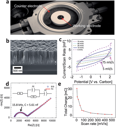 | ||
| Fig. 1 (a) Photograph of the in situ electrochemical AFM cell, (b) SEM micrograph of an edge of the CDC film, (c) cyclic voltammograms at various scan rates using a carbon cloth counter electrode, (d) electrochemical impedance spectrum of the cell (inset shows the RC model to which the data was fit) over a frequency range of 10 mHz to 100 kHz and using a single sine amplitude of 10 mV at open circuit potential (OCP). The fit parameters are provided in Table 1. (e) Total charge extracted by integration of the current over time as a function of scan rate. | ||
Electrochemical characterization was performed using a Bio-Logic SP-200 (Bio-Logic, USA) potentiostat/galvanostat in the 2-electrode setup (no reference electrode). Cyclic voltammograms were potentiostatically controlled. For Electrochemical Impedance Spectroscopy (EIS), we used an internal frequency response analyzer with a single sine amplitude of 10 mV over a range of 10 mHz to 100 kHz. Fitting of the Nyquist plot data was carried out using the EC Lab software (Bio-Logic, USA).
Surface displacement measurements were carried out by keeping the AFM tip in contact with the CDC sample with a constant contact force at a fixed location during charge and discharge recorded at the same rate as the current. In all experiments Pt coated Nanosensors™ (PPP-EFM-50, k = 0.5–9.5 N m−1) AFM tips were employed.
3 Results and discussion
The typical morphology of the CDC thin film electrode is shown in the scanning electron micrograph (SEM) in Fig. 1b. Conformal to the TiC thin film precursor, we note that the lateral grain morphology is semi-spherical with an average grain size on the order of 200–300 nm with a root mean square (RMS) roughness of ∼20 nm which is in good agreement with the AFM imaging (Fig. 2a). In addition to the lateral texture, from the SEM cross-section image (Fig. 1a) we can also see an axial texture of the columnar CDC grains which extends along the entire length of the thin film (i.e. ∼1 μm).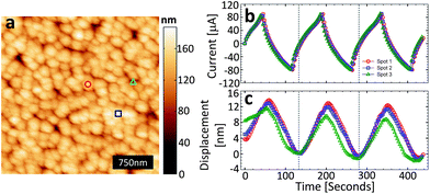 | ||
| Fig. 2 (a) AFM topography (3 μm × 3 μm) of the CDC surface in RTIL, the marks indicate the surface locations that correspond to the charge/discharge/strain cycles in (b and c), (b) potentiostatically controlled cyclic voltammogram (plotted as current versus time) at 50 mV s−1; three consecutive cycles for each of the three surface locations indicated with symbols in (a), and (c) strain response measured during the cyclic voltammetry tests (legend symbols are the same as in (a)). | ||
Basic electrochemical characterization is shown in Fig. 1c and d. Here, the differential capacitance (Fig. 1c) and the total charge as determined by integrating the current over time (Fig. 1e) is shown to increase with decreasing scan rate as observed previously.28 As seen from the CVs, the shape is indicative of a capacitive energy storage mechanism; yet we notice the pronounced resistive behavior of the electrode which is related to the setup and the lateral contact of the film electrode, which is located on an electrically insulated substrate. EIS reveals a Randles-like circuit (a constant phase element (CPE) replaces the capacitor in an RC circuit) in series with an additional CPE, which is commonly used to describe electrochemical double-layers.32 The values for the fitted elements of the equivalent circuit are provided in Table 1. The equivalent capacitance of Q2 (5.61 nF) shown in Fig. 1d was determined using the approach outlined by Hsu and Mansfeld.33 Here, the frequency at which −Im(Z) is maximum can be calculated using:
| fmax = 1/(2π[RQ]1/α) | (1) |
| C = Qfmaxα−1 | (2) |
Equivalent capacitance for Q3 could not be estimated as the Hsu model33 requires a parallel resistance.
The AFM topography of the CDC thin film measured in RTIL is shown in Fig. 2a. Note the topography is a convolution of the tip shape and the actual sample topography. The pores cannot be seen since their lateral size is much smaller than the tip radius of 20–30 nm. Fig. 2c shows the surface height change for three separate locations on the CDC surface during charge/discharge. Fig. 2b plots the charge/discharge current versus time (from the cyclic voltammograms) using a fixed scan rate of 50 mV s−1 and a voltage range from −1.5 V to 2.15 V for three cycles. It is important to note that the cyclic voltammograms are presented this way to offer a more intuitive comparison to the displacement curves. This voltage range was prior shown to be the stable window for this electrolyte, at least in a dry environment. However, the self-balancing nature of supercapacitors means that the maximum voltage difference between the electrodes using the two-electrode setup remained within 2.15 V, but the CDC electrode polarity was changed as the voltage sweep was conducted from −1.5 to 2.15 V. That is, both electrodes experienced positive and negative polarities without exceeding a potential difference ≥2.15 V. The repeatable electrochemical behavior shown in Fig. 2b suggests that degradation of the electrolyte did not have a significant effect on the results of these short-term tests.
We note the following:
(i) The displacement in the CDC film at 50 mV s−1 is on the order of 15 nm (∼1% assuming 1.5 μm thick CDC layer) over the course of the cycle, which is a factor of four smaller than the resolution limit of the typical ED transducer7 and would not be observable by ordinary ED measurements.
(ii) There is a phase lag between the charge/discharge current and the strain response.
(iii) Subtle variations in strain are observed as a function of spatial location, indicating that strain response exhibits spatial variability. Note that there is an additional monotone drift of the displacement data which is due to drift of the AFM Z-position control and which is not related to the sample.
To investigate the effect of scan rate on the strain response, we measured the height change of a fixed spot on the CDC electrode surface. Fig. 3a–c plots the current and strain response for 10, 100 and 500 mV s−1 respectively. Significant strain is observed for each of the scan rates, including the fastest one (500 mV s−1). However, the magnitude of the strain (peak to peak) decreases with increasing scan rate from ∼40 nm at 10 mV s−1 to ∼5 nm at 500 mV s−1. This behavior is similar to the reduced capacitance at higher scan rates (Fig. 1d) which is likely the result of incomplete charging of the capacitor (i.e., ions cannot access all the surface area of the micropores within the time of the charge/discharge cycle). Also, a clear phase lag exists between the current and strain responses at fast scan rates which decreases with the scan rate (127° at 500 and 7° at 10 mV s−1).
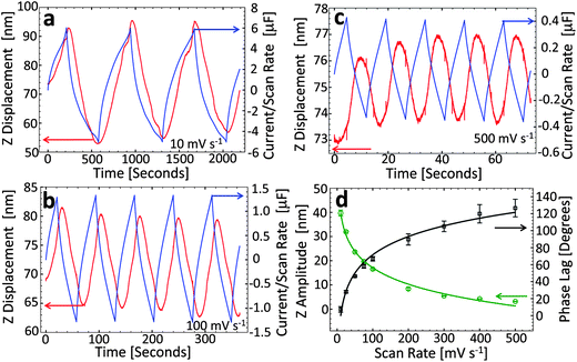 | ||
| Fig. 3 (a–c) Cyclic voltammograms and sample surface displacement curves collected with the tip in a fixed location on the CDC surface for scan rates of (a) 10 mV s−1, (b) 100 mV s−1, (c) 500 mV s−1 and (d) summary of maximum displacement (i.e., peak-to-peak amplitude of displacement signal) and phase lag (between current and displacement curves) as a function of scan rate. The curves in (d) are guides to the eye. | ||
The displacement–time curves at slow scan rates (∼10 mV s−1 and below) exhibit some fine structure. We found that this is the result of the lateral sample expansion which is more pronounced at slow charging rates and was found to be reproducible. Here, the sample roughness determines the error in the recorded sample height changes induced by this effect which is small compared to the recorded changes in Z. Fig. 3d presents a summary of the strain and phase lag as a function of scan rate. Interestingly, the strain response and phase lag experience an inversely proportional relationship where slow scan rates result in large strain and very little/no phase lag, while fast scan rates produce little strain, but the phase is shifted considerably (ca. 120 degrees at 500 mV s−1).
The phase lag between the current and the displacement (or, alternatively, the difference in phase lags between voltage and current and voltage and strain) suggests the presence of two different mechanisms which contribute to the capacitance and the sample volume changes. This is even more evident when the surface displacement is plotted versus the current divided by the scan rate as shown in Fig. 4a. The loops in the displacement–charge curves exhibit large area at slow scan rates and smaller areas with increasing scan rates. After each electric field reversal (vertex potential), the capacitance changes abruptly and strongly without significant strain changes. At one point, the strain starts to change together with a continued change in capacitance. This effect is more pronounced at slow scan rates.
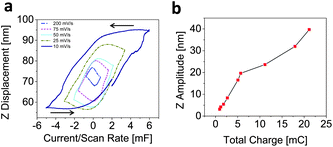 | ||
| Fig. 4 (a) Plot of displacement versus cell capacitance (current/scan rate) at various charge/discharge rates and (b) correlation between the total charge and the maximum surface displacement. | ||
To correlate the displacement with cell capacitance, Fig. 4b plots the maximum surface displacement (Z amplitude) against the total charge (Fig. 1e) at all the charge/discharge rates employed. We observe a monotonically increasing dependence between the maximum displacement and the charge. The data suggests that the strain response scales accordingly with the degree of charging of the capacitor, which implies that the processes responsible for inducing strain and storing charge are highly correlated. However, there seems to be a different correlation between them at large and small accumulated charge.
To explain the observed behavior, two charge-induced strain mechanisms should be discussed. First, pore swelling as described by Hantel et al.,7 through osmotic pressure and second, ion intercalation or insertion into the carbon material itself. For the latter, in theory, this can be accomplished either by RTIL ions (which is rather unlikely regarding the large size of the ions, ∼0.9 nm for Bmim and ∼0.8 nm for Tf2N) or the added Li-ions in the RTIL (which is frequently observed for graphitic anodes of lithium-ion battery). However, low-temperature CDC is amorphous and no graphite was found in the CDC structure.7,34 Due to the absence of a redox couple (if we ignore possible interaction between the electrolyte and adsorbed water and other impurities) and insertion capable material in the presented electrochemical system, the pore filling effect is expected to be dominant. We have recently shown35 that addition of smaller ions allows a more efficient pore occupancy due to filling small pores that cannot be occupied by larger ions (RTIL cations, in our case), so we expect Li+ to occupy the smallest pores in the CDC network.
The way charge storage was traditionally described in EDLC electrodes, with ions adsorbed on both pore walls, cannot happen in our material since there is no space available for more than one ion per a sub-nanometer pore of CDC.7 In the confined nano-pores, where there is not enough room to build the complete “double layer” structure, such as defined by Helmholtz, the ions penetrate into pores of matching size.1 This differs from graphite intercalation, since there is no electron density inside pores and the process is physical in nature. However, the ions may have to penetrate through narrow bottlenecks between pores, and ions of opposite charge are expected to move simultaneously when charge is applied36 leading to a kind of “traffic jam” and swelling of the carbon network, which is a dynamic effect. It is also important to mention that when the potential sign is changed, ions of the opposite sign start replacing the ones sitting in pores. However, an experiment using a 3-electrode configuration will be required to correlate the strain to the behavior of specific ions. Repulsion between the oppositely charged ions and other effects may also be responsible for the observed strain, but their exact identification will require a computational effort, in addition to in situ experiments.
Depending on the size and shape of the pores, the ion transport through the porous carbon network adds a characteristic time scale to the system, which is responsible for the observed phase lag between the current and strain. If the Z–V curves are not convoluted with the capacitance but simply plotted against the applied voltage as displayed in Fig. 5, this characteristic time can be extracted.
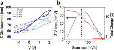 | ||
| Fig. 5 (a) Plot of Z displacement versus applied voltage at various charge/discharge rates (in all cases the initial direction of the potential sweep was anodic) and (b) correlation between area of the Z–V curves and total charge and the scan rate. Note: the Z-displacement curves for scan rates of 200–500 mV s−1 were omitted for visual clarity. | ||
Fig. 5a shows a continuous increase in maximum Z displacement with decreasing scan rate as was also demonstrated in Fig. 3d. Note the loops are hysteretic and the loop area increases with decreasing scan rate until a maximum is reached (Fig. 5b). At very low scan rates, the Z–V curves are non-hysteretic, indicating that the ion migration into the electrode pores is occurring under equilibrium-like conditions. This can be further elaborated upon by considering the following two dynamic regimes. (i) The fast scan regime being one which probes too quickly to allow for sufficient ion migration into the porous carbon network to respond to the applied potential during the voltage sweep. Therefore the Z-displacement lags behind as noted in Fig. 3d, which leads to the observed hysteresis (i.e. larger loop area). (ii) In the slow scan regime, the potential is swept at a rate comparable to or slower than the ion migration process, therefore leading to non-hysteretic response. This suggests that the system is approaching “equilibrium conditions,” that is, the time scales of charging and migration are approximately equal. This observation is further supported by the fact that the total charge (i.e. capacitance) deviates from the linear regime towards a rate-independent regime as shown in the log–log plot in Fig. 5b. The maximum in the Z–V area versus scan rate curve at ∼50 mV s−1 shows clearly a cross-over between the two regimes described above. However, the transition is not sharp, but rather distributed around this scan rate.
The characteristic time for ion migration into the pores can be determined from the maximum of the Z–V loop area in Fig. 5b. This is achieved by dividing the voltage range to complete a full charge/discharge cycle (twice the voltage window of 3.65 V) by 50 mV s−1 (maximum in Fig. 5b), which results in a characteristic time of 146 s. This characteristic time represents the time required to achieve double layer/pore saturation. Additionally, this maximum corresponds to a scan frequency of ∼6.8 mHz, which would be observed at the low frequency end (linear region) of the EIS plot shown in Fig. 1d. Recall that the linear region is described by CPE Q3 in the equivalent circuit. This suggests that the half-circle defined by the parallel R2–Q2 circuit describes the fast double layer contribution, as opposed to the much slower strain generating ion-insertion/migration contribution.
Nanoscale dilatometry thus allows for the extraction of the different time scales on which these processes happen. From the EIS, we can estimate the RC time constant (using τ = RC) for the semicircle in Fig. 1c describing the electric double layer (i.e. the fast charging of the double layer) using eqn (2) to be approximately 15.9 μs. As noted above, the equivalent capacitance of Q3 cannot be extracted by the same procedure. However, the nanoscale dilatometry procedure outlined here provides a characteristic time for ion migration into carbon network and pores of ∼146 s. A simple comparison suggests that the time scale of the fast double layer contribution, is ∼9 × 10⁶ times faster than that of the mass transport migration process which leads to the observed strain. This explains why exohedral carbons, such as nanotubes and nano onions, can be charged up to 1000 times faster than porous carbon electrodes.1
These experimental findings fit well with recent work that analyzed the ion transport dynamics in porous EDLC electrodes.36–39 We expect that the comparison of experimental data based on nanoscale electrochemical dilatometry with predictive modeling will allow the determination of the characteristic length scale of Debye lengths and extract migration times of ions within the electric double layer and into the pores of the sample.
4 Conclusions
We have presented a method to perform nanoscale electrochemical dilatometry using atomic force microscopy and have adapted it to study CDC film electrodes. With this method it is possible to study different processes contributing to capacitance based on strain generation and to assign these physical processes to the elements of the equivalent circle of the EIS. Fast and slow processes could be identified, both of which contribute to the capacitance but only one to strain. The fast process is assigned to the double layer charging whereas the slow process is assigned to ion migration into the carbon pores or through the porous carbon matrix. The high spatial resolution provided by this method will facilitate the investigation of spatial variability and develop structure–function relationships which can be used for future material design.Acknowledgements
Support was provided by the Fluid Interface Reactions, Structures and Transport (FIRST), a National Laboratory Energy Frontier Research Center funded by the U.S. Department of Energy, Office of Science, Office of Basic Energy Sciences and the Center for Nanophase Materials Sciences, which is sponsored at Oak Ridge National Laboratory by the Scientific User Facilities Division, Office of Basic Energy Sciences, U.S. Department of Energy. VP acknowledges funding from the German Federal Ministry for Research and Education (BMBF) in support of the nanoEES3D project (award number 03EK3013) as part of the strategic funding initiative energy storage framework. We are thankful to J. Hettinger (Rowan University) for help with TiC film sputtering. The authors would also like to thank Jennifer M. Black for insightful discussions.References
- P. Simon and Y. Gogotsi, Acc. Chem. Res., 2012 DOI:10.1021/ar200306b.
- P. Simon and A. Burke, Electrochem. Soc. Interface, 2010, 17, 38–43 Search PubMed.
- J. R. Miller and P. Simon, Electrochem. Soc. Interface, 2008, 17, 31–32 CAS.
- M. Galinski, A. Lewandowski and I. Stepniak, Electrochim. Acta, 2006, 51, 5567–5580 CrossRef CAS.
- V. Subramanian, H. W. Zhu, R. Vajtai, P. M. Ajayan and B. Q. Wei, J. Phys. Chem. B, 2005, 109, 20207–20214 CrossRef CAS.
- M. Hahn, O. Barbieri, F. P. Campana, R. Kötz and R. Gallay, Appl. Phys. A: Mater. Sci. Process., 2006, 82, 633–638 CrossRef CAS.
- M. M. Hantel, V. Presser, R. Kötz and Y. Gogotsi, Electrochem. Commun., 2011, 13, 1221–1224 CrossRef CAS.
- P. W. Ruch, R. Kötz and A. Wokaun, Electrochim. Acta, 2009, 54, 4451–4458 CrossRef CAS.
- M. Hahn, O. Barbieri, R. Gallay and R. Kötz, Carbon, 2006, 44, 2523–2533 CrossRef CAS.
- M. M. Hantel, T. Kaspar, R. Nesper, A. Wokaun and R. Kötz, Electrochem. Commun., 2011, 13, 90–92 CrossRef CAS.
- L.-H. Shao, J. Biener, H.-J. Jin, M. M. Biener, T. F. Baumann and J. Weissmüller, Adv. Funct. Mater., 2012, 22, 3029–3034 CrossRef CAS.
- J. Torop, M. Arulepp, J. Leis, A. Punning, U. Johanson, V. Palmre and A. Aabloo, Materials, 2010, 3, 9–25 CrossRef CAS.
- J. O. Besenhard, M. Winter, J. Yang and W. Biberacher, J. Power Sources, 1995, 54, 228–231 CrossRef CAS.
- W. Biberacher, A. Lerf, J. O. Besenhard, H. Mohwald and T. Butz, Mater. Res. Bull., 1982, 17, 1385–1392 CrossRef CAS.
- T. Ohzuku, N. Matoba and K. Sawai, J. Power Sources, 2001, 97-8, 73–77 CrossRef.
- M. Winter, G. H. Wrodnigg, J. O. Besenhard, W. Biberacher and P. Novak, J. Electrochem. Soc., 2000, 147, 2427–2431 CrossRef CAS.
- D. Pech, M. Brunet, H. Durou, P. H. Huang, V. Mochalin, Y. Gogotsi, P. L. Taberna and P. Simon, Nat. Nanotechnol., 2010, 5, 651–654 CrossRef CAS.
- N. Balke, S. Jesse, A. N. Morozovska, E. Eliseev, D. W. Chung, Y. Kim, L. Adamczyk, R. E. Garcia, N. Dudney and S. V. Kalinin, Nat. Nanotechnol., 2010, 5, 749–754 CrossRef CAS.
- T. M. Arruda, A. Kumar, S. V. Kalinin and S. Jesse, Nano Lett., 2011, 11, 4161–4167 CrossRef CAS.
- T. M. Arruda, A. Kumar, S. V. Kalinin and S. Jesse, Nanotechnology, 2012, 23, 325402 CrossRef.
- H. J. Butt, B. Cappella and M. Kappl, Surf. Sci. Rep., 2005, 59, 1–152 CrossRef CAS.
- M. Jaafar, D. Martinez-Martin, M. Cuenca, J. Melcher, A. Raman and J. Gomez-Herrero, Beilstein J. Nanotechnol., 2012, 3, 336–344 CrossRef CAS.
- O. Marti, B. Drake and P. K. Hansma, Appl. Phys. Lett., 1987, 51, 484–486 CrossRef CAS.
- K. O. Vanderwerf, C. A. J. Putman, B. G. Degrooth and J. Greve, Appl. Phys. Lett., 1994, 65, 1195–1197 CrossRef CAS.
- R. Atkin, N. Borisenko, M. Drueschler, S. Z. El Abedin, F. Endres, R. Hayes, B. Huber and B. Roling, Phys. Chem. Chem. Phys., 2011, 13, 6849–6857 RSC.
- F. Endres, N. Borisenko, S. Zein El Abedin, R. Hayes and R. Atkin, Faraday Discuss., 2012, 154, 221–233 RSC.
- R. Hayes, N. Borisenko, M. K. Tam, P. C. Howlett, F. Endres and R. Atkin, J. Phys. Chem. C, 2011, 115, 6855–6863 CAS.
- M. Heon, S. Lofland, J. Applegate, R. Nolte, E. Cortes, J. D. Hettinger, P.-L. Taberna, P. Simon, P. Huang, M. Brunet and Y. Gogotsi, Energy Environ. Sci., 2011, 4, 135–138 CAS.
- S. H. Yeon, I. Knoke, Y. Gogotsi and J. E. Fischer, Microporous Mesoporous Mater., 2010, 131, 423–428 CrossRef CAS.
- R. Dash, J. Chmiola, G. Yushin, Y. Gogotsi, G. Laudisio, J. Singer, J. Fischer and S. Kucheyev, Carbon, 2006, 44, 2489–2497 CrossRef CAS.
- A. K. Burrell, R. E. D. Sesto, S. N. Baker, T. M. McCleskey and G. A. Baker, Green Chem., 2007, 9, 449–454 RSC.
- L. Permann, M. Latt, J. Leis and M. Arulepp, Electrochim. Acta, 2006, 51, 1274–1281 CrossRef CAS.
- C. H. Hsu and F. Mansfeld, Corrosion, 2001, 57, 747–748 CrossRef CAS.
- G. Laudisio, R. K. Dash, J. P. Singer, G. Yushin, Y. Gogotsi and J. E. Fischer, Langmuir, 2006, 22, 8945–8950 CrossRef CAS.
- J. Segalini, E. Iwama, P. L. Taberna, Y. Gogotsi and P. Simon, Electrochem. Commun., 2012, 15, 63–65 CrossRef CAS.
- C. Merlet, B. Rotenberg, P. A. Madden, P. L. Taberna, P. Simon, Y. Gogotsi and M. Salanne, Nat. Mater., 2012, 11, 306–310 CrossRef CAS.
- M. Z. Bazant, B. D. Storey and A. A. Kornyshev, Phys. Rev. Lett., 2011, 106, 046102 CrossRef.
- P. M. Biesheuvel and M. Z. Bazant, Phys. Rev. E: Stat., Nonlinear, Soft Matter Phys., 2010, 81, 031502 CrossRef CAS.
- P. M. Biesheuvel, Y. Q. Fu and M. Z. Bazant, Phys. Rev. E: Stat., Nonlinear, Soft Matter Phys., 2011, 83, 061507 CrossRef CAS.
| This journal is © The Royal Society of Chemistry 2013 |