 Open Access Article
 This Open Access Article is licensed under a
 Creative Commons Attribution 3.0 Unported Licence
Effects of atomic scale roughness at metal/insulator interfaces on metal work function
Sanliang Linga, Matthew B. Watkinsa and Alexander L. Shlugerab
aDepartment of Physics and Astronomy, University College London, Gower Street, London WC1E 6BT, UK. E-mail: S.Ling@ucl.ac.uk
bLondon Centre for Nanotechnology, University College London, 17-19 Gordon Street, London WC1H 0AH, UK
First published on 26th September 2013
Abstract
We evaluate the performance of different van der Waals (vdW) corrected density functional theory (DFT) methods in predicting the structure of perfect interfaces between the LiF(001), MgO(001), NiO(001) films on the Ag(001) surface and the resulting work function shift of Ag(001). The results demonstrate that including the van der Waals interaction is important for obtaining accurate interface structures and the metal work function shift. The work function shift results from a subtle interplay of several effects strongly affected by even small changes in the interface geometry. This makes the accuracy of theoretical methods insufficient for predicting the shift values better than within 0.2 eV. Most of the existing van der Waals corrected functionals are not particularly suited for studying metal/insulator interfaces. The lack of accurate experimental data on the interface geometries and surface rumpling of insulators hampers the calibration of existing and novel density functionals.
1 Introduction
Insulator thin films supported on metal substrates are widely used in heterogeneous catalysis,1–3 microelectronics,4,5 molecular electronics,6 as cold electron emitters7 and photocathodes.8,9 Studying such films provides a solution to charging problems, which hamper the study of wide band gap insulators by scanning tunnelling microscopy, electron spectroscopies and other surface science techniques based on electrically charged probes. The interaction between a metal substrate and an insulator thin-film determines the electronic properties of these interfaces and affects the characteristics of both components. For example, insulator thin films may shift the work function of the underlying metal substrate10 and electron transfer from the metal may affect the charge states of defects in the insulator.11 However, accurately measuring the interface geometry, the ensuing adhesion energy, and the electronic structure changes of both the metal and the insulator is notoriously difficult due to the well-known uncertainties in the film preparation and probing procedures.11,12 Therefore our understanding of these systems owes much to the development of material modelling methods.13 In this paper we demonstrate that the accuracy of these methods is still insufficient for making quantitatively reliable predictions and well-defined test systems are needed for their calibration. We focus on predicting the interface distance and the metal work function shift, Δϕ, as these are strong effects that can be measured by several experimental methods.14,15 The results of some of these measurements are summarized in Table 1.The metal/insulator interface distance is one of the most important factors that affect the local Δϕ. It is determined by the balance between the short-range (e.g. ionic or covalent bonding) and long-range (e.g. image and van der Waals) interactions.16 As pointed out by Jupille et al., in the limit of a noble metal interacting with a wide band gap insulator, the adhesion energy is dominated by long-range interactions.16 The theoretical description of such interfaces based on conventional DFT functionals may therefore fail to predict the correct interface geometry and adhesion energy as they do not capture long-range instantaneous electron correlation effects responsible for the van der Waals interactions.17,18 For example, Levchenko et al.19 recently used a hierarchy of DFT methods including PBE, HSE06, and the state-of-the-art exact exchange plus correlation in the random phase approximation (EX-cRPA/cRPA+) to calculate the adhesion energies of AuN clusters (N > 1) supported on MgO(100) surfaces and found that the van der Waals interaction, missing in PBE and HSE06 methods but accounted for by the EX-cRPA/cRPA+ method, makes a significant contribution to the adhesion energy of AuN clusters. It is therefore reasonable to assume that the van der Waals interaction may also play an important role in describing the properties of insulator thin films supported on metal substrates.
However, using accurate methods, such as EX-cRPA/cRPA+, to account for the van der Waals interaction at metal/insulator interfaces is extremely expensive and calculating forces with such methods is still a challenge. It is desirable to have a method that is relatively cheap and yet can correctly describe the van der Waals and other interactions at metal/insulator interfaces in a self-consistent manner. The recently developed van der Waals corrected DFT methods20–22 in principle provide such a possibility, but their accuracy has not yet been tested on real metal/insulator systems. They must describe the subtle interplay of three main effects that determine metal Δϕ due to adsorption of an insulator thin film:23,24 (i) Coulomb repulsion of metal electron density by insulator anions, which reduces the intrinsic metal surface dipole originating from electron density spilling out of the metal surface, and this decreases the effective work function of the interface system; (ii) interfacial charge transfer across the interface, which creates an interfacial dipole, either pointing towards the metal (electron transfer from insulator to metal) and decreasing the effective work function of the interface system, or pointing towards the insulator (electron transfer from metal to insulator) and increasing the effective work function of the interface system; (iii) insulator rumpling, which creates a dipole due to the finite separation between anionic and cationic atomic layers in an insulator, and this can either decrease the effective work function, if the anion is sitting closer to the metal substrate, or increase the effective work function, if the cation is sitting closer to the metal substrate. These effects are schematically presented in Fig. 1. We note that the effects of dipoles due to interfacial charge transfer and insulator rumpling on metal work function can be discussed in terms of the parallel plate capacitor model,25 which has been applied successfully in theoretical studies of self-assembled organic monolayers on metal substrates.26,27
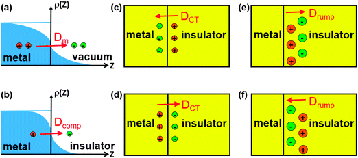 | ||
| Fig. 1 Various mechanisms that affect the shift of metal work function in contact with an insulator thin film. (a) Electron density spilling out of the metal surface naturally into the vacuum, creating a surface dipole Dm pointing outwards from the metal surface; (b) upon insulator deposition, due to Coulomb repulsion of the metal electron density by insulator anions, the metal surface dipole is decreased, resulting in a smaller surface dipole (denoted as Dcomp), and this decreases the effective work function; (c) electrons transfer from insulator to metal, resulting in a “positive” insulator and a “negative” metal, which creates an interfacial dipole (denoted as DCT) pointing towards the metal substrate and decreases the effective work function; (d) electrons transfer from metal to insulator, resulting in a “negative” insulator and a “positive” metal, which creates an interfacial dipole (denoted as DCT) pointing towards the insulator and increases the effective work function; (e) a rumpled insulator layer at the interface, i.e. cations sitting closer to the metal substrate, which creates an intrinsic dipole inside the insulator (denoted as Drump) pointing towards the insulator and increases the effective work function; (f) a rumpled insulator layer at the interface, i.e. anions sitting closer to the metal substrate, which creates an intrinsic dipole inside the insulator (denoted as Drump) pointing towards the metal substrate and decreases the effective work function. | ||
In this paper, we evaluate different van der Waals corrected DFT methods implemented in the VASP code using three model systems: LiF, MgO and NiO layers on the Ag(001) substrate. We optimize the interface geometries to compare the resulting interface structures and then discuss the effects on the shift of metal work function due to variations in the interface distance and insulator rumpling, as predicted by different methods. Thin MgO films on the Ag(001) surface have been studied extensively both experimentally14,15,28–38 and theoretically10,23,39–43 and are known to be rough on the nanoscale, forming some islands.30,37,38 Therefore Δϕ depends strongly on the film quality and morphology (see Table 1). However, not much is known about Δϕ at LiF/Ag and NiO/Ag interfaces. The effect of the film roughness has been discussed in our previous work.43 Here we demonstrate how different geometric factors at the interface of a perfectly matched flat insulator thin film affect the work function of the metallic support.
2 Methods of calculations
The three interface systems, LiF/Ag(001), MgO/Ag(001) and NiO/Ag(001), were selected based on the following considerations: (i) the lattice mismatch between Ag(001) and the three insulators is relatively small, −1.9%, 2.4% and 1.0%, respectively, minimizing the effects of interface strain; (ii) the band gaps of LiF, MgO and NiO range from 13.6, to 7.8 and 4.3 eV. It is expected that the NiO/Ag(001) interface, due to the small band gap of NiO compared with the other two insulators, would have more interfacial charge transfer, and stronger covalent character in the interface binding. On the other hand, the interaction between LiF and Ag may be expected to be weaker, with much less interfacial charge transfer, and thus the interface binding is more likely to be dominated by the van der Waals interaction. MgO, which has an intermediate band gap, is expected to exhibit both effects.43 Studying geometrically similar but electronically different interface systems enables us to understand better the effect of van der Waals interactions on the interface geometry and Δϕ.In addition to the conventional PBE method, the following van der Waals corrected DFT methods are considered: PBE + D2,44 PBE + TS,45 PBE + TS + SCS,46 optPBE,47 and vdW-DF2.48 For lattice parameters of isolated bulk materials, we also considered a meta-GGA, M06L.49 Depending on how the van der Waals interactions are included, these methods can be divided into three groups, i.e. a posteriori methods, including PBE + D2, PBE + TS, which add on top of the conventional PBE energy an additional van der Waals interaction term (represented by an additive pairwise C6/r6 expression), the non-local correlation functionals, including optPBE and vdW-DF2, which add non-local corrections to local or semi-local correlation functionals, and calculate the electronic structure in a self-consistent way, and PBE + TS + SCS where many-body screening effects are included to some degree.
For the first group of methods, different approaches exist to obtain C6 dispersion coefficients. For example, PBE + D2 calculates C6 coefficients as a function of the ionization potential and static polarizability of isolated atoms. While this approach exhibits good performance on the S22 database,50 there are two problems that might affect its performance for the metal/insulator interface systems: the lack of dependence of the C6 coefficients on different chemical environments and using the isolated atom as a reference can be inadequate when this atom forms a strong ionic bond with another atom. These problems are somewhat alleviated if one uses the PBE + TS and PBE + TS + SCS methods developed by Tkatchenko and co-workers. In the PBE + TS method,45 the atomic C6 coefficients are dependent upon their chemical environments by employing a Hirshfeld partitioning of the electron density to determine the effective volume for an atom inside a molecule/solid. This partition is then used as a scaling factor to calculate the effective atomic polarizability and the effective atomic C6 coefficients. The PBE + TS + SCS method goes a step further by solving the self-consistent screening equation of the frequency-dependent polarizability, which is then used to calculate the effective C6 coefficients. Such an approach enables one to take into account the effect of the dynamic electric field produced by the surrounding polarizable atoms on the effective C6 coefficient of a particular atom.
For the second group of methods, the conventional DFT functionals are supplemented with an extra non-local correlation energy term, which is represented by a double space integral of the electron density, with the integral kernel expressed by a pairwise formula.22 Different non-local correlation functionals have been proposed, and also different exchange functionals were employed. Many of these functionals have been reported to show qualitatively different results for molecular complexes47 and adsorption of organic molecules on surfaces of inorganic solids,51,52 compared with conventional GGA functionals. In this study we assess the performance of two typical non-local correlation functionals, optPBE and vdW-DF2.
While the first and third groups of methods do not modify the electronic structure of the interface other than indirectly through changing the interface geometry, the second group of methods solve the Kohn–Sham equation self-consistently and thus modify both the electronic structure as well as the geometry of an interface. Note that the performance of the second group of methods on the electronic structure of solid-state materials has not been fully tested and validated against high-level theoretical or experimental results, and it is not clear whether they provide correct band offsets at metal/insulator interfaces. Since performing such a benchmarking is beyond the scope of this paper, we use these methods only to obtain interface geometries.
Describing electron transfer between a metal and an insulator requires accurately calculating the band offset at the interface. Conventional GGA functionals, e.g. PBE and PW91, systematically underestimate band gaps of insulators.53 Therefore, we have performed electronic structure calculations for all the three metal/insulator interfaces with a screened hybrid functional (HSE06),54 which predicts reasonable insulator band gaps and is expected to better describe band offsets at the interfaces as well as the interfacial charge transfer. However, due to the computational demands of such hybrid functional calculations on mixed metal/insulator systems, the HSE06 calculations are single point electronic structure calculations at interface geometries optimized at PBE or PBE + D2 level.
We assume that a thin film of insulator is grown on top of the metal substrate and follows pseudomorphic growth. In other words, due to the relatively small (less than 5%) lattice mismatch between the two materials, the insulator is forced to adopt the lattice parameter of the metal substrate. Therefore, for all the three interfaces, we used Ag lattice parameters (as determined using the PBE functional) for constructing unit cells of interface slabs along X and Y directions. The most stable interface configuration was considered, with the anion located directly above the Ag atom and the cation above hollow sites. The smallest asymmetric unit cell included four layers of Ag and three layers of insulator (with a non-polar (001) surface). For NiO, we considered an antiferromagnetic (AFM2) magnetic structure of the Ni atoms. Therefore, each Ag layer has one (for LiF/Ag and MgO/Ag) or two (for NiO/Ag) Ag atoms, and each insulator layer has two (for LiF and MgO) or four (for NiO) atoms.
All calculations are performed using the Vienna Ab initio Simulation Package (VASP 5.3.3).55 A plane wave basis set with a 400 eV energy cutoff was employed to represent the wavefunctions, and the projector augmented wave (PAW) method56 was employed. For LiF and MgO a spin-unpolarized DFT method and for NiO a spin-polarized DFT + U method (with or without van der Waals corrections) were used. Following the previous calculations,24 a U value of 4.0 eV was used for d-electrons of Ni atoms in the interface layer of NiO to take into account the metal screening in the insulator, and a U value of 5.3 eV was used for d-electrons of Ni atoms in the surface and middle layers. Geometry optimizations of interface slabs were considered converged if the maximum force on relaxed atoms falls below 0.01 eV Å−1. Monkhorst–Pack k-point grids57 of (9 × 9 × 9) and (12 × 12 × 1) were used for isolated bulk materials and heterogeneous interface slabs, respectively. A vacuum layer exceeding 40 Å was used throughout the current study to reduce the artificial interaction between periodic images of interface slabs and to converge the electrostatic potential in the vacuum. Dipole corrections have been applied throughout the current study to eliminate interactions between total dipole moments of repeated interface slabs along the Z direction. All charge analyses were performed using a Bader method58 based on the tools developed by Henkelman and co-workers.59
3 Results of calculations
3.1 Lattice parameters
The heterogeneous interfaces considered in this study include structurally similar (with small lattice mismatch) but electronically different (with different band gaps) insulators. Therefore it is important that a computational method gives equally good descriptions for the lattice parameters of both the metal and the insulator at the interface. The theoretical lattice parameters of the four materials considered in the current study, Ag, LiF, MgO and NiO, calculated with different methods are shown in Table 2. We also listed relevant experimental lattice parameters in Table 2 for reference, in which the experimental lattice parameters of Ag, LiF and MgO were taken from ref. 60, and the experimental lattice parameter of NiO was taken from ref. 61.| PBE | PBE + D2 | PBE + TS | PBE + TS + SCS | optPBE | vdW-DF2 | M06L | Expt. | |
|---|---|---|---|---|---|---|---|---|
| Ag | 4.15 | 4.15 | 4.07 | 4.12 | 4.18 | 4.26 | 4.19 | 4.069 |
| LiF | 4.07 | 4.07 | 3.67 | 3.98 | 4.07 | 4.07 | 3.99 | 4.010 |
| MgO | 4.25 | 4.19 | 4.19 | 4.22 | 4.25 | 4.27 | 4.19 | 4.207 |
| NiO | 4.19 | 4.19 | 4.16 | 4.19 | 4.19 | 4.31 | 4.23 | 4.195 |
One can see that all methods (except PBE + TS + SCS) overestimate the lattice constant of Ag. Notably vdW-DF2 overestimates by 4.7%, compared with 2.0% of PBE. This behaviour has also been observed in several previous studies.62,63 A similar overestimation of the Ag lattice parameter was also observed for optPBE, which can be regarded as belonging to the same family as the vdW-DF2 method, as both methods employ a non-local correlation functional to account for the van der Waals interaction and both methods were validated against the S22 data set consisting of molecular complexes. It is therefore important that metallic systems are included in fitting balanced vdW functionals for these types of metal/insulator interface systems.
We note that both schemes developed by Tkatchenko et al. (PBE + TS and PBE + TS + SCS) predict smaller lattice parameters for the four materials compared with PBE. This effect is most significant in the case of LiF, where the PBE + TS method gives a lattice parameter of 3.67 Å, almost 10% smaller than PBE. Similar underestimation of the lattice parameters by PBE + TS has also been reported for NaCl and KI,64 indicating that the PBE + TS method strongly overestimates the strength of van der Waals interactions in alkali halides. This is due to the fact that the Hirshfeld partitioning employed by the PBE + TS method fails for ionic solids with strong charge transfer character,65 such as alkali halides. These strongly ionic systems are too far from the atomic reference for which the C6 coefficients are calculated for the scaling based on atomic volumes to provide a good approximation. This problem is partially solved in the PBE + TS + SCS method, in which the underestimation of lattice parameters was reduced due to damping of the ionic polarizabilities by solving the self-consistent screening equation of the frequency-dependent polarizability,46e.g. the lattice parameter of LiF with PBE + TS + SCS is underestimated only by 2.2% compared with PBE.
3.2 Atomic scale roughness at the metal/insulator interfaces
The interface distance affects all three main factors that contribute to the shift of metal work function, including the Pauli repulsion of metal electrons by anions of the insulator thin film, electron transfer across the interface, and the insulator rumpling. Note that the interfacial charge transfer and the insulator rumpling are interrelated, and it is difficult to separate them from each other, i.e. the insulator rumpling can be regarded as a structural response to the interfacial charge transfer,66 and on the other hand, the interfacial charge transfer might be counterbalanced by the insulator rumpling. Therefore it is important to obtain accurate interface structure through minimizing the forces on all atoms at a given level of theory. We note that, because the interface distance and insulator rumpling are interrelated, attempts to fix insulator rumpling while scanning the potential energy as a function of the interface distance may lead to incorrect interface geometries.In the current study, the interface distance is defined between the Ag atoms and anions at the interface (denoted as dint, see Fig. 2b). The definition of the insulator rumpling is more complicated, as we are dealing with a three-layer insulator thin film, and rumpling may exist in all three layers. As the first step, we define the insulator rumpling of the interface layer (denoted as drump_int, see Fig. 2b) as the difference in the Z coordinates of cations and anions at the metal/insulator interface: if cations are closer to the metal substrate, this is defined as positive rumpling, and if anions are closer to the metal substrate, negative rumpling. Note that rumpling also exists in the top two layers of the insulator (denoted as drump_mid and drump_surf, respectively, see Fig. 2b), due to propagation of insulator rumpling at the interface layer and intrinsic rumpling due to different polarizabilities of anions and cations at the surface layer.67
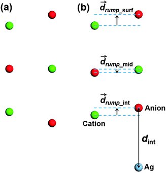 | ||
| Fig. 2 Schematic illustrating the definitions of the interface distance and insulator rumpling in (a) free-standing and (b) metal-supported insulator thin film used in this paper. | ||
Rumpling in each insulator layer produces different dipole moments along the direction which is given by the relative positions of cations and anions, and the magnitude is determined by the charges on ions as well as the separation of the cationic and anionic atomic layers (difference in Z coordinates). As the first approximation, we consider three dipole moments due to rumpling in each insulator layer and neglect the dipole–dipole interactions, as well as different separations between each insulator layer given by different methods. Then the final dipole moment intrinsic to the whole system is a vector sum of the three dipole moments given by each insulator layer. If we neglect the difference in the charges on anions and cations in each insulator layer, the dipole moment in each insulator layer can be directly correlated to the insulator rumpling in each layer. In this way, the total dipole moment intrinsic to the insulator slab can be described by only one parameter, i.e. the total insulator rumpling (denoted as drump_tot, see Table 3), which is a vector sum of the insulator rumpling present in each insulator layer. Below we discuss these geometric components of the interface in more detail.
| PBE | PBE + D2 | PBE + TS | |||||||
|---|---|---|---|---|---|---|---|---|---|
| dint | drump_int | drump_tot | dint | drump_int | drump_tot | dint | drump_int | drump_tot | |
| LiF | 2.98 | −0.035 | 0.025 | 2.56 | 0.045 | 0.093 | 2.59 | −0.015 | 0.073 |
| MgO | 2.70 | 0.012 | 0.045 | 2.51 | 0.034 | 0.073 | 2.52 | 0.027 | 0.073 |
| NiO | 2.53 | 0.053 | 0.073 | 2.52 | 0.059 | 0.069 | 2.41 | 0.071 | 0.098 |
| PBE + TS + SCS | optPBE | vdW-DF2 | |||||||
|---|---|---|---|---|---|---|---|---|---|
| dint | drump_int | drump_tot | dint | drump_int | drump_tot | dint | drump_int | drump_tot | |
| LiF | — | — | — | 2.94 | −0.026 | 0.029 | 2.92 | −0.039 | 0.003 |
| MgO | 2.37 | 0.061 | 0.108 | 2.69 | 0.016 | 0.044 | 3.04 | −0.006 | 0.022 |
| NiO | 2.31 | 0.097 | 0.133 | 2.50 | 0.059 | 0.069 | 2.73 | 0.031 | 0.034 |
One can see that the general trend of the interface distance follows LiF/Ag > MgO/Ag > NiO/Ag, which reflects different strengths of the interaction between Ag and the three different insulators. As a simple rule of thumb, this ordering follows the ordering of insulator band gaps: LiF (14.2 eV) > MgO (7.8 eV) > NiO (4.3 eV). More strictly speaking, the adhesion between Ag and an insulator is determined by the relative position of the Ag Fermi level with respect to the top of the valence band and the bottom of the conduction band of the insulator.
As shown in Table 3, as a result of the van der Waals corrections, the interface distances for all three model systems are further reduced, and for LiF/Ag, this reduction can be as big as 0.4 Å using the PBE + D2 and PBE + TS methods. We note that this value might be overestimated due to the fact that the dispersion coefficients were predetermined and kept fixed during the calculations within the PBE + D2 method. PBE + TS also tends to overestimate the strength of van der Waals interactions in alkali halides. On the other hand, optPBE gives a similar interface distance to PBE. The vdW-DF2 method predicts even larger interface distances of 3.04 Å for MgO/Ag and 2.73 Å for NiO/Ag, which are by 0.3 Å and 0.2 Å larger than those of PBE, respectively, and appear to be too large compared to available experimental data (see Table 1). This indicates that the performance of these functionals needs to be further tested and validated against data sets which include high-level experimental or theoretical data on metal/insulator interfaces.
Comparing the reductions in interface distances due to the inclusion of various van der Waals corrections, LiF/Ag (0.4 Å) shows the biggest reduction, followed by MgO/Ag (0.2 Å with PBE + D2 and PBE + TS methods) and NiO/Ag (0.1 Å with PBE + TS). This reflects the interplay of the van der Waals and covalent forces in the three interface systems. For the weakly interacting LiF/Ag interface with essentially no interfacial charge transfer, the van der Waals interaction dominates the binding and thus larger reduction in the interface distance is expected if the van der Waals correction is included. For MgO/Ag and NiO/Ag, where there is some interfacial charge transfer, covalent forces start to compete with the van der Waals interaction, or even dominate. Therefore the reduction in interface distance is smaller (for MgO/Ag) and can even be neglected (for NiO/Ag).
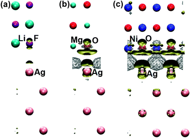 | ||
| Fig. 3 Electron density differences between (a) LiF/Ag, (b) MgO/Ag, and (c) NiO/Ag interface systems (with PBE geometries) and summations of electron densities of isolated Ag and insulator (LiF/MgO/NiO) slabs. Wireframes and solid hypersurfaces indicate electron density accumulation and reduction in the interface system, respectively. | ||
The change of sign of the insulator rumpling at the interface layer of LiF/Ag from PBE geometry to PBE + D2 geometry is probably an artefact owing to the fact that the PBE + D2 method used the atomic polarizability of a lithium atom (which is very polarizable) to calculate the dispersion coefficient, but actually the lithium cation in LiF is less polarizable than the fluorine anion. As there is almost no interfacial charge transfer, and the electron density accumulation at the metal hollow site due to the electrostatic compression effect is small in LiF/Ag with PBE geometry (see Fig. 3), insulator rumpling at the interface should be very similar to that of the isolated LiF slab, and thus the anion should sit closer to the metal (negative rumpling).
For MgO/Ag, our calculations using the PBE method show that no matter the thicknesses of the MgO slab (up to seven layers of MgO supported on Ag were considered), the total rumpling of the whole MgO slab is almost the same, i.e. around 0.04–0.06 Å, which explains why the shift of Ag work function due to MgO thin film saturates at the MgO thickness of three layers. We also found that with the PBE geometry, the total rumpling of the whole MgO slab is mainly determined by the surface layer (i.e. rumplings in the middle layers and interface layer almost cancelled each other out), which is due to different polarizabilities of the anions and cations at the surface.
3.3 Shift of metal work functions as a function of atomic scale roughness in insulators
Following detailed geometric characterisation of the interface structures in the previous section, the calculated Δϕ, interface distance and interfacial charge transfer values of the three model systems with selected methods are summarized in Table 4. To simplify further discussion of the effect of atomic scale roughness in insulators predicted by different methods on the electronic properties of metal/insulator interfaces, we compare the results of PBE and PBE + D2 calculations. HSE06 functional calculations were carried out at PBE and PBE + D2 geometries to elucidate the effect of using a non-local hybrid functional on the interface charge transfer and Δϕ values.| dint | CT | Δϕ | |
|---|---|---|---|
| LiF/Ag | |||
| PBE | 2.98 | 0.0018 | 0.65 |
| PBE + D2 | 2.56 | −0.0010 | 0.87 |
| PBE + TS | 2.59 | 0.0021 | 0.82 |
| HSE06 (PBE) | 2.98 | 0.0065 | 0.77 |
| HSE06 (PBE + D2) | 2.56 | −0.0029 | 0.91 |
| MgO/Ag | |||
| PBE | 2.70 | −0.0620 | 1.36 |
| PBE + D2 | 2.51 | −0.0437 | 1.33 |
| PBE + TS | 2.52 | −0.0806 | 1.18 |
| PBE + TS + SCS | 2.37 | −0.0486 | 0.98 |
| HSE06 (PBE) | 2.70 | −0.0405 | 1.39 |
| HSE06 (PBE + D2) | 2.51 | −0.0507 | 1.45 |
| NiO/Ag | |||
| PBE | 2.53 | 0.0658 | 0.47 |
| PBE + D2 | 2.52 | 0.0702 | 0.52 |
| PBE + TS | 2.41 | 0.0743 | 0.42 |
| PBE + TS + SCS | 2.31 | 0.0485 | 0.31 |
| HSE06 (PBE) | 2.53 | 0.0561 | 0.60 |
| HSE06 (PBE + D2) | 2.52 | 0.0603 | 0.65 |
| dint | CT | Δϕ | |
|---|---|---|---|
| LiF/Ag | |||
| PBE (flat) | 2.98 | 0.0011 | 0.92 |
| PBE + D2 (flat) | 2.56 | −0.0065 | 2.04 |
| MgO/Ag | |||
| PBE (flat) | 2.70 | −0.0475 | 1.58 |
| PBE + D2 (flat) | 2.51 | −0.0549 | 2.08 |
We also note that PBE predicts bigger interfacial charge transfer in the PBE geometry, while HSE06 predicts bigger interfacial charge transfer in the PBE + D2 geometry. The difference between PBE and HSE06 results again shows the importance of using a hybrid functional to correctly describe the band offset at the interface, which determines the interfacial charge transfer and thus the calculated shift of the metal work function.
4 Discussion and conclusions
We compared the performance of different density functionals in predicting the structure of perfect interfaces of the LiF(001), MgO(001), NiO(001) films on the Ag(001) surface and calculated the resulting work function shift compared to clean Ag(001). The results demonstrate that including the van der Waals interaction is important for obtaining accurate interface structures and work function shifts Δϕ, and that Δϕ results from a subtle interplay of several effects strongly affected by even small changes in the interface geometry. The calculations with different van der Waals corrections clearly show that van der Waals forces strongly affect the accuracy of Δϕ prediction in LiF/Ag, are important in MgO/Ag, and are of minor importance in NiO/Ag. For the latter two systems, we find that there is some interfacial charge transfer, but in opposite directions: from metal to insulator in NiO/Ag, and from insulator to metal in MgO/Ag. In NiO/Ag, as has been pointed out by several previous studies,24,68,69 the presence of empty d-orbitals in NiO results in charge transfer from the Ag substrate to NiO (see Table 4), which creates an interfacial dipole pointing towards NiO, and thus counterbalances the shift of Ag work function due to electrostatic compression (see Fig. 1d). Several previous studies10,23,70 suggested that the amount of interfacial charge transfer in MgO/Ag is small and the shift of the metal work function is due to the purely electrostatic compression effect. However, our results suggest that the interfacial charge transfer in MgO/Ag and in NiO/Ag are comparable, and more interestingly, the interfacial charge transfer in MgO/Ag follows the direction of MgO → Ag, resulting in a “positive” insulator and a “negative” metal, which creates an interfacial dipole pointing towards Ag, and thus lowers the Ag work function and increases Δϕ (see Fig. 1c).The fact that relatively minor changes in the interface structure, as characterized by interface distance and insulator rumpling, can induce such a big difference (see Tables 4 and 5) in the calculated Δϕ values demonstrates that these interfaces are very delicate systems for testing DFT methods. Accurate experimental data are vital for developing both theoretical methods and technological applications, but Δϕ depends strongly on the film quality and interface structure (see Table 1). With such a degree of uncertainty in both the insulator thin film quality and experimental measurements, any rigorous comparisons between theoretical calculations and relevant experiments should be considered as qualitative rather than quantitative.
Experimentally, Δϕ can be measured in different ways: three of the most popular methods are Kelvin probe force microscopy, scanning tunnelling microscopy (STM) in dI/dV mode, and field emission resonance (FER).14 These methods average Δϕ over an area of several hundred square nanometres, or even more. For example, the Kelvin probe measurements of a MgO/Ag interface average over a surface area with a radius of 15–30 nm.14 This is larger than the MgO island size, and thus the bare metal substrate was most likely included in the measured work function shift. In this paper we ignored the character of film growth and focused on the idealized model of full coverage. However, for metal/insulator interfaces with large lattice mismatch, e.g. CsBr/Cu(100)8 and NaCl/Cu(110),71 the insulator films are likely to be rough and may include dislocations, corrugations and grain boundaries, and thus the interface distance and the insulator rumpling can change significantly from one small area to another affecting the shift.
To summarize, the results demonstrate that the accuracy of both experimental and theoretical methods is only sufficient for predicting Δϕ values within 0.2 eV at best. Most of the existing van der Waals corrected functionals are not particularly suited for studying metal/insulator interfaces (see ref. 21 and 77 and references therein for similar results on layered solids and organic/inorganic interfaces). The lack of accurate experimental data on the interface geometries and even surface rumpling of insulators hampers the calibration of existing and novel density functionals.
Acknowledgements
We thank Dr Alexandre Tkatchenko for helpful discussions on van der Waals corrections in DFT. This work was supported by European FP7 MORDRED project and COST Action CM1104. Computing resources were available through (i) the UCL Legion High Performance Computing Facility (Legion@UCL), (ii) the Chinook supercomputer at EMSL, a national scientific user facility sponsored by the Department of Energy's Office of Biological and Environmental Research and located at Pacific Northwest National Laboratory, (iii) HECToR, the UK's national high-performance computing service, via our membership of the UK's HPC Materials Chemistry Consortium, which is funded by EPSRC (EP/F067496), and (iv) a PRACE DECI project on Cartesius at SURFsara based in the Netherlands.Notes and references
- N. Nullius, Surf. Sci. Rep., 2009, 64, 595–659 CrossRef PubMed.
- H.-J. Freund and G. Pacchioni, Chem. Soc. Rev., 2008, 37, 2224–2242 RSC.
- Y.-N. Sun, L. Giordano, J. Goniakowski, M. Lewandowski, Z.-H. Qin, C. Noguera, S. Shaikhutdinov, G. Pacchioni and H.-J. Freund, Angew. Chem., Int. Ed., 2010, 49, 4418–4421 CrossRef CAS PubMed.
- R. Waser and M. Aono, Nat. Mater., 2007, 6, 833–840 CrossRef CAS PubMed.
- J. Robertson, J. Vac. Sci. Technol., B, 2000, 18, 1785 CAS.
- C. Fleming, D.-L. Long, N. McMillan, J. Johnston, N. Bovet, V. Dhanak, N. Gadegaard, P. Kogerler, L. Cronin and M. Kadodwala, Nat. Nanotechnol., 2008, 3, 289–233 CrossRef PubMed.
- M. W. Geis, N. N. Efremow, K. E. Krohn, J. C. Twichell, T. M. Lyszczarz, R. Kalish, J. A. Greer and M. D. Tabat, Nature, 1998, 393, 431–435 CrossRef CAS PubMed.
- W. He, S. Vilayurganapathy, A. G. Joly, T. C. Droubay, S. A. Chambers, J. R. Maldonado and W. P. Hess, Appl. Phys. Lett., 2013, 102, 071604 CrossRef.
- K. Németh, K. C. Harkay, M. van Veenendaal, L. Spentzouris, M. White, K. Attenkofer and G. Srajer, Phys. Rev. Lett., 2010, 104, 046801 CrossRef.
- L. Giordano, F. Cinquini and G. Pacchioni, Phys. Rev. B: Condens. Matter Mater. Phys., 2006, 73, 045414 CrossRef.
- G. Pacchioni and H. Freund, Chem. Rev., 2013, 113, 4035–4072 CrossRef CAS PubMed.
- G. Renaud, Surf. Sci. Rep., 1998, 32, 5–90 CrossRef.
- E. A. Carter, Science, 2008, 321, 800–803 CrossRef CAS PubMed.
- T. König, G. H. Simon, H. P. Rust and M. Heyde, J. Phys. Chem. C, 2009, 113, 11301–11305 Search PubMed.
- T. Jaouen, G. Jézéquel, G. Delhaye, B. Lépine, P. Turban and P. Schieffer, Appl. Phys. Lett., 2010, 97, 232104 CrossRef.
- J. Jupille and R. Lazzari, J. Optoelectron. Adv. Mater., 2006, 8, 901–908 CAS.
- S. Kristyán and P. Pulay, Chem. Phys. Lett., 1994, 229, 175–180 CrossRef.
- J. Pérez-Jordá and A. D. Becke, Chem. Phys. Lett., 1995, 233, 134–137 CrossRef.
- L. O. Paz-Borbón, G. Barcaro, A. Fortunelli and S. V. Levchenko, Phys. Rev. B: Condens. Matter Mater. Phys., 2012, 85, 155409 CrossRef.
- J. F. Dobson and T. Gould, J. Phys.: Condens. Matter, 2012, 24, 073201 CrossRef PubMed.
- T. Björkman, A. Gulans, A. V. Krasheninnikov and R. M. Nieminen, J. Phys.: Condens. Matter, 2012, 24, 424218 CrossRef PubMed.
- J. Klime
![[s with combining breve]](https://www.rsc.org/images/entities/char_0073_0306.gif) and A. Michaelides, J. Chem. Phys., 2012, 137, 120901 CrossRef PubMed.
and A. Michaelides, J. Chem. Phys., 2012, 137, 120901 CrossRef PubMed. - S. Prada, U. Martinez and G. Pacchioni, Phys. Rev. B: Condens. Matter Mater. Phys., 2008, 78, 235423 CrossRef.
- L. Sementa, G. Barcaro, F. R. Negreiros, I. O. Thomas, F. P. Netzer, A. M. Ferrari and A. Fortunelli, J. Chem. Theory Comput., 2012, 8, 629–638 CrossRef CAS.
- J. D. Jackson, Classical Electrodynamics, Wiley, New York, 1999 Search PubMed.
- M. L. Sushko and A. L. Shluger, Adv. Funct. Mater., 2008, 18, 2228–2236 CrossRef CAS.
- M. L. Sushko and A. L. Shluger, Adv. Mater., 2009, 21, 1111–1114 CrossRef CAS.
- S. Schintke, S. Messerli, M. Pivetta, F. Patthey, L. Libioulle, M. Stengel, A. De Vita and W.-D. Schneider, Phys. Rev. Lett., 2001, 87, 276801 CrossRef CAS.
- C. Giovanardi, A. di Bona, T. S. Moia, S. Valeri, C. Pisani, M. Sgroi and M. Busso, Surf. Sci., 2002, 505, L209–L214 CrossRef CAS.
- S. Valeri, S. Altieri, U. del Pennino, A. di Bona, P. Luches and A. Rota, Phys. Rev. B: Condens. Matter Mater. Phys., 2002, 65, 245410 CrossRef.
- P. Luches, S. D'Addato, S. Valeri, E. Groppo, C. Prestipino, C. Lamberti and F. Boscherini, Phys. Rev. B: Condens. Matter Mater. Phys., 2004, 69, 045412 CrossRef.
- M. Sterrer, M. Heyde, M. Novicki, N. Nilius, T. Risse, H. P. Rust, G. Pacchioni and H. J. Freund, J. Phys. Chem. B, 2006, 110, 46–49 CrossRef CAS PubMed.
- M. Sterrer, E. Fischbach, M. Heyde, N. Nilius, H. P. Rust, T. Risse and H. J. Freund, J. Phys. Chem. B, 2006, 110, 8665–8669 CrossRef CAS PubMed.
- T. Konig, G. H. Simon, H. P. Rust, G. Pacchioni, M. Heyde and H. J. Freund, J. Am. Chem. Soc., 2009, 131, 17544–17545 CrossRef CAS PubMed.
- T. Jaouen, G. Jézéquel, G. Delhaye, B. Lépine, P. Turban and P. Schieffer, Appl. Phys. Lett., 2012, 100, 022103 CrossRef.
- T. Jaouen, S. Tricot, G. Delhaye, B. Lépine, D. Sébilleau, G. Jézéquel and P. Schieffer, Phys. Rev. Lett., 2013, 111, 027601 CrossRef CAS.
- A. Ouvrard, J. Niebauer, A. Ghalgaoui, C. Barth, C. R. Henry and B. Bourguignon, J. Phys. Chem. C, 2011, 115, 8034–8041 CAS.
- M. Bieletzki, T. Hynninen, T. M. Soini, M. Pivetta, C. R. Henry, A. S. Foster, F. Esch, C. Barth and U. Heiz, Phys. Chem. Chem. Phys., 2010, 12, 3203–3209 RSC.
- A. M. Ferrari, Surf. Sci., 2005, 584, 269–277 CrossRef CAS PubMed.
- A. M. Ferrari, S. Casassa and C. Pisani, Phys. Rev. B: Condens. Matter Mater. Phys., 2005, 71, 155404 CrossRef.
- L. Giordano, U. Martinez, G. Pacchioni, M. Watkins and A. L. Shluger, J. Phys. Chem. C, 2008, 112, 3857–3865 CAS.
- S. Prada, L. Giordano and G. Pacchioni, J. Phys. Chem. C, 2012, 116, 5781–5786 CAS.
- S. Ling, M. B. Watkins and A. L. Shluger, J. Phys. Chem. C, 2013, 117, 5075–5083 CAS.
- S. Grimme, J. Comput. Chem., 2006, 27, 1787–1799 CrossRef CAS PubMed.
- A. Tkatchenko and M. Scheffler, Phys. Rev. Lett., 2009, 102, 073005 CrossRef.
- A. Tkatchenko, R. A. DiStasio Jr, R. Car and M. Scheffler, Phys. Rev. Lett., 2012, 108, 236402 CrossRef.
- J. Klime, D. R. Bowler and A. Michaelides, J. Phys.: Condens. Matter, 2010, 22, 022201 CrossRef PubMed.
- K. Lee, É. D. Murray, L. Kong, B. I. Lundqvist and D. C. Langreth, Phys. Rev. B: Condens. Matter Mater. Phys., 2010, 82, 081101 CrossRef.
- Y. Zhao and D. G. Truhlar, J. Chem. Phys., 2006, 125, 194101 CrossRef PubMed.
- P. Jurecka, J. Sponer, J. Cerny and P. Hobza, Phys. Chem. Chem. Phys., 2006, 8, 1985–1993 RSC.
- X.-Q. Shi, Y. Li, M. A. Van Hove and R.-Q. Zhang, J. Phys. Chem. C, 2012, 116, 23603–23607 CAS.
- R. Peköz, K. Johnston and D. Donadio, J. Phys. Chem. C, 2012, 116, 20409–20416 Search PubMed.
- J. Heyd and G. E. Scuseria, J. Chem. Phys., 2004, 121, 1187–1192 CrossRef CAS PubMed.
- A. V. Krukau, O. A. Vydrov, A. F. Izmaylov and G. E. Scuseria, J. Chem. Phys., 2006, 125, 224106 CrossRef PubMed.
- G. Kresse and J. Furthmüller, Comput. Mater. Sci., 1996, 6, 15–50 CrossRef CAS.
- P. E. Blöchl, Phys. Rev. B: Condens. Matter Mater. Phys., 1994, 50, 17953–17979 CrossRef.
- H. J. Monkhorst and J. D. Pack, Phys. Rev. B: Condens. Matter Mater. Phys., 1976, 13, 5188–5192 CrossRef.
- R. F. W. Bader, Acc. Chem. Res., 1985, 18, 9–15 CrossRef CAS.
- G. Henkelman, A. Arnaldsson and H. Jónsson, Comput. Mater. Sci., 2006, 36, 354–360 CrossRef PubMed.
- V. N. Staroverov, G. E. Scuseria, J. Tao and J. P. Perdew, Phys. Rev. B: Condens. Matter Mater. Phys., 2004, 69, 075102 CrossRef.
- H. Rooksby, Acta Crystallogr., 1948, 1, 226 CrossRef CAS.
- J. Wellendorff and T. Bligaard, Top. Catal., 2011, 54, 1143–1150 CrossRef CAS.
- J. Klime, D. R. Bowler and A. Michaelides, Phys. Rev. B: Condens. Matter Mater. Phys., 2011, 83, 195131 CrossRef.
- T. Bučko, S. Lebègue, J. Hafner and J. G. Ángyán, Phys. Rev. B: Condens. Matter Mater. Phys., 2013, 87, 064110 CrossRef.
- Private communication with Dr Alexandre Tkatchenko; see also T. Bučko, S. Lebègue, J. Hafner and J. G. Ángyán, J. Chem. Theory Comput., 2013 DOI:10.1021/ct400694h.
- J. Goniakowski and C. Noguera, Phys. Rev. B: Condens. Matter Mater. Phys., 2009, 79, 155433 CrossRef.
- P. W. Tasker, J. Phys. Colloq., 1980, 41, 488–491 CrossRef.
- F. Cinquini, L. Giordano and G. Pacchioni, Theor. Chem. Acc., 2008, 120, 575–582 CrossRef CAS PubMed.
- F. Cinquini, L. Giordano, G. Pacchioni, A. Ferrari, C. Pisani and C. Roetti, Phys. Rev. B: Condens. Matter Mater. Phys., 2006, 74, 165403 CrossRef.
- J. Goniakowski and C. Noguera, Interface Sci., 2004, 12, 93–103 CrossRef CAS.
- M. Wagner, F. R. Negreiros, L. Sementa, G. Barcaro, S. Surnev, A. Fortunelli and F. P. Netzer, Phys. Rev. Lett., 2013, 110, 216101 CrossRef CAS.
- P. Guénard, G. Renaud and B. Villette, Phys. B: Condens. Matter, 1996, 221, 205–209 CrossRef.
- A. M. Flank, R. Delaunay, P. Lagarde, M. Pompa and J. Jupille, Phys. Rev. B: Condens. Matter Mater. Phys., 1996, 53, R1737–R1739 CrossRef CAS.
- C. Lamberti, E. Groppo, C. Prestipino, S. Casassa, A. Ferrari, C. Pisani, C. Giovanardi, P. Luches, S. Valeri and F. Boscherini, Phys. Rev. Lett., 2003, 91, 046101 CrossRef.
- E. Groppo, C. Prestipino, C. Lamberti, P. Luches, C. Giovanardi and F. Boscherini, J. Phys. Chem. B, 2003, 107, 4597–4606 CrossRef CAS.
- E. Groppo, C. Prestipino, C. Lamberti, R. Carboni, F. Boscherini, P. Luches, S. Valeri and S. D'Addato, Phys. Rev. B: Condens. Matter Mater. Phys., 2004, 70, 165408 CrossRef.
- A. Tkatchenko, L. Romaner, O. T. Hofmann, E. Zojer, C. Ambrosch-Draxl and M. Scheffler, MRS Bull., 2010, 35, 435–442 CrossRef CAS.
| This journal is © the Owner Societies 2013 |