Facile and scalable patterning of sublithographic scale uniform nanowires by ultra-thin AAO free-standing membrane
Gang
Meng
a,
Takeshi
Yanagida
*ab,
Kazuki
Nagashima
a,
Takashi
Yanagishita
c,
Masaki
Kanai
a,
Keisuke
Oka
a,
Annop
Klamchuen
a,
Sakon
Rahong
a,
Mati
Horprathum
a,
Bo
Xu
a,
Fuwei
Zhuge
a,
Yong
He
a,
Hideki
Masuda
c and
Tomoji
Kawai
*a
aInstitute of Scientific and Industrial Research, Osaka University, Osaka, 567-0047, Japan. E-mail: yanagi32@sanken.osaka-u.ac.jp; kawai@sanken.osaka-u.ac.jp
bPRESTO, Japan Science and Technology Agency, Kawaguchi, Saitama, 332-0012, Japan
cDepartment of Applied Chemistry, Tokyo Metropolitan University, Tokyo, 192-0397, Japan
First published on 11th September 2012
Abstract
Creating sublithographic scale uniform nanowires for large area is an important issue for nanowire-based various device applications. Although anodic aluminium oxide (AAO) membrane is a promising technique, existing attached AAO membrane mask methods have not been able to fabricate such small nanowires for large areas due to difficulties on transferring a thin membrane. Here we demonstrate a facile and scalable methodology to fabricate sublithographic scale uniform-sized nanowires by introducing ultra-thin AAO free-standing membrane with a rigid Al frame and a hydrophilic contacting method. The present method allows us to fabricate sub 20 nm nanowires with the standard deviations of 1.1 nm via defining the size and spacing of metal catalysts for nanowire growth. We also show the scalability of the present attached AAO membrane mask method for a 4-inch scale wafer.
Introduction
Self-assembled nanowires promise a novel fabrication methodology for nanoscale devices alternative to current lithographic technology because the nanowires can be designed at atomic scale.1 Among various methodologies to fabricate self-assembled nanowires, metal-catalyzed vapor–liquid–solid (VLS) technique has been proved to be one of the most promising methods since VLS allows us to control precisely the diameter and the spatial location of nanowires via defining the metal catalysts.2,3 Within the framework of VLS growth mechanism, the size distribution and the spacing of metal catalysts determine the length and the diameter of nanowires.4–6 Many techniques including electron-beam lithography,7 photolithography,8 laser interference lithography,9 nanoimprint lithography,10 nanoparticle catalysts,11 and others 12 have been examined to control the size distribution and the position of metal catalysts for VLS nanowire growth. However creating uniform-sized nanowires at sublithographic scale resolution for a large area is still a challenging issue, although the feasibility of a large quantity of such well-defined small nanowires will induce the breakthrough in the industrial applications using nanowires.Anodic aluminium oxide (AAO) membrane as a mask for metal catalyst patterning is a promising technique to overcome the above issue.13–15 This is because AAO technique is highly scalable, the pore size can be easily at the sublithographic scale down to several tens of nm with the size uniformity,16 and variable regular spacing between pores.17 There are two types of AAO mask patterning, such as an attached AAO mask method via a membrane form 18,19 and a connected AAO mask via a pre-deposited Al layer on the substrate.20,21 It has been reported that the regularity of AAO pores in the connected AAO mask method is lower than the attached AAO method due to the limited Al thickness.22 A barrier layer between AAO pores and substrate was also reported to be an issue in the connected AAO method.23 In addition, for the connected AAO mask method, a good adhesion between Al layer and a substrate is essential for patterning metal catalysts, in particular an electrode layer is required when electrochemically depositing metal catalysts into a pore with large aspect ratio. These requirements limit the applicable range of materials and substrate employed for a connected AAO method.
Although an attached AAO membrane mask method is applicable to any material and substrate, there are several difficulties to apply the existing attached AAO membrane mask methods for sublithographic scale VLS nanowire growth for large areas. First, there is the lower limitation of nanowire diameter ∼50–70 nm.5,24–26 The size limitation in existing attached AAO membrane mask methods is due to the upper limitation on the aspect ratio of AAO membrane mask for metal deposition due to a shadowing effect.27 This phenomenon determines the lower limitation of AAO pore size used for metal depositions to maintain the low aspect ratio. Second is how to ensure a good contact between the membrane and the substrate, because an attached AAO membrane mask is normally just maintained on the substrates via a weak Van der Waals surface attachment.24,27 Third is a difficulty to transfer completely a large-scale thin AAO membrane mask onto a substrate without breaking, cracking, folding and ripping, as highlighted in previous works.28,29
Here we demonstrate a facile and scalable methodology to fabricate sublithographic scale uniform-sized nanowires by introducing ultra-thin AAO free-standing membrane less than 200 nm thickness with a rigid Al frame and a hydrophilic contacting method. The present method allows us to apply an attached AAO membrane mask method to a wafer scale large substrate without cracking or folding.
Experimental section
AAO membrane preparation
First, an ultra-thin AAO layer was formed on high-purity aluminium foil (99.99%) by a two-step anodizing method.30 The details of the two-step anodizing method can be seen in elsewhere.13,31 With the precise control of anodizing conditions, well-ordered ca. 20 nm nanopore arrays with controlled pitches of 45, 63, 100 nm can be obtained with the desired thickness.30,31 We have partially removed the oxide layer on the backside of Al foil by mechanical drilling. Then, the exposed Al layer can be etched by dipping into saturated iodine methanol solution at 50 °C for one hour. While the edge of the Al plate under the alumina layer can be retained for further process. For the wet etching of Al, we use a saturated iodine methanol solution 32 instead of conventional etchants of toxic HgCl233 or erosive CuCl2 solutions 34,35 because the selectively of iodine methanol to etch Al rather than alumina is much higher than other etchants. This allows us to fabricate a thin free-standing membrane.Membrane transfer onto substrate, nanopore fabrication and metal dot formation
The AAO membrane with remaining Al structure was carefully transferred onto the target substrate. In this study, we used SrTiO3, MgO, (La0.29,Sr0.71)(Al0.65,Ta0.35)O3 (LSAT) and LaAlO3 substrates to examine the applicability of the present AAO method for various substrates. Oxygen plasma pre-treatment was employed to make a hydrophilic surface on the substrate by utilizing the plasma conditions of 400 V and 10 mA for 5 min. The hydrophilic surface of the substrate enables a good contact between the AAO membrane and substrate via dropping water on the surface. The bottom part of anodic porous alumina can remain on the substrate by removing mechanically only the Al rigid frame, this is because the mechanical removal of Al rigid frame easily causes the separation between the bottom thin AAO membrane and the surrounding Al frame. Since the top of the anodic porous alumina was closed, we have etched the Al2O3 layer by performing argon milling at 5 kV and 3 mA for 40 min. Then the ultra-thin AAO membrane with open-through nanopores was obtained. Au catalysts were then deposited by using ion beam evaporation technique. The depositions were performed at 7 kV and 5 mA under the background pressure of 5.0 × 10⁻⁴ Pa and the distance between target and substrate of 60 mm to ensure the straightness of supplied flux to the substrate. The AAO membrane was then peeled off by a scotch tape, remaining only as an ordered Au nanodot array.Nanowire growth
VLS nanowire growth was carried out by pulsed laser deposition (PLD) technique (ArF excimer, λ = 193 nm). The detailed conditions and growth mechanisms for VLS oxide nanowire growth can be seen elsewhere.36–47 Prior to the nanowire growth, the background pressure of the chamber was 10−6 Pa. Then oxygen and argon mixed gas with the ratio of O2![[thin space (1/6-em)]](https://www.rsc.org/images/entities/char_2009.gif) :Ar = 1:1000 was introduced by maintaining the total pressure of 10 Pa. Mg tablet was used as a target for MgO nanowire growth. The substrate temperature, repetition rate, laser energy and growth time were 800 °C, 10 Hz, 40 mJ and 60 min, respectively. The morphology of oxide nanowire was evaluated by field-emission scanning electron microscopy (FESEM) at an accelerating voltage of 30 kV. High-resolution transmission electron microscopy (HRTEM) at an accelerating voltage of 300 kV was utilized to identify the size of the oxide nanowire. X-Ray diffraction (XRD) measurements were performed to study the crystal structures of fabricated nanowires. The structural distribution data of the nanowires were estimated by SEM images for length measurements and HRTEM images for diameter measurements. For statistical reliability, we have averaged the data of 200 samples for size measurements.
:Ar = 1:1000 was introduced by maintaining the total pressure of 10 Pa. Mg tablet was used as a target for MgO nanowire growth. The substrate temperature, repetition rate, laser energy and growth time were 800 °C, 10 Hz, 40 mJ and 60 min, respectively. The morphology of oxide nanowire was evaluated by field-emission scanning electron microscopy (FESEM) at an accelerating voltage of 30 kV. High-resolution transmission electron microscopy (HRTEM) at an accelerating voltage of 300 kV was utilized to identify the size of the oxide nanowire. X-Ray diffraction (XRD) measurements were performed to study the crystal structures of fabricated nanowires. The structural distribution data of the nanowires were estimated by SEM images for length measurements and HRTEM images for diameter measurements. For statistical reliability, we have averaged the data of 200 samples for size measurements.
Results and discussion
Fig. 1(a) shows the proposed process for an attached AAO membrane mask method to fabricate sublithographic scale VLS nanowires. The ultra-thin AAO layer, whose thickness can be controlled down to 50 nm, was formed by a two-step anodizing method. By controlling the anodizing conditions, we can obtain the well-ordered 20 nm nanopore arrays with the controlled pitches and the desired thickness.30,31 To support AAO free-standing membrane, we have partially etched Al from the backside to retain the rigid Al frame for further process handling, as shown in Fig. 1(b). For the wet etching of Al, we used a saturated iodine methanol solution32 instead of conventional etchants of toxic HgCl233 or erosive CuCl2 solutions34,35 because the selectivity of iodine methanol to etch Al rather than alumina is much higher than other etchants. This allows us to fabricate a thin AAO free-standing membrane. Fig. 1(c) shows the effect of hydrophilic surface treatment on the contact between AAO membrane and substrate. Clearly the contact of the untreated sample shows a cracking and folding of the membrane at the edge, as magnified in Fig. 1(d). On the other hand, the hydrophilic surface treatment by oxygen plasma results in much better contact, as shown in Fig. 1(e). Thus creating a hydrophilic surface of both substrate and AAO membrane via oxygen plasma treatments allows us to realize a good contact between AAO membrane and substrate via a meniscus force. Then we have etched the Al2O3 barrier layer from the top side to obtain an ultra-thin AAO membrane mask with open-through nanopores on an arbitrary substrate. Au catalysts were then patterned by the AAO membrane mask, and VLS nanowire growth was carried out by pulsed laser deposition (PLD) technique.36–47 The details of fabrication conditions can be seen in the experimental section.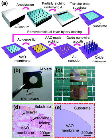 | ||
| Fig. 1 (a) Schematic illustration of the proposed process to fabricate sublithographic scale VLS nanowires by using attached AAO free-standing membrane mask. (b) Photography of AAO free-standing membrane (200 nm thickness). (c) Effect of hydrophilic surface treatment on the contact between AAO membrane and Si substrate. The upper sample is untreated, where some bright area can be seen due to the gap between AAO membrane and substrate. While the lower sample shows the good contact by hydrophilic surface treatment. (d) Optical microscope image of attached AAO membrane on Si substrate. Both membrane and substrate were not treated by oxygen plasma. Cracking and folding can be seen in the image. (e) Optical microscope image of attached AAO membrane on Si substrate. Both membrane and substrate were treated by oxygen plasma. | ||
Fig. 2(a) shows the SEM image of AAO membrane mask fabricated by the proposed method. The pitch between AAO pores is 63 nm, and the pore size is 20 nm. The AAO pores were highly uniform and regularly aligned as hexagonal form. The spatial regularity was also confirmed as fast Fourier transform (FFT) images as shown in the inset. Fig. 2(b)–(h) show the effects of AAO membrane thickness on the patterned arrays of Au catalysts and VLS grown MgO nanowires. MgO nanowires were grown on SrTiO3 (100) single crystalline substrate. Fig. 2(i) shows the XRD data. Most nanowires were epitaxially grown on SrTiO3 substrate. The SEM images show that increasing the thickness of the AAO membrane resulted in the spatial inhomogeneity of fabricated Au catalyst dots and VLS nanowires. The fabrication yield of nanowire per each pore was estimated and shown in Fig. 2(b). The fabrication yield was higher than 90% below the thickness of 200 nm, i.e. the aspect ratio of 10 in these membranes. The upper limitation of aspect ratio for metal depositions is due to a shadowing effect.27,28 Although the exact upper limitation depends on the straightness of the supplied flux to the substrate,19 Lei et al.15 have reported that the upper limitation of aspect ratio is about 10 even in well-controlled deposition configurations,27 which is clearly consistent with our results. Thus reducing a thickness of an attached AAO free-standing membrane mask is essential to realize VLS nanowires via AAO nanopores with a low aspect ratio.
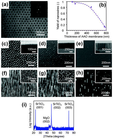 | ||
| Fig. 2 Effect of AAO membrane thickness on the growth of VLS nanowires. (a) FESEM image of AAO membrane mask with the pitch of 63 nm and the pore size of 20 nm. The inset shows an FFT image. (b) Relationship between the nanowire yield and the thickness of AAO membrane. (c–e) FESEM images of Au dot patterned by AAO membranes with the thicknesses of (c) 170 nm, (d) 500 nm and (e) 700 nm. Insets show the cross-sectional images of AAO membranes. (f–h) FESEM images of MgO nanowires grown on AAO membranes with the thickness of (f) 170 nm, (g) 500 nm and (h) 700 nm. Insets show top-view images. (i) Typical XRD data of patterned MgO nanowires. | ||
Fig. 3 shows the structural distribution data (the diameter and the length) of VLS nanowires fabricated by the above AAO membrane of 100 nm thickness. For comparison, the structural distribution data of nanowires fabricated by non-patterned catalysts are shown. Clearly the size distributions of nanowires by the attached AAO membrane mask method are much narrower than those of non-patterned samples. Quantitatively, in non-patterned samples, the standard deviations were 4.8 nm for the diameter and 275.3 nm for the length. Such wide distribution is due to the heterogeneous agglomeration of Au catalysts on the substrate surface in the absence of patterning during high temperature process.4,48 On the other hand, the standard deviations for AAO membrane assisted nanowires were greatly improved, 1.1 nm in the diameter, and 84.8 nm in the length. Note that the present nanowires of 18.5 nm average diameter with the standard deviation of 1.1 nm for large area had been hardly attainable using the existing attached AAO membrane mask methods. Here we discuss how the nanowires fabricated by AAO membrane exhibit the narrow distributions of the diameter and the length by employing the uniform size and spacing of catalyst array. Within the framework of VLS growth mechanism, the nanowire growth rate is determined by the flux of material supply per unit surface area of catalysts.46 Thus the size (area) distribution of catalysts on the substrate surface causes the spatial variation of nanowire growth rate by varying the local material supply rate per unit surface area of catalysts.46 Such catalyst size dependent nanowire growth rate has been also demonstrated.6,49,50 Thus the use of uniform-sized catalysts is essential not only for the uniformity of nanowire size but also for that of nanowire length. In addition to the catalyst size, a spacing between adjacent catalysts strongly affect the nanowire growth rate.46,51 This is because for nanowire growth, each catalyst collects diffusing adatoms from its surroundings and competes with adjacent catalysts for the material collection. In these phenomena, the uniformity of spacing between catalysts must play an important role on the competition of material transport into the catalysts. Thus the use of uniform spacing catalyst array is also crucial for uniform VLS nanowire growth.
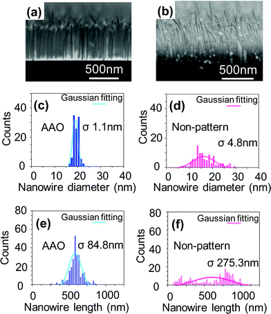 | ||
| Fig. 3 Comparison between AAO membrane method and non-patterned catalysts on the structural distributions of the diameter and the length. (a,b) FESEM images of MgO nanowires grown from (a) patterned catalysts by AAO membrane and (b) non-patterned catalysts. SrTiO3(100) substrate was used for the nanowire fabrications. The structural distribution analysis data in (c,d) the diameter and (e,f) the length of MgO nanowires for both patterned and non-patterned samples. | ||
Fig. 4(a)–(c) show the SEM images of AAO membranes when varying the pitch between pores. The pitches are of (a) 45 nm, (b) 63 nm and (c) 100 nm. Inset images show the near-edge of AAO membrane, and the thickness of AAO membrane was ∼100 nm. Fig. 4(d)–(f) show the SEM images of nanowires grown on SrTiO3 substrate by utilizing the spacing-controlled catalyst array. Insets show the FFT data calculated from the top-view images of the nanowires. In the SEM images, the spacing between nanowires seems to correspond to the spacing of AAO pores. More quantitatively, the ratio of AAO pitch to nanowire spacing was calculated and shown in Fig. 4(g). The ratio was found to be almost 1 for all samples, highlighting the feasibility of the present AAO method to control the spacing between nanowires. We attribute the successful spacing defining of nanowires due to a good contact between hydrophilic AAO membrane and hydrophilic substrate, which arises from a strong capillary interaction between them.
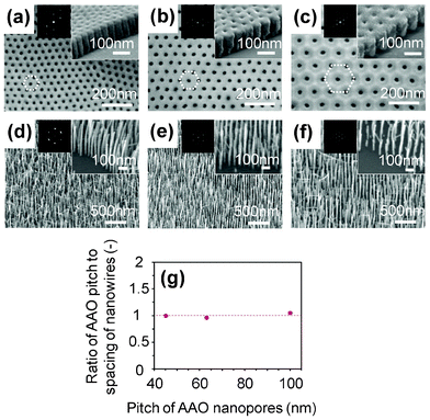 | ||
| Fig. 4 Controllability of spacing in AAO membrane method. FESEM images of (a–c) AAO membrane and (d–f) MgO nanowires grown on SrTiO3 substrate. The pitches of nanopore arrays are (a,d) 45 nm, (b,e) 63 nm and (c,f) 100 nm. Insets show FFT images projected by the FESEM images, and FESEM images at near-edge of AAO membrane. (g) Ratio of the pitch of AAO membrane and the spacing of fabricated MgO nanowire array. | ||
Fig. 5 demonstrates the applicability of the presented attached AAO membrane mask method for various substrates. SEM images and XRD data are shown in the figures. Nanowires were grown on various oxide substrates including MgO, LSAT and LaAlO3, whose lattice constants and surface chemical compositions are different.52 The pitches of pores and the thickness of AAO membrane were 63 nm and ∼100 nm, respectively. Well-defined nanowires can be grown on any oxide substrates by utilizing the present AAO method. This is because the present method does not require the specific surface chemical modifications to obtain the stuck contact between AAO membrane and substrate. It is noted that for a connected AAO membrane mask method, these highly insulative substrates require the use of electrochemically active electrode layers, for example Ta, Ti or W,27 which are detrimental for VLS nanowire growth with high temperature process up to 800 °C.36–47 Thus the present attached AAO process is a rather versatile method for VLS nanowire growths under various fabrication conditions.
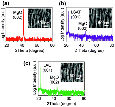 | ||
| Fig. 5 Feasibility of AAO membrane method for various substrates. (a–c) XRD scan data of MgO nanowire arrays patterned on various substrates. (a) Data of MgO substrate, (b) data of LSAT substrate, (c) data of LAO substrate. Insets show the titled FESEM images. | ||
Fig. 6 shows the scalability of the presented attached AAO membrane mask method. The photographic images were shown in the figures. The AAO membrane with 200 nm thickness was formed on a 3 inch Si substrate, and the membrane was not an open-through pore. The large scale AAO free-standing membranes can be seen in the images of Fig. 6(a) and (c), and the AAO membranes can be easily transferred onto the wafer without cracking or folding, as seen in Fig. 6(b) and (d). The feasibility of the AAO free-standing membrane for 4 inch scale is also shown in the Fig. 6(e). Note that the AAO free-standing membrane with 200 nm thickness for 4 inch scale is the largest so far reported. Thus the presented attached AAO membrane mask method is highly scalable, in principle this method can be further extended to a much larger scale substrate.
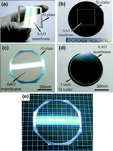 | ||
| Fig. 6 Scalability of AAO membrane method; (a) and (b) show the square-type AAO free-standing membrane with 200 nm thickness and the transferred membrane on the Si substrate; (c) and (d) show the circle-type AAO free-standing membrane with 200 nm thickness and the transferred membrane on the 3 inch Si wafer. (e) Shows 4 inch AAO free-standing membrane. | ||
Conclusion
In summary, we have successfully demonstrated a facile and scalable methodology to fabricate uniform-sized VLS nanowires at sublithographic scale by using ultra-thin AAO free-standing membrane created via a rigid Al frame and a hydrophilic contacting method. Use of the attached AAO free-standing membrane mask with the thickness less than 200 nm allows us to fabricate sub 20 nm nanowires with the standard deviations of 1.1 nm via defining the distributions of both the size and the spacing of the metal catalysts. We also show the scalability of the present attached AAO membrane mask method for a 4-inch scale wafer.Acknowledgements
This work was supported by NEXT. K. N. acknowledges the Sasakawa research program by the Japan Science Society. T. K. was supported by FIRST program.References
- D. R. Bowler, J. Phys.: Condens. Matter, 2004, 16, R721 CrossRef CAS.
- Y. Wu and P. Yang, J. Am. Chem. Soc., 2001, 123, 3165 CrossRef CAS.
- D. Wang, F. Qian, C. Yang, Z. Zhong and C. M. Lieber, Nano Lett., 2004, 4, 871 CrossRef CAS.
- D. L. Guo, X. Huang, G. Z. Xing, Z. Zhang, G. P. Li, M. He, H. Zhang, H. Y. Chen and T. Wu, Phys. Rev. B: Condens. Matter Mater. Phys., 2011, 83, 045403 CrossRef.
- I. Lombardi, A. I. Hochbaum, P. D. Yang, C. Carraro and R. Maboudian, Chem. Mater., 2006, 18, 988 CrossRef CAS.
- S. A. Dayeh and S. T. Picraux, Nano Lett., 2010, 10, 4032 CrossRef CAS.
- L. E. Jensen, M. T. Björk, S. Jeppesen, A. I. Persson, B. J. Ohlsson and L. Samuelson, Nano Lett., 2004, 4, 1961 CrossRef CAS.
- T. Kawano, M. Futagawa, Y. Arai, H. Takao and K. Sawada, Superlattices Microstruct., 2003, 34, 567 CrossRef.
- W. K. Choi, T. H. Liew, H. G. Chew, F. Zheng, C. V. Thompson, Y. Wang, M. H. Hong, X. D. Wang, L. Li and J. Yun, Small, 2008, 4, 330 CrossRef CAS.
- A. Pierret, M. Hocevar, S. L. Diedenhofen, R. E. Algra, E. Vlieg, E. C. Timmering, M. A. Verschuuren, G. W. G. Immink, M. A. Verheijen and E. P. A. M. Bakkers, Nanotechnology, 2010, 21, 065305 CrossRef.
- Y. S. Sastre, S. A. Dayeh, S. T. Picraux and C. A. Batt, ACS Nano, 2010, 4, 1209 CrossRef.
- X. X. Zhang, D. F. Liu, L. H. Zhang, W. L. Li, M. Gao, W. J. Ma, Y. Ren, Q. S. Zeng, Z. Q. Niu, W. Y. Zhou and S. S. Xie, J. Mater. Chem., 2009, 19, 962 RSC.
- H. Masuda and M. Satoh, Jpn. J. Appl. Phys., 1996, 35, L126 CAS.
- H. Masuda, K. Yasui and K. Nishio, Adv. Mater., 2000, 12, 1031 CrossRef CAS.
- M. H. Wu, L. Y. Wen, Y. Lei, S. Ostendorp, K. Chen and G. Wilde, Small, 2010, 6, 695 CrossRef CAS.
- M. S. Sander and L.S. Tan, Adv. Funct. Mater., 2003, 13, 393 CrossRef CAS.
- A. P. Li, F. Muller, A. Birner, K. Nielsch and U. Gösele, J. Appl. Phys., 1998, 84, 6023 CrossRef CAS.
- W. Lee, H. Han, A. Lotnyk, M. A. Schubert, S. Senz, M. Alexe, D. Hesse, S. Baik and U. Gösele, Nat. Nanotechnol., 2008, 3, 402 CrossRef CAS.
- X. L. Lu, Y. Kim, S. Goetze, X. G. Li, S. N. Dong, P. Werner, M. Alexe and D. Hesse, Nano Lett., 2011, 11, 3202 CrossRef CAS.
- T. Shimizu, T. Xie, J. Nishikawa, S. Shingubara, S. S. Senz and U. Gösele, Adv. Mater., 2007, 19, 917 CrossRef CAS.
- N. Kwon, N. Kim, J. Yeon, G. Yeom and I. Chung, J. Vac. Sci. Technol., B: Microelectron. Nanometer Struct.–Process., Meas., Phenom., 2011, 29, 031805 CrossRef.
- P. L. Chen, C. T. Kuo, F. M. Pan and T. G. Tsai, Appl. Phys. Lett., 2004, 84, 3888 CrossRef CAS.
- M. M. Crouse, A. E. Miller, D. T. Crouse and A. A. Ikram, J. Electrochem. Soc., 2002, 149, B321 CrossRef.
- Z. H. Wu, X. Y. Mei, D. Kim, M. Blumin and H. E. Ruda, Appl. Phys. Lett., 2002, 81, 5177 CrossRef CAS.
- H. Chik, J. Liang, S. G. Cloutier, N. Kouklin and J. M. Xu, Appl. Phys. Lett., 2004, 84, 3376 CrossRef CAS.
- L. Wen, Z. Shao, Y. Fang, K. M. Wong, Y. Lei, L. F. Bian and G. Wilde, Appl. Phys. Lett., 2010, 97, 053106 CrossRef.
- Y. Lei, W. P. Cai and G. Wilde, Prog. Mater. Sci., 2007, 52, 465 CrossRef CAS.
- I. Pastore, R. Poplausks, I. Apsite, I. Pastare, F. Lombardi and D. Erts, IOP Conf. Ser.: Mater. Sci. Eng., 2011, 23, 012025 CrossRef.
- H. J. Fan, P. Werner and M. Zacharias, Small, 2006, 2, 700 CrossRef CAS.
- H. Masuda and K. Fukuda, Science, 1995, 268, 1466 CAS.
- H. Masuda, M. Nagae, T. Morikawa and K. Nishio, Jpn. J. Appl. Phys., 2006, 45, L406 CrossRef CAS.
- X. Mei, D. Kim, H. E. Ruda and Q. X. Guo, Appl. Phys. Lett., 2002, 81, 361 CrossRef CAS.
- T. T. Xu, R. D. Piner and R. S. Ruoff, Langmuir, 2003, 19, 1443 CrossRef CAS.
- G. Q. Ding, M. J. Zheng, W. L. Xu and W. Z. Shen, Nanotechnology, 2005, 16, 1285 CrossRef CAS.
- D. F. Maclennan, J. Appl. Chem., 1959, 9, 519 CrossRef CAS.
- K. Nagashima, T. Yanagida, H. Tanaka and T. Kawai, J. Appl. Phys., 2007, 101, 124304 CrossRef.
- T. Yanagida, K. Nagashima, H. Tanaka and T. Kawai, Appl. Phys. Lett., 2007, 91, 061502 CrossRef.
- K. Nagashima, T. Yanagida, H. Tanaka, S. Seki, A. Saeki, S. Tagawa and T. Kawai, J. Am. Chem. Soc., 2008, 130, 5378 CrossRef CAS.
- T. Yanagida, A. Marcu, H. Matsui, K. Nagashima, K. Oka, K. Yokota, M. Taniguchi and T. Kawai, J. Phys. Chem. C, 2008, 112, 18923 CAS.
- K. Nagashima, T. Yanagida, K. Oka and T. Kawai, Appl. Phys. Lett., 2009, 94, 242902 CrossRef.
- K. Oka, T. Yanagida, K. Nagashima, H. Tanaka and T. Kawai, J. Am. Chem. Soc., 2009, 131, 3434 CrossRef CAS.
- A. Klamchuen, T. Yanagida, K. Nagashima, S. Seki, K. Oka, M. Taniguchi and T. Kawai, Appl. Phys. Lett., 2009, 95, 053105 CrossRef.
- K. Nagashima, T. Yanagida, K. Oka, M. Taniguchi, T. Kawai, J. S. Kim and B. H. Park, Nano Lett., 2010, 10, 1359 CrossRef CAS.
- K. Oka, T. Yanagida, K. Nagashima, T. Kawai, J. S. Kim and B. H. Park, J. Am. Chem. Soc., 2010, 132, 6634 CrossRef CAS.
- A. Klamchuen, T. Yanagida, M. Kanai, K. Nagashima, K. Oka, T. Kawai, M. Suzuki, Y. Hidaka and S. Kai, Appl. Phys. Lett., 2010, 97, 073114 CrossRef.
- A. Klamchuen, T. Yanagida, M. Kanai, K. Nagashima, K. Oka, S. Rahong, M. Gang, M. Horprathum, M. Suzuki, Y. Hidaka, S. Kai and T. Kawai, Appl. Phys. Lett., 2011, 99, 193105 CrossRef.
- K. Nagashima, K. T. Yanagida, K. Oka, M. Kanai, A. Klamchuen, J. S. Kim, B. H. Park and T. Kawai, Nano Lett., 2011, 11, 2114 CrossRef CAS.
- C. M. Müller, F. C. F. Mornaghini and R. Spolenak, Nanotechnology, 2008, 19, 485306 CrossRef.
- L. E. Fröberg, W. Seifert and J. Johansson, Phys. Rev. B: Condens. Matter Mater. Phys., 2007, 76, 153401 CrossRef.
- J. Kikkawa, Y. Ohno and S. Takeda, Appl. Phys. Lett., 2005, 86, 123109 CrossRef.
- M. T. Borgström, G. Immink, B. Ketelaars, R. Algra and E. P. A. M. Bakkers, Nat. Nanotechnol., 2007, 2, 541 CrossRef.
- Q. Li, W. Si and I. K. Dimitrov, Rep. Prog. Phys., 2011, 74, 124510 CrossRef.
| This journal is © The Royal Society of Chemistry 2012 |