Facile formation of nanostructured 1D and 2D arrays of CuO islands
PilHo
Huh
*a,
JungYup
Yang
a and
Seong-Cheol
Kim
*b
aSamsung SDI Co., Ltd., San #24 Nongseo-Dong, Giheung-Gu, Yongin-City, Gyeonggi-Do 446-711, Korea. E-mail: pilho.huh@samsung.com; jungyup.yang@samsung.com
bSchool of Textiles, Yeungnam University, Gyeungsan, Gyeungbuk 712-749, South Korea. E-mail: sckim07@ynu.ac.kr; Fax: 82538104684; Tel: 82538102787
First published on 18th April 2012
Abstract
Periodic one (1D) and two dimensional (2D) arrays of copper(II) oxide (CuO) islands were successfully created by simple heat treatment of spin-coated copper acetate–polyvinyl alcohol (PVA) composites on 1D and 2D surface relief grating (SRG) templates using photodynamic polymers. Formation of CuO islands can be explained as the successive collapse phenomenon of the grating (or groove) of the SRG template used. A scanning electron microscopy study reveals that the combination of a photodynamic polymer and copper acetate–PVA based on pyrolyzing led to directed self-assembly of metal oxide to form the arrays of CuO islands.
Inorganic micro- or nanostructures with well-defined shapes have been continuously developed due to their morphology-dependent properties and potential applications.1–4 Elaborate nanostructures have been fabricated through pattern-guided growth of inorganic materials5 and substrate-induced growth of inorganic minerals.6 Copper(II) oxide (CuO) has been extensively studied as a material with interesting electrochemical and catalytic properties.7–9 In addition, CuO is attracting great interest as a prospective candidate for a low-cost photovoltaic power generator because it is a p-type semiconductor with an indirect band-gap of ∼1.2 eV and it has a high optical absorption coefficient.10 Particularly, CuO nanostructures may function as a superconductor in high temperature,11 in lithium ion batteries,12 as an electron field emission source,13–15 and as an active layer in solid state solar cells due to their photoconductive and photochemical properties. CuO nanostructures may be either generated through oxidation of pure copper or formed through reduction of Cu2+. Some methods including template interface reaction,16 wet chemical methods,17,18 thermal decomposition,19 and electrospinning20 have been used to prepare well-defined CuO nanostructures. To the best of our knowledge, however, there are few reports of the fabrication and characterization of nanostructured CuO arrays.
In this study, CuO nanostructures with various dimensions were easily formed by pyrolyzing on the basis of SRG polymeric templates and copper acetate–polyvinyl alcohol (PVA) composites. The controlled shapes of CuO nanostructures were of periodic one (1D) and two dimensional (2D) arrays of CuO islands. This approach may be usefully developed as one means for creating an array of CuO islands with high density, because the arrangement of high density CuO islands could also enhance the efficiency of photoconductivity and photoactivity. The formation mechanism for well-aligned arrays of CuO islands is also discussed preliminarily.
In the experiments, all reagents were analytic grade and purchased from Sigma-Aldrich. They were used without further purification. In the procedure for fabricating CuO nanostructures, 10 g of Cu (CH3COO)2·H2O was dissolved in 20 g of de-ionized water and highly concentrated copper acetate solution was obtained after stirring for an hour. 30 g aqueous 20 wt% PVA (Mn = 120![[thin space (1/6-em)]](https://www.rsc.org/images/entities/char_2009.gif) 000) was added slowly into the copper acetate solution and then reacted until the transparent copper acetate–PVA composites were altered to green in a 60 °C temperature bath for 3 h. A transparent copper acetate–PVA solution was obtained through filtration into a syringe with a 0.45 μm membrane.
000) was added slowly into the copper acetate solution and then reacted until the transparent copper acetate–PVA composites were altered to green in a 60 °C temperature bath for 3 h. A transparent copper acetate–PVA solution was obtained through filtration into a syringe with a 0.45 μm membrane.
Poly (disperse orange 3) (PDO3) used in this work was prepared with a diglycidyl ether of bisphenol A, aniline, and 4-nitroaniline using a post azo-coupling reaction as described previously.21,22 Large-area microstructured 1D and 2D surface relief gratings (SRGs) for polymeric templates were prepared by a single-step holographic patterning process as reported previously.23
Scheme 1 shows the schematic process for creating the 1D and 2D arrays of CuO islands. 1D and 2D arrays of CuO islands were characterized by atomic force microscopy (AFM), scanning electron microscopy (SEM), and energy dispersive spectrometry for morphology and chemical composition. Optical behaviors were recorded using UV absorption spectroscopy in the wavelength range 200–1000 nm and photoluminescence (PL) spectroscopic techniques at an exciting wavelength of 399 nm.
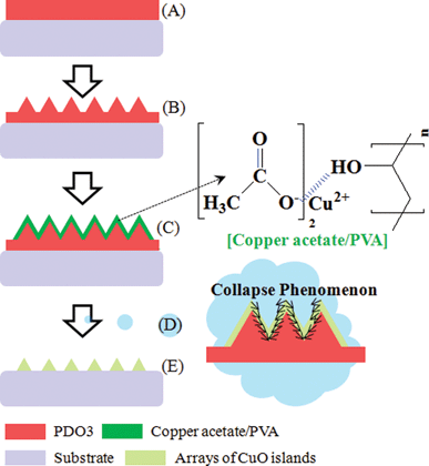 | ||
| Scheme 1 Schematic outline of the procedure used to create the 1D and 2D arrays of CuO islands: (A) the spin-coating of PDO3 film; (B) the inscribing of SRG using two coherent interfering laser beams; (C) the spin-coating of copper acetate–PVA composites on SRG; (D) collapse phenomenon of SRG and copper acetate–PVA toward SRG groove; (E) the formation of 1D and 2D arrays of CuO islands. | ||
Fig. 1 shows AFM and SEM images of nanostructured1D CuO arrays. As shown in Fig. 1A, AFM images reveal that 1D CuO arrays have a grating space of around 700 nm. A surface modulation depth of about 600 nm is also observed. Interestingly, SEM images of Fig. 1B clearly show that the resultant 1D CuO arrays are composed of slightly-dense CuO islands with a typical thickness of around 50–100 nm, and the period of a single array is approximately 1.0 μm. It can be seen that 1D array structures of CuO islands were self-organized through the heat treatment of copper acetate–PVA composites deposited on a 1D SRG polymeric template. The formation mechanism for periodic arrays of CuO islands can be explained as the successive collapse of gratings (or grooves) onto 1D SRG and copper acetate–PVA deposited on the surface of gratings (or grooves) of 1D SRG template as shown in Scheme 1. The oxidation of copper acetate–PVA composites or the calcination of an acetate–PVA complex may be attributed to the transition from Cu2+ to CuO.
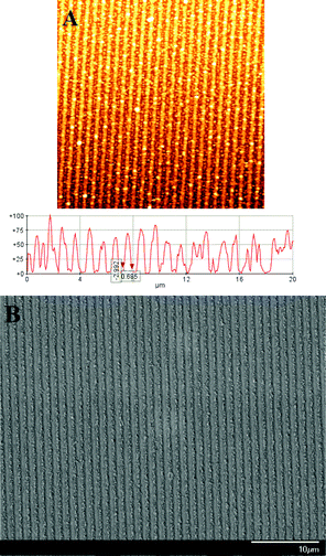 | ||
| Fig. 1 AFM and SEM images of 1D arrays of CuO islands created by the collapse phenomenon of heat treatment. | ||
The morphology of nanostructured 2D CuO arrays was analyzed by SEM images shown in Fig. 2. The lower magnification image in Fig. 2A indicates that the obtained 2D nanostructures are well-defined grid patterns comprised of groups of CuO islands. The diameter of CuO nanoparticles is on average 50–100 nm, while the grating spacing of 2D arrays is about 0.5 μm. The high magnification SEM images clearly show that CuO nanoparticles are densely packed to the center of grid patterns (shown in Fig. 2B and 2C). The formation mechanism of unique 2D CuO grid patterns can also be explained as the above-mentioned successive collapse phenomenon of 2D SRG template and copper acetate–PVA deposited onto the gratings (or grooves) of 2D SRG.
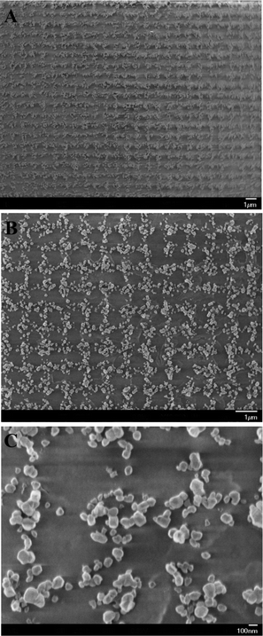 | ||
| Fig. 2 SEM images of 2D arrays of CuO islands comprised of CuO particles. | ||
An energy-dispersive analysis of X-ray (EDAX) spectrum used to identify the chemical composition of the resulting CuO nanostructures is shown in Fig. 3A. A characteristic peak of 8.06 keV can be seen at the Cu-Kα X-ray line. A characteristic peak for the OKα X-ray line is also observed at 0.51 keV. The results imply that CuO nanostructures were successfully gained through thermal oxidation of copper acetate–PVA film. Fig. 3B shows the UV-vis absorption spectrum of nanostructured CuO arrays. The optical absorption band edge is observed at around 940 nm. The band-gap energy (Eg) is obtained using the Kubelka–Munk function.
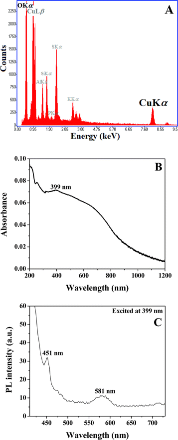 | ||
| Fig. 3 EDAX (A), UV-vis absorption (B), and photoluminescence (C) spectra of well-aligned CuO nanostructures. | ||
| E = 1239.6/l (eV) |
The structure of the produced CuO islands was characterized by X-ray diffraction (XRD). The XRD pattern of the as-prepared CuO arrays is shown in Fig. 4. The XRD peaks at 2θ values of 32.55°, 35.51°, 38.70°, 48.91°, 53.58°, and 58.41° correspond well to the characteristic diffractions of (110), (002,![[1 with combining macron]](https://www.rsc.org/images/entities/char_0031_0304.gif) 11), (111, 200), (
11), (111, 200), (![[2 with combining macron]](https://www.rsc.org/images/entities/char_0032_0304.gif) 02), (020), and (202) of crystalline copper oxide, respectively, which are consistent with the data of the JCPDS file (JCPDS file No. 05-661). The XRD patterns exhibit two main signals at 35.51° and 38.70° 2θ that can be ascribed to the (11) and (111) reflections of the CuO phase.28 This result indicated clearly that the final product is CuO.
02), (020), and (202) of crystalline copper oxide, respectively, which are consistent with the data of the JCPDS file (JCPDS file No. 05-661). The XRD patterns exhibit two main signals at 35.51° and 38.70° 2θ that can be ascribed to the (11) and (111) reflections of the CuO phase.28 This result indicated clearly that the final product is CuO.
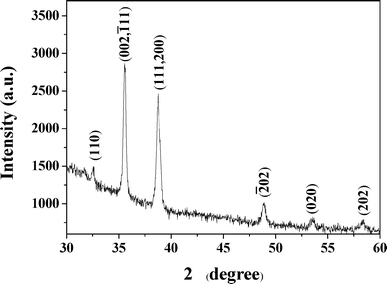 | ||
| Fig. 4 A representative XRD pattern for nanostructures of CuO islands formed after calcining at 500 °C. | ||
Conclusions
In summary, well-defined 1D and 2D arrays of CuO islands were successfully prepared using a photodynamic polymer for SRG polymeric templates and the thermal-oxidation of copper acetate–PVA composites spin-coated on them. The successive collapse phenomenon of gratings (or grooves) on SRG templates led to the formation of the self-organized CuO arrays comprised of CuO islands. Considering the simple method to fabricate 1D and 2D CuO nanostructures, well-ordered CuO nanostructures may be significantly utilized in the potential applications of photochemical, photoconductive devices, and chemo sensors.References
- Q. Ahsanulhaq, H. J. Kim and B. Y. Hahn, Nanotechnology, 2007, 18, 485307 CrossRef.
- X. Gou, G. Wang, J. Yang, J. Park and D. Wexler, J. Mater. Chem., 2008, 18, 965 RSC.
- G. Zou, H. Li, D. Zhang, K. Xiong, C. Dong and Y. Qian, J. Phys. Chem. B, 2006, 110, 1632 CrossRef CAS.
- K. N. Reddy, Q. Ahsanulhaq, H. J. Kim and B. Y. Hahn, Nanotechnology, 2007, 18, 445710 CrossRef.
- J.-H. Zhu, J.-M. Song, S.-H. Yu, W.-Q. Zhang and J.-X. Shi, CrystEngComm, 2009, 11, 539 RSC.
- J.-H. Zhu, S.-H. Yu, A.-W. Xu and H. Cölfen, Chem. Commun., 2009, 1106 RSC.
- J. A. Switzer, H. M. Kothari, P. Poizot, S. Nakanishi and E. W. Bohannan, Nature, 2003, 425, 490 CrossRef CAS.
- K. Nagase, Y. Zheng, Y. Kodama and J. Kakuta, J. Catal., 1999, 187, 123 CrossRef CAS.
- E. Barrera-Calva, J. Méndez-Vivar, M. Ortega-López, L. Huerta-Arcos, J. Morales-Corona and R. Olayo-Gonźalez, Research Letters in Materials Science, 2008, 2008, 5 CrossRef.
- S. Anandan, X. Wen and S. Yang, Mater. Chem. Phys., 2005, 93, 35 CrossRef CAS.
- X. G. Zheng, C. N. Xu, Y. Tomokiyo, E. Tanaka, H. Yamada and Y. Soejima, Phys. Rev. Lett., 2000, 85, 5170 CrossRef CAS.
- X. P. Gao, J. L. Bao, G. L. Pan, H. Y. Zhu, P. X. Huang and F. Wu, J. Phys. Chem. B, 2004, 108, 5547 CrossRef CAS.
- Y. W. Zhu, T. Yu, F. C. Cheong, X. J. Xu, C. T. Lim and V. B. C. Tan, Nanotechnology, 2005, 16, 88 CrossRef CAS.
- C. T. Hsieh and J. M. Chen, Appl. Phys. Lett., 2003, 82, 3316 CrossRef CAS.
- C. T. Hsieh, J. M. Chen, H. H. Lin and H. C. Shih, Appl. Phys. Lett., 2003, 83, 3383 CrossRef CAS.
- Z. S. Hong, Y. Cao and J. F. Deng, Mater. Lett., 2002, 52, 34 CrossRef CAS.
- W. Wang, Z. Liu, Y. Liu, C. Xu, C. Zheng and G. Wang, Appl. Phys. A: Mater. Sci. Process., 2003, 76, 417 CrossRef CAS.
- H. Q. Wu, X. W. Wei, W. M. Shao, J. S. Gu and M. Z. Qu, Chem. Phys. Lett., 2002, 364, 152 CrossRef CAS.
- C. Xu, Y. Liu, G. Xu and G. Wang, Mater. Res. Bull., 2002, 37, 2365 CrossRef CAS.
- H. Wu, D. D. Lin and W. Pan, Appl. Phys. Lett., 2006, 89, 1331251 Search PubMed.
- X. Wang, J. Kumar, S. K. Tripathy, L. Li, J-I. Chen and S. Marturunkakul, Macromolecules, 1997, 30, 219 CrossRef CAS.
- S-S. Kim, C. Chun, J-C. Hong and D-Y. Kim, J. Mater. Chem., 2006, 16, 370 RSC.
- D. Y. Kim, L. Li, X. L. Jiang, V. Shivshankar, J. Kumar and S. K. Tripathy, Macromolecules, 1995, 28, 8835 CrossRef CAS.
- J. A. Switzer, H. M. Kothari, P. Poizot, S. Nakanishi and E. W. Bohannan, Nature, 2003, 425, 490 CrossRef CAS.
- R. S. Ningthoujam, N. S. Gajbhiye, A. Ahmed, S. S. Umre and S. J. Sharma, J. Nanosci. Nanotechnol., 2008, 8, 3059 CrossRef CAS.
- A. S. Lanje, S. J. Shrama, R. B. Pode and R. S. Ningthoujam, Arch. Appl. Sci. Res., 2010, 2, 127 CAS.
- A. S. Lanje, S. J. Shrama and R. B. Pode, Arch. Phy. Res., 2010, 1, 49 CAS.
- ICDD card no. 45-937.
| This journal is © The Royal Society of Chemistry 2012 |