Printed conductive features for DNA chip applications prepared on PET without sintering†
Albert R.
Liberski
abc,
Joseph T.
Delaney
Jr.
abc,
Aleksandra
Liberska
ab,
Jolke
Perelaer
abc,
Martha
Schwarz
de,
Thomas
Schüler
de,
Robert
Möller
de and
Ulrich S.
Schubert
*abc
aLaboratory of Organic and Macromolecular Chemistry (IOMC), Friedrich-Schiller-University Jena, Humboldtstraße, 10, 07743, Jena, Germany
bJena Center for Soft Matter (JCSM), Friedrich-Schiller-University Jena, Humboldtstraße, 10, 07743, Jena, Germany
cDutch Polymer Institute (DPI), P.O. Box, 902, 5600, AX Eindhoven, The Netherlands. E-mail: ulrich.schubert@uni-jena.de
dInstitute of Physical Chemistry, Friedrich-Schiller-University Jena, Helmholtzweg, 4, 07743, Jena, Germany
eInstitute of Photonic Technology, Albert Einstein Straße, 9, 07745, Jena, Germany
First published on 20th January 2012
Abstract
We present here an innovative and cheap alternative for the preparation of conductive tracks printed on flexible polymer substrates at room temperature. For this purpose, we applied a combination of a Tollens reagent-based silver deposition and printed mask, using an office laser printer. The as-prepared conductive structures were used for DNA chip fabrication. The great advantage of the presented method is that the conductive features can be fabricated in a facile and inexpensive way, while maintaining the high flexibility to tailor the design to its application. The DNA chips showed the same response as well as sensitivity compared to chips made conventionally by photolithography or screen printing.
Introduction
Flexible electronics combine bendable substrates together with inorganic materials by means of printing technologies, enabling light-weight and extremely cost-efficient electronic systems. Prevalent market drivers include organic photovoltaics,1 electro-optic devices and displays,2 logic and memory components,3 as well paper-based batteries4 and radio frequency identification tags.5 In the near future, a highly viable and innovative fusion of three technological areas—microelectronics, chemistry and printing—is foreseen, which will create markets with annual revenues estimated at more than €200 billion.6Currently, the main method to fabricate conductive features on a rigid substrate is photolithography. Photolithography offers superior resolution as well as repeatability; at present, the industrial state-of-the-art feature size is 32 nm, at mass production and on 300 mm wafers.7 However, photolithography is not a flexible fabrication technique, since each deposition of electrically conductive material requires a pre-designed mask. Changing the design requires the fabrication of a new mask for each design, increasing production time, and thereby costs, significantly. As a result, the process cannot be easily applied to rapidly changing demands. In workflows requiring a diverse range of circuit patterns to be fabricated on demand, such as in a basic research and development environment, this is a very significant limitation.
Alternatively, inkjet printing of metal precursor inks, such as those based on silver nanoparticles or metal–organic complexes, has proven to be a versatile and comparatively inexpensive method to create interconnects and contacts.8,9 Inkjet printing is an advanced dispensing technique that produces on-demand sub-nanolitre droplets with great precision, and is capable of patterning substrates in a selective manner. However, the application of inkjet fabrication methods are as yet precluded for many mass-production processes, since a post-treatment, referred to as ‘sintering’, is necessary to convert the printed metal precursor feature into a functional, electrically conductive structure.10 Although much effort has been invested in the last years to decrease the sintering temperature by tailoring the precursor inks or application of alternative sintering techniques,11,12 a fast and reliable method to produce highly conductive features on large areas has still not been found. Moreover, the temperature requirements for sintering limit the application of inkjet printing to the substrates that are process-capable, and exclude many otherwise desirable, inexpensive, flexible substrates, such as paper and low melting polymers.
Hohnholz et al. reported the use of an office laser printer to print the toner ink on specific locations to create a local difference in surface energy of the substrate.13 The surface was then coated with the conducting polymer poly(3,4-ethylenedioxythiophene):poly(4-styrene sulfonate) (PEDOT:PSS) and as a result of the pre-patterning, only the hydrophilic parts are covered with the conductive aqueous ink. The printed toner material is removed by washing with toluene and the resulting product was used as the basis for a liquid crystal display with push-button arrays.
Besides the aforementioned applications for circuit boards and electrode structures there are also other applications that would greatly benefit from inexpensive and flexible production strategies. One of those possible applications would be chip-based electrical or electrochemical detection of biomolecules and their interactions. The requirements for chip-based detection systems are: preferably low costs, the possibility for the detection of a variety of molecules at the same time (parallel and high-throughput) and only little sample volumes, offering ideally higher selectivity and greater sensitivity. The rise of interest in recent years of lab-on-paper approaches to rapid prototyping and test development illustrates the attractiveness of this philosophy.
The state-of-the-art for the detection of biomolecules is the readout of the biochips via optical detection schemes—the majority of which rely on the detection of fluorescence signals. In recent years, however, alternative concepts which renounce the use of optics have been described.14 One of these detection schemes is the electrical readout of biochips.15 There are two major advantages of electrical readout over the established optical methods for biochip analysis. Firstly, the optical systems commonly used are highly delicate systems, which can be easily damaged without care, while electrical readout systems are comparatively robust, and offer the prospect of facile miniaturization. Secondly, the optical systems used, as well as the fluorescent dyes themselves, are often expensive; by contrast, electrical readout devices are inexpensive and ubiquitous. Furthermore, the latter method is independent of the used chip substrate.
The usage of polymer foils is also favored, since the foils are easy to handle and cheaper than glass or silicon substrates. On a bench scale, they are also easier to tailor to the desired shape and size. The electrical readout methods have been demonstrated on silicon and polymer substrates with electrode structures made by photolithography as well as on glass substrates with screen printed electrodes.16,17 These experiments have successfully demonstrated the use of the electrical detection scheme for the detection of biomolecules with high reproducibility. Biochips, also known as microarrays, are robust and small substrates, on which a high number of biological and biochemical tests can be performed quickly and accurately. They have enormous capacity (for example, an examination of the entire human genome in a single experiment) and offer the possibility for a miniaturized, parallelized, and automated on-site application.18 Based on the substances to be tested and the readout requirements, the shape and layout of the microarray can be designed accordingly.
As probe analytes, DNA (oligonucleotides, cDNA, etc.), proteins,19 peptides,20 and whole cells21 have been used. The concept of the Southern blot was used in the development and the creation of microarrays,22 and as a result a solid phase-based analysis of labelled oligonucleotides was made possible for the first time.23 A rapid technological development took place in the early 90′s,24 where the first commercially available DNA chip (HIV-Gene-chip) was manufactured by Affymetrix and was introduced to the market in 1994.25 Biochips may be produced with advanced manufacturing processes. The standard readout for biochips is the detection of a fluorescence signal. However, in the last years alternative readout methods have been described that would enable the construction of small, robust and cost-efficient readout devices for point-of-care applications. One of those new readout technologies is the electrical readout of biochips;25 for this application, electrode structures are required, which are usually produced by either photolithography or screen printing.
Here, we report an innovative and cheap method to produce highly conductive features at room temperature on flexible polymer substrates, applied in the production of DNA chip prototypes. Our method uses neither metal precursor inks, nor a sintering step at high temperature, which we think provides significant reduction of the production costs. Instead, the process we developed involves electroless chemical deposition of a thin layer of nanostructured metallic silver onto a thin polyester foil (in practice, an ordinary office transparency sheet), which is subsequently used as the substrate for printing.
Experimental
Materials & chemicals
Silver trifluoromethanesulfonate (Cat. No. AB112072) was purchased from ABCR (Karlsruhe, Germany). Black toner (Cat. NO. Q595OA) was purchased from Hewlett-Packard Company (CA, USA). A4 laser and copier transparencies (210 × 297 mm) and Scotch tape were received from Supplies Team (West Yorkshire UK). Ammonium hydroxide (25 wt-% aqueous solution) was purchased from Carl-Roth (Karlsruhe, Germany). Fructose (Cat.NO. F0127-500G) was purchased from Sigma-Aldrich (St. Louis, MO, USA).Preparation of the silver layer
Standard office transparency sheets (A4, PET) are placed onto a sheet of aluminum foil and the edges of the PET foil are fixed to the aluminum foil using scotch tape; this is to prevent any liquid flowing between the aluminum and PET foils. Next, the edges of the aluminum foil are bent up, to prevent liquids from flowing off of the PET (see Supplementary Information Fig. 1†). Then, 100 mL of a 20 wt% water solution of fructose was dispensed onto the PET foil. A mixture of 0.5 g silver triflate and 0.6 mL of 25 wt% ammonium hydroxide was filtrated and added dropwise uniformly onto the PET using a pipette (see Supplementary Information Fig. 1†). After 3 h, the fructose solution was removed and the PET foil was submerged in water. The foil was then washed by gently shaking underwater back-and-forth for 10 min and dried using a nitrogen stream.Preparation of the conductive features
The as-prepared PET foil with the deposited silver layer was placed in the paper reservoir of an office laser printer (HP Color LaserJet 4700 dn, Hewlett-Packard Company (CA, USA)). The designed layout was then printed in black-and-white mode, using only the black toner (Q595OA) (see Fig. 1). The obtained printed foil was subsequently heated for 30 s at 110 °C, after which the excess of silver was removed using ethanol and a paper tissue. Finally, the circuitry design was cut out to its final shape.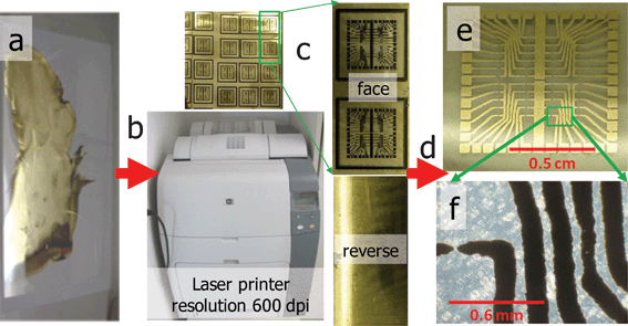 | ||
| Fig. 1 Workflow for the fabrication of conductive features: (a) transparency coated with a silver nanoparticle layer, (b) printing a circuitry layout using a standard office laser printer, (c) images of the obverse and reverse sides of the printout, (d) removal of excesses silver using ethanol-soaked paper tissue, (e) final conductive patterns layout as viewed through the reverse side of the transparency, (f) bright field microscopy image of individual lines of silver covered with black toner material. | ||
DNA chip preparation
As previously mentioned, the circuitry design on the PET foil was pre-cleaned in distilled water for 10 min (gently shaken) and dried under nitrogen. Next, single stranded DNA (5′-TTT TTT CAG CAT GTG CTC CTT GAT TCT ATG-3′, Amino C6 on 5′) was manually spotted in different concentrations as well as different sequences for one mismatch (5′-TTT TTT CAG CAT GGG CTC CTT GAT TCT ATG-3′, amino-modified on 5′) and three mismatches (5′-TTT TTT CAG CAT TAT CTC CTT GAT TCT ATG-3′, amino-modified on 5′). A spotting buffer containing 10 wt-% glycerin and 5× phosphate buffered saline (PBS) buffer was used to ensure a homogeneous spot coverage. To assure the coverage of every electrode gap, 15 drops per spot (15 × 0.4 nL = 6 nL) were applied to larger spots.The prepared DNA chip was subsequently incubated overnight at 37 °C in a humidity chamber. Afterwards, the DNA spots on the foil were allowed to dry and then exposed for 10 min to UV light (254 nm), followed by 10 min washing in 0.1× saline-sodium citrate (SSC) buffer/0.5% sodium dodecyl sulphate (SDS).
After the immobilization of the capture DNA on the PET foil, the hybridization of biotin labeled target DNA was performed. For this, a 500 nM target DNA solution (B150 - 5′-CAT AGA ATC AAG GAG CAC ATG CTG AAA AAA-3′, Biotin marked) was used at 40 °C in 2× SSC/0.1% SDS for 1 h. Subsequently, the foil was washed for 5 min in 2× SSC/0.1% SDS, 5 min in 2× SSC and finally 5 min in 0.2× SSC. The binding of the enzyme horseradish peroxidise (HRP) 1![[thin space (1/6-em)]](https://www.rsc.org/images/entities/char_2009.gif) :1000 in PBST (1× PBS/0.05% Tween20) allows a final enzyme induced silver deposition, followed by washing 3 × 5 min with 1× PBST and shortly with distilled water, to remove any remaining chloride. An enzyme-controlled silver deposition is then applied to bridge the electrodes, using EnzMet™ reagent (Nanoprobes, Yaphank, NY). The reaction was stopped with water and the foil was dried under nitrogen.
:1000 in PBST (1× PBS/0.05% Tween20) allows a final enzyme induced silver deposition, followed by washing 3 × 5 min with 1× PBST and shortly with distilled water, to remove any remaining chloride. An enzyme-controlled silver deposition is then applied to bridge the electrodes, using EnzMet™ reagent (Nanoprobes, Yaphank, NY). The reaction was stopped with water and the foil was dried under nitrogen.
Characterization of silver paths
A part of the conductive silver layer was peeled off from a chip using standard office Scotch adhesive tape (Product No. 34-8509-3289-7, 3 M, St. Paul, MN, USA). The thickness as well as the cross-sectional area of the silver layer was measured using an optical profilometer (Wyko NT9100, Veeco, Tucson, USA, 2.5× magnification, coupled with a 2.0× FOV). Field emission scanning electron microscopy (FE-SEM) images were taken using a JEOL JSM-6700F (Tokyo, Japan).The electrical resistance ρ of the patterns was calculated from the resistance R, the length l, and the cross sectional area A of the line, using the formula ρ = R·A/l. The resistance was measured over 1.0 cm, and was found to be 6.0 ± 0.2 Ω using a multimeter (Voltcraft Plus VC 960, Conrad, Germany). The calculated resistivity was found to be 4.4 μΩ·cm, which is approximately 2 to 3 times the value for bulk silver (1.59 μΩ·cm).8
After enzymatic silver deposition, the conductance was measured independently in three separate experiments, carried out using three chips that were prepared in three separate printouts. Within the chip, the spot contained the same formulation of reagents and the spot was printed three times to yield in total 9 readouts (3 times 3 chips) for each analytical event: positive control, negative control, complementary DNA, 1 and 3 mismatches. The data collected from 3 different chips revealed a small standard deviation (see Fig. 4).
Results and discussion
In contrast to photolithography, where rigid substrates with fixed dimensions are used, printing opens the possibility to a much broader selection of substrates. From a processability standpoint, flexible polymer substrates have a number of comparative advantages over rigid counterparts, since they can be readily bent and cut in all desired shapes. Moreover, polymer substrates are mechanical resistive as well as transparent. Many photolithographic processes, however, involve aggressive chemicals, such as strong acids, which may preclude substrates and processing sequences that are otherwise compatible. In the workflow, shown in Fig. 1, only ethanol is required for the removal of excess silver nanoparticles. Furthermore, the expensive lithography instruments are here replaced by cheaper laser printers that are available in the majority of modern offices.One of the challenges was identifying an efficient method for depositing a conductive silver layer without the need for sintering. There are numerous examples in the literature that describe the preparation of conductive features by using nanoparticle ink that require a sintering step.8 In general, the higher the sintering temperature the lower the resulting resistivity will be. However, when using temperature sensitive polymer foils, the processing temperature is limited.
For almost 120 years,26 the Tollens reaction has been proven to be a perennially abundant source for new forms of electroless metallic silver, with an as-yet unexhausted-variety of possible morphologies.27 By changing the stoichiometry and the reaction conditions, and by the addition of soft templates, the growth of metallic silver can be guided to a specific goal.28 While there are numerous protocols for developing silver nanoparticles using the Tollens reaction for a diverse number of technical applications, the variety of publications investigating its use as an electroless, sinterless/low sintering temperature technique has remained somewhat limited until recently.
The objective was to utilize the Tollens reaction in a manner that would yield conductive printed structures without the need for sintering. For this purpose, we combined two reactive components: an aldehyde and a silver complex. For the aldehyde, fructose was chosen. The silver complex was diaminesilver trifluoro-methane-sulfonate, which was selected due to its attractive high solubility compared to other commercially available silver salts, with the logic being that it could be used in higher concentrated formulations later on (if required).
By using the Tollens reaction, described in more detail in the experimental section, a thin layer of silver nanoparticles was prepared on standard polyethylene terephthlate (PET) transparency sheets. The circuitry diagram is designed using standard drawing software on a personal computer, which is saved as a bitmap file. The silver coated transparency foil was subsequently placed in a laser printer, which was used to print the aforementioned circuitry layout directly onto the as-prepared silver layer. At this point, the toner coated silver layer was found to be well adhered to the transparency, but to ensure that the toner material was fully immobilized, the sample was heated for 30 s on a hotplate at 110 °C. The binding of the toner material was then found to be good, since the layer was observed to remain intact upon removing the excess of silver using ethanol and a paper tissue (see Supplementary Information Fig. 2†). This process yielded the final conductive features.
The characterization of conducting paths was performed using confocal interferometry, scanning electron microscopy (SEM) and resistance measurements, as well as imaging using low resolution bright light microscopy (Fig. 2).
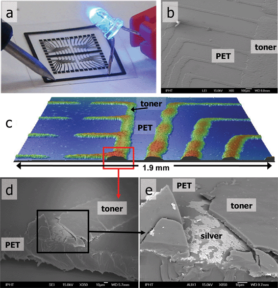 | ||
| Fig. 2 Circuitry layout printed on PET foil: (a) proof of conductivity (note: black layer of toner must be broken to reach the conductive silver—see Supplementary Information Fig. 2†), (b) scanning electron microscopy (SEM) image of toner coating silver, (c) 3D optical profilometry image of the patterns, (d) cross-sectional SEM of the conducting path, (e) conducting silver layer under the black toner material. | ||
The resistivity of the structures was found to be 4.4 μΩ·cm; a value that is approximately twice the corresponding value for bulk silver. For comparison, room temperature sintering of inkjet printed silver nanoparticles has been reported by Magdassi et al. recently.29 They obtained features with a resistivity of 5× the bulk silver value without heating. While a lower resistivity can be obtained by using a high temperature (>400 °C).10 This approach is not compatible with temperature sensitive polymer foils, like PET. The feature resolution of the resulting printed features is practically equal to the resolution of the laser printer, which in this case is 600 dpi, but could be readily improved by using a higher resolution laser printer.
The resulting prepared samples were used as the basis of a DNA chip, applying the strategy as described elsewhere in more detail.30 Briefly, the individual electrode gaps are modified with different capture molecules. After the binding of the complementary target molecules to the immobilized capture molecules, an enzyme is bound to the immobilized target molecules. The enzyme catalyses the deposition of silver that, as a consequence, bridges the electrode gap. This leads to a conductive path and hence the binding of target molecules can be detected by a simple electrical conductivity measurement (Fig. 3). For comparison, Supplementary Information Fig. 4† shows images of screen printed reference samples.
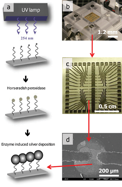 | ||
| Fig. 3 Working principles of a DNA chip: (a) scheme of the chip preparation and analysis, (b) DNA chip reader, (c) printed circuit board layout, (d) bridge between two electrode gaps due to the binding of complementary target molecules and enzyme catalyzed silver deposition. | ||
Besides electrochemical detection, the binding of complementary target DNA can also be measured optically. For the optical measurement images of the silver spots were taken and evaluated by measuring the resulting gray value, using the program ImageJ 1.40 (National Institute of Health, USA). After the determination of the gray values for the positive control, which is set as 100%, all other values are measured in proportion to this (Fig. 4). The convergence of the results obtained with the use of chips produced in separate cycles leads to the conclusion that the quality of the chips does not change between successive prints. Furthermore, the obtained results here were found to be similar, independent of the chip substrate and the production method for the electrode structures.16
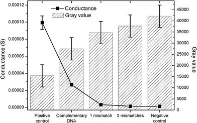 | ||
| Fig. 4 Comparison of optical and electrical measurements, showing the effect of hybridization efficiency/mismatching on the measured gray values and conductance. | ||
The thickness of the silver deposition depends on the complementary behavior and concentration of the target DNA. Therefore, the hybridization of complementary DNA results in a higher electrical conductivity than the measured conductivities for the mismatched probes (Fig. 4). The obtained results correlate also with the optical results showing a high gray value for the positive control and for the complementary DNA, corresponding to the highest degree of silver deposition as a result of the binding efficiency of the DNA. Samples that exhibit increased numbers of mismatches result in a lower binding efficiency and, consequently, a lower deposition of silver, as well as a decrease (increase) of the conductivity (gray) value. The negative control shows a very low conductance, as expected. These results demonstrate the successful transfer of the chip-based electrical DNA detection to the new substrates as the results are in good agreement with tests performed on glass substrates with screen printed electrodes.16 Hence, our approach can produce DNA chips in a fast and inexpensive manner, without the need for an expensive mask required for photolithography.
This method does not produce samples in a high quantity, as for example photolithography, but has the advantage of being highly flexible, enabling design tailoring for a particular application, such as chip-based DNA detection. With this in mind, our approach of chip production described here is not to compete with photolithographic techniques, where (hundreds of) thousands of identical samples can be prepared in a fast and cheap manner with an extreme high resolution (nanometer). Rather, the aim is to enable the production of a small number of samples, i.e. several dozens to a few hundred, while maintaining the high flexibility to tailor the design to its application, with minimal effort, and having a resolution in the micrometre range.
Conclusions
An innovative and alternative method was presented for the fabrication of disposable electrical circuitries on flexible polymer substrates for usage in DNA chips. We have used a modified Tollens reaction, where the aim was to prepare highly conductive features on simple, unmodified polymer substrates without the need for (high temperature) sintering and masks. Instead of using the expensive and comparatively inflexible lithography route, standard office laser printers were used to fabricate the mask layout. Laser printing has the advantage of being a maskless and digital technique, where one-of-a-kind circuit layouts can be easily programmed using standard drawing software and where layouts can be changed easily. The obtained resistivity was approximately twice that of bulk silver, which is usually obtained only via a high temperature sintering process. As a consequence, the usage of cheap polymer foils that require a low processing temperature, for example PET, is enabled.The flexible conductive features were successfully used in a chip-based DNA detection with electrical readout. Furthermore, the geometry of the chips as well as the number of electrodes per chip can be easily adapted using this flexible approach; hence allowing a rapid prototyping of different chip layouts for many applications with minimal cost and time requirements.
Acknowledgements
The authors would like to thank the Dutch Polymer Institute (Technology Area HTE) for financial support.References
- V. Shrotriya, Nat. Photonics, 2009, 3, 447 CrossRef CAS.
- H. M. Haverinen, R. A. Myllyla and G. E. Jabbour, J. Disp. Technol., 2010, 6, 87 CrossRef CAS.
- K. Song, D. Kim, X.-S. Li, T. Jun, Y. Jeong and J. Moon, J. Mater. Chem., 2009, 19, 8881 RSC.
- G. Nystrom, A. Razaq, M. Stromme, L. Nyholm and A. Mihranyan, Nano Lett., 2009, 9, 3635 CrossRef.
- D. Y. Shin, Y. Lee and C. H. Kim, Thin Solid Films, 2009, 517, 6112 CrossRef CAS.
- http://www.lope-c.com, Organic Electronics Association Last accessed: 20th October 2010.
- A. E. Grigorescu and C. W. Hagen, Nanotechnology, 2009, 20, 292001 CrossRef CAS.
- J. Perelaer, P. J. Smith, D. Mager, D. Soltman, S. K. Volkman, V. Subramanian, J. G. Korvink and U. S. Schubert, J. Mater. Chem., 2010, 20, 8446 RSC.
- E. Tekin, P. J. Smith and U. S. Schubert, Soft Matter, 2008, 4, 703 RSC.
- J. Perelaer, A. W. M. de Laat, C. E. Hendriks and U. S. Schubert, J. Mater. Chem., 2008, 18, 3209 RSC.
- J. Perelaer, M. Klokkenburg, C. E. Hendriks and U. S. Schubert, Adv. Mater., 2009, 21, 4830 CrossRef CAS.
- M. L. Allen, M. Aronniemi, T. Mattila, A. Alastalo, K. Ojanpera, M. Suhonen and H. Seppa, Nanotechnology, 2008, 19, 175201 CrossRef.
- D. Hohnholz, H. Okuzaki and A. G. MacDiarmid, Adv. Funct. Mater., 2005, 15, 51 CrossRef CAS.
- R. Möller, T. Schüler, S. Günther, M. R. Carlsohn, T. Munder and W. Fritzsche, Appl. Microbiol. Biotechnol., 2008, 77, 1181 CrossRef.
- M. Schena, D. Shalon, R. Heller, A. Chai, P. O. Brown and R. W. Davis, Proc. Natl. Acad. Sci. U. S. A., 1996, 93, 10614 CrossRef CAS.
- T. Schüler, R. Kretschmer, S. Jessing, M. Urban, W. Fritzsche, R. Möller and J. Popp, Biosens. Bioelectron., 2009, 25, 15 CrossRef.
- A. Brinker, H. Schulze, T. Bachmann and R. Möller, Eng. Life Sci., 2011, 11, 148 CrossRef.
- R. L. Stears, T. Martinsky and M. Schena, Nat. Med., 2003, 9, 140 CrossRef CAS.
- G. MacBeath and S. L. Schreiber, Science, 2000, 289, 1760 CAS.
- S. Fodor, J. Read, M. Pirrung, L. Stryer, A. Lu and D. Solas, Science, 1991, 251, 767 CAS.
- J. Ziauddin and D. M. Sabatini, Nature, 2001, 411, 107 CrossRef CAS.
- E. M. Southern, J. Mol. Biol., 1975, 98, 503 CrossRef CAS.
- G. Ramsay, Nat. Biotechnol., 1998, 16, 40 CrossRef CAS.
- A. Marshall and J. Hodgson, Nat. Biotechnol., 1998, 16, 27 CrossRef CAS.
- T. Schüler, T. Asmus, W. Fritzsche and R. Möller, Biosens. Bioelectron., 2009, 24, 2077 CrossRef.
- B. Tollens, Ber., 1881, 14, 1950 CrossRef.
- V. K. Sharma, R. A. Yngard and Y. Lin, Adv. Colloid Interface Sci., 2009, 145, 83 CrossRef CAS.
- F. Ni and T. M. Cotton, Anal. Chem., 1986, 58, 3159 CrossRef CAS.
- S. Magdassi, M. Grouchko, O. Berezin and A. Kamyshny, ACS Nano, 2010, 4, 1943 CrossRef CAS.
- R. Möller, R. D. Powell, J. F. Hainfeld and W. Fritzsche, Nano Lett., 2005, 5, 1475 CrossRef.
Footnote |
| † Electronic supplementary information (ESI) available. See DOI: 10.1039/c2ra01191c |
| This journal is © The Royal Society of Chemistry 2012 |