Graphene edges: a review of their fabrication and characterization
Xiaoting
Jia
a,
Jessica
Campos-Delgado
b,
Mauricio
Terrones
cd,
Vincent
Meunier
e and
Mildred S.
Dresselhaus
*f
aDepartment of Materials Science and Engineering, Massachusetts Institute of Technology, Cambridge, MA, USA. E-mail: xjia@mit.edu.; Tel: +617 253 6860
bDivisão de Metrologia de Materiais, Instituto Nacional de Metrologia, Normalização e Qualidade Industrial (INMETRO), Duque de Caxias, RJ, Brazil. E-mail: jessica.mex@gmail.com
cExotic Nanocarbon Research Center, Shinshu University, Wakasato 4-17-1, Nagano, Japan. E-mail: mtterrones@shinshu-u.ac.jp
dDepartment of Physics and Materials Research Institute, The Pennsylvania State University, 104 Davey Lab., University Park, PA 16802–6300, USA. E-mail: mut11@psu.edu; mtterrones@gmail.com
eDepartment of Physics, Applied Physics, and Astronomy, Rensselaer Polytechnic Institute, Troy, NY, USA. E-mail: meuniv@rpi.edu
fDepartment of Physics and Department of Electrical Engineering and Computer Science, Massachusetts Institute of Technology, Cambridge, MA, USA. E-mail: millie@mgm.mit.edu
First published on 22nd November 2010
Abstract
The current status of graphene edge fabrication and characterization is reviewed in detail. We first compare different fabrication methods, including the chemical vapor deposition method, various ways of unzipping carbon nanotubes, and lithographic methods. We then summarize the different edge/ribbon structures that have been produced experimentally or predicted theoretically. We discuss different characterization tools, such as transmission electron microscopy and Raman spectroscopy, that are currently used for evaluating the edge quality as well as the atomic structures. Finally, a detailed discussion of defective and folded edges is also presented. Considering the short history of graphene edge research, the progress has been impressive, and many further advances in this field are anticipated.
 Xiaoting Jia | Xiaoting Jia was born in Dongyang, Zhejiang province, China. She received a B.S. degree in Materials Science from Fudan University, China in 2004, and a M.S. degree in Materials Science and Engineering from Stony Brook University in 2006. She is currently a PhD candidate in the Department of Materials Science and Engineering at Massachusetts Institute of Technology. Her research interests are focused on the in-situ TEM studies of thermoelectric nanomaterials, quantum dots, and carbon-based nanostructures including carbon nanotubes, graphene, and graphitic nanoribbons, and also on the STM studies of graphene and graphene edges. |
 Jessica Campos-Delgado | Jessica Rosaura Campos Delgado received her B.S. in Physics Engineering from the State University of San Luis Potosi, Mexico in 2005. She enrolled in the graduate program of Applied Sciences at the Institute of Science and Technology of San Luis Potosi in Mexico and obtained her PhD degree in 2009. She is currently working as a Post-Doc at the National Institute of Metrology, Standardization and Industrial Quality of Brazil. Her research interests are towards the synthesis of carbon nanostructures and their characterization through Raman spectroscopy and electron microscopy. |
 Mauricio Terrones | Mauricio Terrones obtained his B.Sc. degree in Engineering Physics with first class honours at Universidad Iberoamericana. In 1997 he obtained his doctorate degree with Sir Prof. Harold W. Kroto (Nobel Laureate, FRS) from University of Sussex (UK). He has co-authored more than 270 publications in leading journals, and holds >9000 citations to his work (H-index=54). He has numerous awards including: the Alexander von Humboldt Fellowship, the Mexican National Prize for Chemistry, the Javed Husain Prize and the Albert Einstein medal from UNESCO, the TWAS Prize in Engineering Physics, the Carbon Prize by the Japanese Carbon Society, the Somiya Award by the International Union of Materials Research Societies, among others. Aged 41, his research now concentrates on the theory, synthesis and characterization of novel layered nanomaterials, including graphene. He is now distinguished Professor at Shinshu University, and from January 2011 onwards will also join Penn State University as Professor of Physics. |
 Vincent Meunier | Vincent Meunier holds the Kodosky Constellation Chair at Rensselear Polytechnic Institute where he is an associate professor in the department of physics, applied physics, and astronomy. He uses computational physics tools to establish structure/functionality relationships in a variety of nanostructured and low-dimensional materials, with particular emphasis on their electronic, structural, and transport properties. Recent work of Meunier includes the study of supercapacitor featuring nanoscale pores, for which he and his coworkers have established an accurate atomistic model that accounts for both confinement and quantum mechanical effects. |
 Mildred S. Dresselhaus | Mildred Dresselhaus was born in 1930 in New York and completed her PhD studies at the University of Chicago in 1958, and then a postdoc at Cornell studying the microwave surface impedance of type 1 superconductors in a magnetic field. She started working in carbon science in 1960 when she joined the MIT Lincoln Laboratory. These studies advanced and broadened when she joined the faculty of the Massachusetts Institute of Technology in 1967 and continues to the present time with students and collaborators worldwide. The output includes many research papers, review articles and 4 books, with a new book on Raman spectroscopy in carbon nanotubes and graphene reaching the bookstands in December 2010. |
1. Introduction
The study of graphene, and in particular of graphene edges, is a research topic that has expanded rapidly over the past few years. The motivation for the popularity of this field largely stems from the unique electronic, chemical, and magnetic properties of graphene edges. The graphene community has become increasingly aware of the importance of clean, atomically sharp edges, in light of experimental difficulties in designing electronic logic devices due to the presence of disorder in the edges of narrow graphene ribbons. As researchers strive to find ways to produce better quality graphene nanoribbons with improved edge structures, a review on the present status of graphene edges, their fabrication, characterization, and properties seems indeed timely. Specifically, we here present an overview of the different methods commonly employed in the production of graphene nanoribbons and graphene edges. We also discuss the characterization of graphene edges (both open and folded edges) using transmission electron microscopy (TEM) and Raman spectroscopy, and we conclude the review with a outlook to the future.Graphene, a single layer of carbon atoms forming a two-dimensional (2D) honeycomb lattice, can, in principle, be considered as an elementary building block for all sp2-hybridized carbon allotropes. Although graphene was in fact produced experimentally decades ago,1 it wasn't until the recent developments in 2004 by the Manchester group that the field of graphene research took off rapidly.2–5 These developments in the “science of graphene” prompted an unprecedented surge of activity and demonstration of new physical phenomena. These developments also triggered a renewed emphasis on the interdisciplinary nature of nanoscience and created new opportunities in materials science, physics, chemistry, and electrical engineering. Graphene is a unique monolayered two dimensional crystal, which exhibits a room temperature quantum Hall effect.6 It is the strongest material by weight, so far reported.7 It is a semimetal with its conduction band and valence band being degenerate at the K point in the Brillouin zone (a situation that occurs only for the special unit-cell geometry and orientation relative to graphene's high-symmetry axis). Graphene shows a symmetrical linear dispersion relation about the K point for electrons and holes, and it has an extremely high room temperature carrier mobility that is about 2 orders of magnitude greater than that of silicon.5
One of the most widely discussed applications of graphene in electronics is its potential use in field effect transistors (FETs). The promise held by graphene for electronic applications is due to the fact that it is one atomic layer thick and should therefore yield particularly good performance for high frequency applications. In order to make FET (field effect transistor) devices for digital logic applications, a sizable band-gap is required.8 In this context, graphene nanoribbons with narrow widths (below 20 nm) can generate such a bandgap that is dependent on the ribbon width and crystallographic orientation of the edges.9 Unfortunately, the as-produced narrow ribbons usually suffer from disordered edges that make the bandgap poorly defined,10 which in turn results in a dramatically degraded carrier mobility. This constitutes the main reason why obtaining atomically sharp edges in narrow graphene nanoribbons of controlled width has been one of the most important challenges for the applications of graphene in electronic devices.11
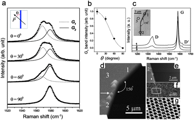
There are two types of achiral edges in graphene nanoribbons—zigzag and armchair edges, defined by the orientation of the hexagons relative to the ribbon length (see Fig. 1). These achiral edges have been observed to dominate over chiral edges after Joule heating.12 Theoretical calculations13 show that zigzag edges are metastable and a planar reconstruction into pentagon-heptagon configurations spontaneously takes place at room temperature. In practice, hydrogenated or oxygenated group passivation during heat treatment14,15 is commonly used to stabilize the edges in air. The detailed chemistry and carrier transport associated with these functionalized edges seem very exciting and further work is necessary along this direction.
 | ||
| Fig. 1 Zigzag and armchair edges in monolayer graphene nanoribbons. The edge structure and the number of atomic rows of carbon atoms normal to the ribbon axis determine the electronic structure and ribbon properties. (Image courtesy of M. Hofmann, MIT). | ||
2. Fabrication
Edged graphene (nanoribbons) can be fabricated in various ways. Quantum mechanical manifestations are most pronounced in narrow, high-quality edged graphene ribbons which have a unique crystallographic orientation. Such graphene nanoribbons (GNRs) are therefore expected to be the most important in graphene electronic device applications. As a result, there has been significant progress in the large-scale production of GNRs in recent years with approaches such as the mechanical exfoliation of graphite, chemical vapor deposition, and lithographic, chemical and sonochemical methods.It is noteworthy that different types of defects are generally present in high or low concentrations on the edges of graphene or graphene nanoribbons.16 From an electronic materials point of view, the presence of hydroxyl groups on the edges could affect the nanoribbon carrier transport, and they should be removed in order to enhance the conductivity of the ribbons. In this context, Tour's group demonstrated that hydrazine is very efficient in removing oxygen from the graphene nanoribbons, thus improving their electrical conductivity.17 However, a great majority of the published work in the graphene field does not emphasize (or study in detail) the importance of edge defects (or edge functionalities), and most of these papers assume that some of the produced graphene nanoribbons are defect-free or very close to that. Therefore, further research involving the detailed chemistry and physics of sharp- and defective-graphene edges should be carried out, with the goal of understanding and eventually reaching control of edge defects.
2.1 Chemical vapor deposition synthesis of GNRs
Although lithographically produced graphene nanoribbons have been commonly used in research laboratories, chemically derived graphene nanoribbons have also been demonstrated.18 Such narrow GNRs however may not be as appealing for bulk industrial level applications due to their multi-step processing and relatively low yields. Therefore, chemical vapor deposition (CVD) offers an alternative approach for preparing large quantities of graphene nanoribbons in a relative short amount of time.19 The first report of CVDgraphite nanoribbon samples is attributed to Murayama and Maeda in 1990.20 Through the decomposition of a reactant gas containing CO/H2/Fe(CO)5 at 400–700 °C, they were able to produce graphite filaments 10 μm long, with a rectangular cross-section 100–700 nm wide and 10–200 nm thick with catalytic Fe3C particles attached to one of the ends (Fig. 2a–c). Using high-resolution TEM they demonstrated that the graphene sheets had a uniform orientation perpendicular to the filament axis and that the graphene edges formed loops at the edges upon thermal annealing at 2800 °C.20 In 2008, two different routes were reported for obtaining graphitic nanoribbons. One of them involved the decomposition of ferrocene and tetrahydrofuran at 950 °C, and the material thus produced contained a mixture of iron filled multiwall carbon nanotubes (MWNTs) and carbon nanoribbons (Fig. 2d and 2e). Although the length and width of the nanoribbons are not discussed in the report, by observation of the published SEM images, the material appears to be ∼200 nm in width and tens of microns in length. The graphitic structure of the carbon nanoribbons was confirmed through X-ray diffraction and TEM measurements, showing that the (002) lattice planes are perpendicular to the axis of growth.21 The second report involved the thermal decomposition at 950 °C of ferrocene/ethanol/thiophene solutions, resulting in the synthesis of a material of ∼40 graphene layers in thickness (stacked parallel to the axis of growth), 20–300 nm in width, and tens of microns in length (Fig. 2f and 2g).19 These ribbons start oxidizing at 700 °C,19 similar to highly oriented pyrolytic graphite (HOPG). This method of CVD synthesis produces large quantities of graphitic nanoribbons, and the as-synthesized nanoribbons have many open edges that are suitable for the study of the structural and electronic properties of graphene edges. | ||
| Fig. 2 CVD grown graphitic nanoribbons. (a) SEM micrographs by Murayama and Maeda of the ribbon-like filaments of graphite prepared at 700 °C, using a bright catalytic particle that is located on the tip of the filament; (b) the ‘tail’ of a ribbon-like filament prepared at 700 °C; (c) the cross-section of a ribbon-like filament prepared at 550 °C ((a), (b) and (c) are reprinted by permission from Macmillan Publishers Ltd: Nature (Ref. 20), copyright (1990)); (d) SEM image of a mixture of carbon nanoribbons and Fe filled MWNTs reported by Mahanandia et al.;21 (e) Magnified SEM image of carbon nanoribbons ((d) and (e) are reprinted from Ref. 21, Copyright (2008), with permission from Elsevier). (f) A low magnification TEM image of many suspended GNRs reported by Campos-Delgado et al.;19 (g) SEM image showing the wavy structure of graphitic nanoribbons ((f) and (g) are reprinted with permission from Ref. 19. Copyright 2008 American Chemical Society). | ||
2.2 Unzipping of CNTs to yield GNRs
Unzipping carbon nanotubes along their longitudinal direction constitutes an alternative method for graphene nanoribbon synthesis. This concept has been adopted by several groups using different reactants and methods. Kosynkin et al.17 reported that MWCNTs can be unzipped by using a chemical treatment with sulfuric acid (H2SO4) and potassium permanganate (KMnO4; an oxidizing agent) as schematized in Fig. 3a. Multi-layer graphene nanoribbons and graphene sheets can be produced in this way. The resulting ribbons are up to 4 μms long, 100–500 nms wide, and 1–30 graphene layer thick. The as-synthesized ribbon edges have many oxygen-containing chemical groups that quench the electrical conductivity of the ribbons, so that reduction or annealing in hydrogen have to be carried out to remove these groups from the edges. More recently, Higginbotham et al.22 reported that the nanotube unzipping process can be optimized by an efficient chemical oxidation process at a somewhat elevated temperature (60 °C) in the presence of a second acid (C2HF3O2 or H3PO4) in addition to the H2SO4/KMnO4 mixture. The presence of the second acid (e.g., H3PO4) inhibits the creation of vacancies in the GNRs due to the protection of the diol groups.22 Interestingly, the degree of oxidation can be adjusted by controlling the amount of oxidizing agent (KMnO4) in the reaction. This process results in much longer (>5 mm) and narrower ribbons (<100 nm), with sharper edges (i.e., more atomically perfect),22 when compared to previous reports in the literature (see Fig. 4). Jiao et al. reported a plasma etching method for unzipping CNTs to form graphene nanoribbons23 (Fig. 3b). In this case, the resulting nanoribbons are 10–20 nms wide, and typically 1–3 graphene layers thick, and show semiconducting properties. Another unzipping method consists of intercalating nanotubes using alkali-metal atoms (e.g.Li, K, Na) and washing out the intercalants. This procedure causes the tube to open along its length. This approach was first reported using Li intercalation in conjunction with ammonia (NH3)24 (Fig. 3b). A previous study has shown that transition metals can cut through graphene sheets under hydrogen flow conditions.25,26 This method can also be used for cutting MWCNTs into GNRs (Fig. 3c) through a method of selective etching. A method for the facile synthesis of high-quality graphene nanoribbons has been reported more recently.27 This method involves two steps in each of the gas phase and liquid phase steps. In the mild gas-phase oxidation step, oxygen reacts with pre-existing defects on the nanotube sidewalls to form etch pits. In the subsequent solution-phase sonication step, sonochemistry and hot gas bubbles enlarge the pits and unzip the tubes. The GNRs thus obtained show smooth edges in the HRTEM image and also show a low (ID/IG) ratio in the Raman D and G band spectra indicating a low defect density. These GNRs show the highest electrical conductance and mobility reported thus far for 10–20 nm wide graphene nanoribbons.27 An alternative method for unzipping carbon nanotubes has been developed by Zettl and co-workers and it consists of passing a high current through a carbon nanotube inside an electron microscope.28 | ||
| Fig. 3 Schematic representation of the method used for unzipping carbon nanotubes to form graphene nanoribbons: (a) chemical route, involving acid reactions that start to break carbon-carbon bonds (e.g., H2SO4 and KMnO4 as oxidizing agents); (b) intercalation-exfoliation of MWNTs, involving treatments in liquid NH3 and Li, and subsequent exfoliation using HCl and heat treatments; (c) catalytic approach, in which metal nanoparticles “cut” the nanotube longitudinally like a pair of scissors, (d) physico-chemical method, by embedding the tubes in a polymer matrix followed by Ar plasma treatment; and (e) the electrical method, by passing an electric current through a nanotube. The resulting structures are either (f) GNRs or (g) graphene sheets. (Images are reprinted with permission from Ref. 16. Copyright 2010 American Chemical Society). | ||
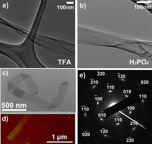 | ||
| Fig. 4 Graphene nanoribbons produced by unzipping carbon nanotubes with an efficient chemical oxidation process. (a,b) Transmission electron microscopy (TEM) images of graphene nanoribbons obtained by unzipping CVD-grown multiwalled carbon nanotubes, using an optimized method involving two acids (TFA or H3PO4) in the presence of KMnO4 and H2SO4 at 65 °C; (c) TEM image of a graphene nanoribbon showing various bends produced using the method by Higginbotham et al.;22 (d) atomic force microscopy (AFM) image of a graphene nanoribbon segment produced by an optimized oxidation method using a second acid (H3PO4) at 65 °C, in addition to KMnO4 and H2SO4. (e) An electron diffraction pattern of a few-layer graphitic nanoribbon obtained using the same conditions as those shown in panel (d). Note the bright spots in (e) correspond to the hexagonal lattice. (Images are reprinted with permission from Ref. 16 and 22. Copyright 2010 American Chemical Society). | ||
Unzipping of nanotubes to yield GNRs appears to be a very promising technique in terms of mass production. This is mainly because several companies around the world, are now able to produce massive quantities of carbon nanotubes per year using the CVD process. However, the atomic control of the edge morphologies of the GNRs still needs to be enhanced and scaled up, in order to take advantage of the special properties of graphene nanoribbons.
2.3 Other methods
In addition to the approaches summarized above, STM lithography has been used to cut graphene nanoribbons from graphene sheets.29Graphene ribbons with a typical width ranging from 2.5 nm to 15 nm, and a length of ∼120 nm were produced in this way, with a measured bandgap of about 0.5 eV for a 2.5 nm-wide armchair GNR using room temperature STS measurements.29 The advantage of using STM lithography is that it is possible to pattern bent junctions with nanometer-precision, as well as to produce a predetermined width and crystallographic orientation of the nanoribbons; such features are hard to achieve presently using other cutting techniques. This advantage stems from the possibility of achieving excellent atomic resolution using STM on flat graphitic surfaces. However, STM lithography suffers from low throughput and equipment accessibility, two issues that make it unlikely for this technique to be used in large-scale applications. Another chemical method for atomically precise bottom-up fabrication of GNRs has recently been developed by Cai et al.,30 which involves a precursor monomer on a gold substrate that forms GNRs through dehalogenation and cyclodehydrogenation steps. This method produces GNRs with well controlled widths and various shapes. However, challenges remain in fabricating these GNRs on a technology relevant substrate, or in transferring the GNRs onto an arbitrary substrate.3. Characterization
Graphene edges are investigated using a variety of characterization techniques. Advanced transmission electron microscopes (TEM) are commonly used in evaluating graphene edge structures, and Raman spectroscopy is advantageous for distinguishing zigzag from armchair edges and for studying the chirality-dependent edge disorder and the quantum confinement of the electrons in 1D band structures. The use of scanning tunneling microscopy (STM) and spectroscopy (STS) for studying the electronic states at graphene edges is also a promising research field, and STS/STM can be used to study the magnetic properties of graphene edges, which is reviewed in detail in Ref. 31.3.1 TEM characterization and in situ Joule heating
High resolution transmission electron microscopy (HRTEM) is a highly sensitive tool for studying graphene edges. Graphene edges in each layer typically exhibit a dark line in the TEM image (see Fig. 5b), which enables counting the number of layers in as-synthesized graphene samples.32,33 The edge roughness can also be directly estimated using HRTEM imaging.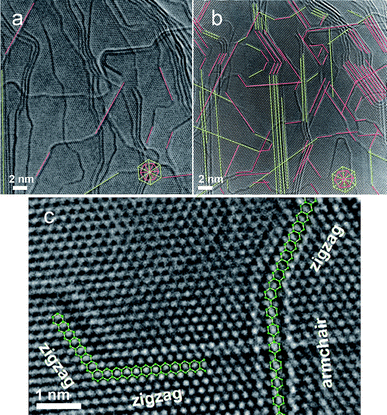 | ||
| Fig. 5 TEM images showing sharp zigzag and armchair edges formed from irregular edges using an in situ Joule heating method.12 (a) TEM image shows irregular edges in graphitic nanoribbons before Joule heating. (b) Sharp zigzag (pink lines) and armchair (green lines) edges are formed after Joule heating. (c) High resolution TEM image shows well-defined zigzag and armchair edges (as illustrated by green hexagons) after Joule heating. (Images are from Ref. 12. Reprinted with permission from AAAS). | ||
Significant progress has been reported in the TEM characterization of graphene edges.12,34–41 For example, in a previous study developed by some of the present authors,31 CVD-grown graphitic nanoribbon edges have been characterized using a conventional HRTEM (2010F) instrument integrated with an STM holder. Using this setup, edge modification by in situ Joule heating was demonstrated for the first time.12 In this experiment, a piece of graphitic nanoribbon material (Fig. 2f) is suspended in between two electrodes inside the TEM, and a voltage is applied across the ribbon length. After a significant amount of time (typically 20 min) in the HRTEM and exposure to electron beam irradiation, the graphitic nanoribbon becomes highly defective. Under these conditions the edges of each graphene layer show irregular structures (Fig. 5a). As the voltage is increased across the ribbon, the material gets significant resistive Joule heating, resulting in in-situ crystallization and edge reconstruction. The resulting material shows almost entirely achiral edges (either zigzag or armchair edges (Fig. 5b)). Atomically smooth zigzag, armchair edges, and edge junctions can be readily resolved here (Fig. 5c). This postprocessing approach shows that Joule heating in an electron microscope provides a possible way of modifying rough edges in graphene nanoribbons, and provides a further step towards the use of graphene nanoribbons for electronic device applications. Various consistent explanations based on first principles calculations have been provided both to explain the details of the Joule heating mechanism in cleaning the edges,12,42,43 and to highlight the role of electron irradiation induced by the TEM itself in the process.43
Zettl and co-workers40 have also been able to directly observe 5–7 and Thrower-Stone-Wales (TSW)44,45 bulk defects as well as 5–7 edge defects on isolated graphene surfaces using aberration corrected transmission electron microscopy (see Fig. 6 and Fig. 7).
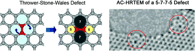 | ||
| Fig. 6 (Left) Molecular model showing the transformation of 4 adjacent hexagons into a 5-7-7-5 defect or a Thrower-Stone-Wales defect, and (right) HRTEM image showing two 5-7-7-5 defects located on the edges (red circles) of a hole in a graphene surface. (Images are taken from movies from supplementary material of Ref. 40. Reprinted with permission from AAAS). | ||
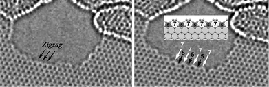 | ||
| Fig. 7 HRTEM images showing a zigzag edge near a hole region of a graphene layer (left) transformed into a 5–7 defect edge (right). (Images are adapted from movies in the supplementary material of Ref. 40. Reprinted with permission from AAAS). | ||
In order to resolve the atomic structures at graphene edges, advanced TEM techniques are required. Using an aberration-corrected TEM instrument combined with a monochromator (TEAM 0.5), which has sub Angstrom resolution, the stability of mechanically exfoliated graphene edges under electron beam irradiation has been studied in real time. Under these conditions, edge reconstruction is observed (see Fig. 6). The abundance of zigzag edges lends evidence for a more stable zigzag configuration under these conditions.40 In Ref. 38 open and closed (folded) edges in exfoliated HOPG materials have been studied under conditions when such edges are stable. After furnace annealing at ∼2000 °C, open edges are found to become less stable so that most of the open edges join with edges in the neighboring layer to form well-stacked loops. Finally, note that Ref. 39 reports on the in situ observation of graphene sublimation and multi-layer edge reconstructions at elevated temperatures.
3.2 Raman spectroscopy
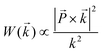
Compared to the TEM characterization of graphene edges, Raman spectroscopy provides a complementary, yet quite different characterization tool that is also suitable for distinguishing between zigzag and armchair edges in graphene nanoribbons and studying edge disorder. It has been found that the Raman peak of nanographite ribbons (on a HOPG substrate) exhibits an intensity dependence on the light polarization direction relative to the nanographite ribbon axis,46 as shown in Fig. 8a. The Raman spectrum here is composed of two peaks centered at 1568 cm−1 (G1 peak) and 1579 cm−1 (G2 peak). The G2 peak frequency, which remains unchanged when varying the polarization angle (θ) of the incident beam with respect to the ribbon axis direction, comes from the HOPG substrate. In contrast, the G1 feature in Fig. 8a comes from the nanographite ribbon, and its intensity varies with the polarization of the incident light. The intensity decreases with increasing θ and can be fitted to a cos2θ curve (Fig. 8b). This curve originates from the relationship between the probability of light absorption W(![[k with combining right harpoon above (vector)]](https://www.rsc.org/images/entities/i_char_006b_20d1.gif) ) and the wave vector of the electron k written as
) and the wave vector of the electron k written aswhere
![[P with combining right harpoon above (vector)]](https://www.rsc.org/images/entities/i_char_0050_20d1.gif) is the polarization vector of the incident light. Since van Hove singularities occur in the
is the polarization vector of the incident light. Since van Hove singularities occur in the ![[T with combining right harpoon above (vector)]](https://www.rsc.org/images/entities/i_char_0054_20d1.gif) direction (θ = 0) in real space due to the 1D quantum confinement structure in the electronic density of states, a large Raman signal is obtained when the light is in resonance with the excitonic optical transition energies between van Hove singularities. The Raman G-band intensities are, therefore, different for interior regions of a nanographite ribbon and at the edges. The G-band intensity of a GNR is also dependent on the GNR width and crystalline direction. Thus it is only the electronic vector along the
direction (θ = 0) in real space due to the 1D quantum confinement structure in the electronic density of states, a large Raman signal is obtained when the light is in resonance with the excitonic optical transition energies between van Hove singularities. The Raman G-band intensities are, therefore, different for interior regions of a nanographite ribbon and at the edges. The G-band intensity of a GNR is also dependent on the GNR width and crystalline direction. Thus it is only the electronic vector along the ![[K with combining right harpoon above (vector)]](https://www.rsc.org/images/entities/i_char_004b_20d1.gif) T direction in reciprocal space that is involved in the optical absorption process. When θ = 0, then we have //T, and G1 reaches its maximum value; however, when θ reaches 90°, the G1 peak should vanish and a cos2θ dependence of the intensity is obtained, as shown in Fig. 8b. This polarization dependent behavior allows the Raman technique to distinguish between armchair and zigzag edges.
T direction in reciprocal space that is involved in the optical absorption process. When θ = 0, then we have //T, and G1 reaches its maximum value; however, when θ reaches 90°, the G1 peak should vanish and a cos2θ dependence of the intensity is obtained, as shown in Fig. 8b. This polarization dependent behavior allows the Raman technique to distinguish between armchair and zigzag edges.
 | ||
| Fig. 8 Raman spectrum on GNR edges.46,47 (a) Raman spectra obtained for light incident with different polarization angles (θ) with respect to the ribbon axis direction in nanographite ribbon sheets. The inset shows a schematic figure of the sample (vertical gray line) denoting the direction between the ribbon axis and the light polarization vector. (b) Intensity of the G1 Raman peak versus θ. The dotted line is a cos2θ theoretical fit to the experimental points. (Images (a) and (b) are adapted from Ref. 46). (c) Raman spectra obtained in three different regions of an HOPG sample (see (d)). The inset shows an optical image of an edge region of a sample and the regions where spectra 1, 2 and 3 were taken (open circles). (d-e) AFM images of the step on the HOPG substrate where the Raman spectra shown in (c) were taken. (f) The STM measurements and (g) The FFT (fast Fourier transform) filtered image verifying the zigzag edge configuration in the marked region 2 in (c, d). (Images (c)-(g) are reprinted with permission from Ref. 47. Copyright 2004 by the American Physical Society). | ||
For example, Figs. 8d–g show the influence of the edge structure on the Raman spectra of edges in HOPG.47 The edge configurations shown here are determined by STM measurements. It is found that the disorder-induced D band in the Raman spectra also provides a powerful way to distinguish armchair from zigzag edges. Here we see that the D band intensity is about 3 times less intense for a zigzag edge (spectrum 2) compared to that for an armchair edge (spectrum 1), when normalized to their G band intensities. The residual intensity of the D band from the zigzag edge is attributed to disorder in this edge structure. This shows that the observation of the D-band could be useful for characterizing the defect structure in nanographite-based devices. Recent calculations of the Raman spectra of graphene ribbons including the effect of the matrix elements of the Raman tensor48 represent a first step in a quantitative approach to using the Raman G-band scattering intensities to distinguish between armchair and zigzag edges.
3.3 Defective edges
The most common defects one finds in graphene nanoribbons are: vacancies, heptagon-pentagon pairs (STW transformations), loops and interstitials. While heptagon-pentagon pairs and loops preserve the connectivity of the nanoribbon, interstitials and vacancies do not. Therefore, scientists must now work on defect edge engineering in order to tailor the reactivity and transport properties of graphene edges. For example, it could be possible to achieve specificity for sensing different types of molecules or to anchor specific polymer groups at the edges of GNRs, in order to produce stable and well dispersed composites or suspensions. In addition, electronic and thermal transport properties are important for understanding the effect of specific and controlled defects on graphene edges. It is clear that edge chemistry and the physics of GNRs, a field which is just emerging, could lead to unexpected catalytic reactions, novel field effect transistors, efficient electrodes for Li-ion batteries, anchoring centers for assembling heavy metal, highly conducting and transparent films, drug delivery devices, and other applications.Further studies considering edges having pentagon-heptagon (5-7) or pentagon-octagon-pentagon (5-8-5) rows (as schematized in Fig. 9) need to be carried out in detail from both experimental and theoretical points of view. For example, very recently, Batzill and coworkers identified the presence of a 5-8-5 defect line within a graphene sheet using STM.49 These lines behave as quantum wires. This finding indicates that other defect topologies should also be considered and studied. In addition, Botello-Méndez et al. also demonstrated that hybrid ribbons interconnecting zigzag and armchair nanoribbons behave as spin polarized conductors.50 Finally, it is also possible to have non-carbon atoms within either ribbons or graphene using heteroatomic doping atoms, such as B and N.51–56 These systems need to be studied further along with the presence of defects on the edges caused by the introduction of non-hexagonal rings.13
 | ||
| Fig. 9 Schematics of graphene nanoribbons with a perfect zigzag edge, and edges with 5-7 defects and 5-8-5 defects, respectively. (Image courtesy of L. P. Wang, MIT). | ||
3.4 Folded edges
As previously mentioned, folded edges are often observed in TEM characterizations of multi-layer graphene. Folded edges are formed when the edges of adjacent graphene layers are connected with each other to form a curved closed loop. Folded edges (see Fig. 10) have quite a different structure from other carbon nanostructures, and therefore should have a different chemistry and reactivity as compared to the open edges. Thus they should have different applications. For this reason, it is important to understand the conditions under which folded edges form, and how to prevent edge folding (or loop formation at multi-layer graphene edges) when folded edges are undesirable. | ||
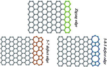
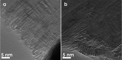
| Fig. 10 Folded edges formed across graphene layers by furnace heat treatment. (a) The pristine sample before heat treatment shows open edges. (b) At 1500 °C, single loops (folded edges) are formed between adjacent graphene layers. (c) At 2800 °C, multiple loops (folded edges) are formed. (d) A schematic shows the single, double and multiple loop (folded edge) configurations in graphitic nanoribbons. (Images are reprinted with permission from Ref. 57. Copyright 2009, American Vacuum Society). | ||
Ref. 57 describes two methods by which CVD-grown pristine open edged graphitic nanoribbons (see Fig. 10a) can develop into stable closed loops. One method consists of furnace heat treatment to temperature in excess of 1500 °C. In this case, the shape and size of the loops can be tuned by varying the annealing temperature. Fig. 10a shows the open edges in a pristine sample before heat treatment. The open edges of this sample are passivated by heat treatment, and single loops are formed between adjacent layers at 1500 °C in order to minimize the free energy (Fig. 10b). Some double loops are formed by heat treatment to 1500 °C and multi-loops are formed when using higher heat treatment temperatures. For example, faceted multiple loops are formed at 2800 °C, as can be readily resolved in TEM images (Fig. 10c). Fig. 10d shows the schematics of different loop formations at the edge of multi-layer graphene. A similar observation was made by the Iijima group in Ref. 38, where an HOPG sample is heat treated in a furnace for several hours at 2000 °C. In this case, TEM micrographs of the heat treated sample clearly show loop formation at the edges. Another method for loop formation, other than furnace heat treatment, is by direct resistive Joule heating across pristine graphitic nanoribbons inside a TEM, as mentioned in section 3.1 above. It is found that resistive Joule heating without prior electron beam irradiation damage induces effective loop formation in a way very similar to that of furnace heat treated samples (see Fig. 11).
 | ||
| Fig. 11 TEM images of folded edges that are formed across graphene layers by resistive Joule heating (a) near the electrode, and (b) further away from the electrode. (Images are reprinted with permission from Ref. 57. Copyright 2009, American Vacuum Society). | ||
The key difference between open edges and loop formation is the significant role played by electron beam irradiation when applied before in situ Joule heating. Irradiation indeed enables edge modification and sharp open edge formation in CVD-grown graphitic nanoribbons. Recent theoretical work by Cruz-Silva et al.43 provided an atomistic analysis to highlight the reasons why loops are formed by Joule heating alone, while adjacent layers do not coalesce when Joule heating is applied after high energy electron irradiation. This theoretical work based on large-scale quantum molecular dynamics calculations indicates that the presence of both vacancies and interstitials (so-called “Frenkel pairs”) are essential for keeping graphene layers parallel to one another and for preventing adjacent edges from coalescing (loop formation). Electron beam irradiation, based on previous reports,35,58,59 is likely to provide the driving force for inducing vacancies and interstitials in graphitic nanoribbons. On one hand, the introduction of vacancies increases the surface reactivity and interlayer interaction far away from the edges. On the other hand, the interstitials provide effective feedstock to ensure interlayer cross-link creation which keeps the layers parallel and prevents loop formation (see Fig. 12). Quantum transport calculations further confirm that interlayer cross-linking increases the backscattering of electrons and promotes interlayer transport.43 Therefore the cross-linking sites are key for both Joule heating and defect annealing, and such sites are susceptible to being healed during the Joule heating process.
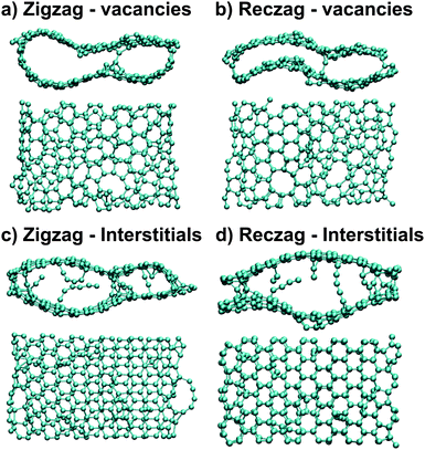 | ||
| Fig. 12 Molecular models showing the final configurations for graphene nanoribbons with vacancy (a),(c) and interstitial defects (b),(d). Zigzag ribbons create loops with both vacancies (a) and interstitials (c), while the reconstructed zigzag (reczag) edges do not show this behavior and rather show increased structural order. Interstitials lead to the formation of monoatomic carbon chains in both zigzag and reczag edges, due to the low reactivity of a graphene surface. (Images are reprinted from Ref. 43 with permission). | ||
Very recently, Joly, et al.60 investigated the edge states in graphene nanoribbons prepared by the CVD method, using near-edge X-ray absorption fine structure (NEXAFS) and electron spin resonance (ESR) spectroscopy. It was noted that the C 1s to π* transitions of nanoribbon samples, correspond to the C 1s to edge-state transitions of nanographenes. As the CVD ribbons were annealed at high temperatures in an Ar atmosphere, the contribution of the edge states decreased due to the loop formation. These results confirm the presence of magnetic edge states in the edges of graphene nanoribbons and provide significant insight into these magnetic edge states (see Fig. 13).
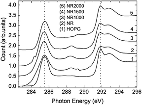 | ||
| Fig. 13 Carbon K-edge NEXAFS spectra of the pristine graphene NR, NR1000, NR1500, and NR2000. The pristine sample (NR) and HOPG are also given for comparison. The count value for HOPG given in the figure is reduced to half of the original count to make the count scale comparable with the other traces. The C 1s to π* (285.5 eV) and σ* (291.85 eV) transitions are indicated by dotted vertical lines. (Image is reprinted from Ref. 60 with permission). | ||
Conclusions and outlook
Since 2004, the research on graphene edges has attracted increasing attention and has undergone rapid progress. Zigzag edges can be distinguished from armchair edges because of their high electron density of states near the Fermi level9,62 relative to armchair edges. The fabrication of graphene edges and graphene nanoribbons has made significant advances within the last two years towards the large scale production of smooth edges and narrow ribbons. With the stringent demands of electronic device applications and the desire to continually promote fundamental physics studies, more efforts in improving the synthesis conditions as well as the post-growth treatment procedures of graphene edges are foreseeable. In the meanwhile, the characterization of graphene edges has also progressed significantly and is now pushing the limit of nanomaterials characterization techniques. Integrated characterization techniques, such as combined STM with TEM, combined Raman spectroscopy with other electron microscopy techniques, are likely to take place, which will facilitate our understanding of advanced nanomaterials and their development towards applications. In addition, study of the magnetoresistance of graphene nanoribbon-based FETs is another emerging research field that is likely to gain more momentum towards various applications.61Although extensively investigated in the laboratory, the fabrication of graphene edges in electronic device applications is still facing many challenges, including the creation of both smooth edges and controlled narrow graphene ribbons that can open a sizable and well-defined bandgap and there are still many open issues and opportunities for further research effort. Given the short history of this field, the progress has been impressive and significant developments in graphene edge applications are expected to occur in the near future.
Acknowledgements
The authors gratefully acknowledge support from NIRT/NSF/CTS-05-06830 (XJ) and Navy-ONR-MURI-N00014-09-1-1063 (MSD). We thank JST-Japan for Research funding the Center for Exotic NanoCarbon Project, the Japanese regional Innovation Strategy Program by the Excellence (MT). We also thank FAPERJ for research funding in Brazil (JCD).Notes and references
- H. P. Boehm, A. Clauss, G. Fischer and U. Hofmann, Proceedings of the Fifth Conference on Carbon, Pergamon Press, 1962 Search PubMed.
- K. S. Novoselov, A. K. Geim, S. V. Morozov, D. Jiang, Y. Zhang, S. V. Dubonos, I. V. Grigorieva and A. A. Firsov, Science, 2004, 306, 666–669 CrossRef CAS.
- K. S. Novoselov, A. K. Geim, S. V. Morozov, D. Jiang, M. I. Katsnelson, I. V. Grigorieva, S. V. Dubonos and A. A. Firsov, Nature, 2005, 438, 197–200 CrossRef.
- Y. B. Zhang, Y. W. Tan, H. L. Stormer and P. Kim, Nature, 2005, 438, 201–204 CrossRef CAS.
- A. K. Geim and K. S. Novoselov, Nat. Mater., 2007, 6, 183–191 CrossRef CAS.
- K. S. Novoselov, Z. Jiang, Y. Zhang, S. V. Morozov, H. L. Stormer, U. Zeitler, J. C. Maan, G. S. Boebinger, P. Kim and A. K. Geim, Science, 2007, 315, 1379–1379 CrossRef CAS.
- C. Lee, X. D. Wei, J. W. Kysar and J. Hone, Science, 2008, 321, 385–388 CrossRef CAS.
- G. G. Naumis, M. Terrones, H. Terrones and L. M. Gaggero-Sager, Appl. Phys. Lett., 2009, 95.
- Y. W. Son, M. L. Cohen and S. G. Louie, Nature, 2006, 444, 347–349 CrossRef CAS.
- M. Y. Han, B. Ozyilmaz, Y. B. Zhang and P. Kim, Phys. Rev. Lett., 2007, 98, 4 Search PubMed.
- F. Schwierz, Nat. Nanotechnol., 2010, 5, 487–496 CrossRef CAS.
- X. T. Jia, M. Hofmann, V. Meunier, B. G. Sumpter, J. Campos-Delgado, J. M. Romo-Herrera, H. B. Son, Y. P. Hsieh, A. Reina, J. Kong, M. Terrones and M. S. Dresselhaus, Science, 2009, 323, 1701–1705 CrossRef CAS.
- P. Koskinen, S. Malola and H. Hakkinen, Phys. Rev. Lett., 2008, 101, 115502 CrossRef.
- Y. Kobayashi, K. Fukui, T. Enoki, K. Kusakabe and Y. Kaburagi, Phys. Rev. B: Condens. Matter Mater. Phys., 2005, 71, 193406 CrossRef.
- T. Fukunaga, K. Itoh, S. Orimo, M. Aoki and H. Fujii, J. Alloys Compd., 2001, 327, 224 CrossRef CAS.
- M. Terrones, ACS Nano, 2010, 4, 1775–1781 CrossRef CAS.
- D. V. Kosynkin, A. L. Higginbotham, A. Sinitskii, J. R. Lomeda, A. Dimiev, B. K. Price and J. M. Tour, Nature, 2009, 458, 872–U875 CrossRef CAS.
- X. L. Li, X. R. Wang, L. Zhang, S. W. Lee and H. J. Dai, Science, 2008, 319, 1229–1232 CrossRef CAS.
- J. Campos-Delgado, J. M. Romo-Herrera, X. T. Jia, D. A. Cullen, H. Muramatsu, Y. A. Kim, T. Hayashi, Z. F. Ren, D. J. Smith, Y. Okuno, T. Ohba, H. Kanoh, K. Kaneko, M. Endo, H. Terrones, M. S. Dresselhaus and M. Terrones, Nano Lett., 2008, 8, 2773–2778 CrossRef CAS.
- H. Murayama and T. Maeda, Nature, 1990, 345, 791–793 CrossRef CAS.
- P. Mahanandia, K. K. Nanda, V. Prasad and S. V. Subramanyam, Mater. Res. Bull., 2008, 43, 3252–3262 Search PubMed.
- A. L. Higginbotham, D. V. Kosynkin, A. Sinitskii, Z. Z. Sun and J. M. Tour, ACS Nano, 2010, 4, 2059–2069 CrossRef CAS.
- L. Y. Jiao, L. Zhang, X. R. Wang, G. Diankov and H. J. Dai, Nature, 2009, 458, 877–880 CrossRef CAS.
- A. G. Cano-Marquez, F. J. Rodriguez-Macias, J. Campos-Delgado, C. G. Espinosa-Gonzalez, F. Tristan-Lopez, D. Ramirez-Gonzalez, D. A. Cullen, D. J. Smith, M. Terrones and Y. I. Vega-Cantu, Nano Lett., 2009, 9, 1527–1533 CrossRef CAS.
- L. Ci, Z. P. Xu, L. L. Wang, W. Gao, F. Ding, K. F. Kelly, B. I. Yakobson and P. M. Ajayan, Nano Res., 2008, 1, 116–122 CrossRef CAS.
- L. C. Campos, V. R. Manfrinato, J. D. Sanchez-Yamagishi, J. Kong and P. Jarillo-Herrero, Nano Lett., 2009, 9, 2600–2604 CrossRef CAS.
- L. Y. Jiao, X. R. Wang, G. Diankov, H. L. Wang and H. J. Dai, Nat. Nanotechnol., 2010, 5, 321–325 CrossRef CAS.
- K. Kim, A. Sussman and A. Zettl, ACS Nano, 2010, 4, 1362–1366 CrossRef CAS.
- L. Tapaszto, G. Dobrik, P. Lambin and L. P. Biro, Nat. Nanotechnol., 2008, 3, 397–401 CrossRef CAS.
- J. M. Cai, P. Ruffieux, R. Jaafar, M. Bieri, T. Braun, S. Blankenburg, M. Muoth, A. P. Seitsonen, M. Saleh, X. L. Feng, K. Mullen and R. Fasel, Nature, 2010, 466, 470–473 CrossRef CAS.
- T. Enoki, Y. Kobayashi and K. I. Fukui, Int. Rev. Phys. Chem., 2007, 26, 609–645 CrossRef CAS.
- J. C. Meyer, A. K. Geim, M. I. Katsnelson, K. S. Novoselov, T. J. Booth and S. Roth, Nature, 2007, 446, 60–63 CrossRef CAS.
- K. S. Novoselov, D. Jiang, F. Schedin, T. J. Booth, V. V. Khotkevich, S. V. Morozov and A. K. Geim, Proc. Natl. Acad. Sci. U. S. A., 2005, 102, 10451–10453 CrossRef CAS.
- J. C. Meyer, C. O. Girit, M. F. Crommie and A. Zettl, Nature, 2008, 454, 319–322 CrossRef CAS.
- J. H. Warner, M. H. Rummeli, L. Ge, T. Gemming, B. Montanari, N. M. Harrison, B. Buchner and G. A. D. Briggs, Nat. Nanotechnol., 2009, 4, 500–504 CrossRef CAS.
- J. H. Warner, M. H. Rummeli, T. Gemming, B. Buchner and G. A. D. Briggs, Nano Lett., 2009, 9, 102–106 CrossRef CAS.
- J. H. Warner, F. Schaffel, M. H. Rummeli and B. Buchner, Chem. Mater., 2009, 21, 2418–2421 Search PubMed.
- Z. Liu, K. Suenaga, P. J. F. Harris and S. Iijima, Phys. Rev. Lett., 2009, 102, 015501 CrossRef.
- J. Y. Huang, F. Ding, B. I. Yakobson, P. Lu, L. Qi and J. Li, Proc. Natl. Acad. Sci. U. S. A., 2009, 106, 10103–10108 Search PubMed.
- C. O. Girit, J. C. Meyer, R. Erni, M. D. Rossell, C. Kisielowski, L. Yang, C. H. Park, M. F. Crommie, M. L. Cohen, S. G. Louie and A. Zettl, Science, 2009, 323, 1705–1708 CrossRef CAS.
- J. H. Warner, M. H. Rummeli, A. Bachmatiuk and B. Buchner, Nanotechnology, 2010, 21, 325702 Search PubMed.
- M. Engelund, J. A. Furst, A. P. Jauho and M. Brandbyge, Phys. Rev. Lett., 2010, 104, 036807 Search PubMed.
- E. Cruz-Silva, A. R. Botello-Mendez, Z. Barnett, X. Jia, M. S. Dresselhaus, H. Terrones, M. Terrones, B. G. Sumpter and V. Meunier, Phys. Rev. Lett., 2010, 105, 045501 Search PubMed.
- A. J. Stone and D. J. Wales, Chem. Phys. Lett., 1986, 128, 501–503 CrossRef CAS.
- P. A. Thrower, Chemistry and Physics of Carbon, 1969, 5, 261–262 Search PubMed.
- L. G. Cancado, M. A. Pimenta, B. R. A. Neves, G. Medeiros-Ribeiro, T. Enoki, Y. Kobayashi, K. Takai, K. Fukui, M. S. Dresselhaus, R. Saito and A. Jorio, Phys. Rev. Lett., 2004, 93, 047403 CrossRef CAS.
- L. G. Cancado, M. A. Pimenta, B. R. A. Neves, M. S. S. Dantas and A. Jorio, Phys. Rev. Lett., 2004, 93, 247401 CrossRef CAS.
- R. Saito, M. Furukawa, G. Dresselhaus and M. S. Dresselhaus, J. Phys.: Condens. Matter, 2010, 22, 334203 Search PubMed.
- J. Lahiri, Y. Lin, P. Bozkurt, I. I. Oleynik and M. Batzill, Nat. Nanotechnol., 2010, 5, 326–329 CrossRef CAS.
- A. R. Botello-Mendez, E. Cruz-Silva, F. Lopez-Urias, B. G. Sumpter, V. Meunier, M. Terrones and H. Terrones, ACS Nano, 2009, 3, 3606–3612 CrossRef CAS.
- L. Ci, L. Song, C. H. Jin, D. Jariwala, D. X. Wu, Y. J. Li, A. Srivastava, Z. F. Wang, K. Storr, L. Balicas, F. Liu and P. M. Ajayan, Nat. Mater., 2010, 9, 430–435 CrossRef CAS.
- T. Tada and K. Yoshizawa, J. Phys. Chem. B, 2003, 107, 8789–8793 Search PubMed.
- P. A. Denis, Chem. Phys. Lett., 2010, 492, 251–257 CrossRef CAS.
- L. R. Radovic and B. Bockrath, J. Am. Chem. Soc., 2005, 127, 5917–5927 CrossRef CAS.
- F. Cervantes-Sodi, G. Csanyi, S. Piscanec and A. C. Ferrari, Phys. Rev. B: Condens. Matter Mater. Phys., 2008, 77, 165427 CrossRef.
- X. R. Wang, X. L. Li, L. Zhang, Y. Yoon, P. K. Weber, H. L. Wang, J. Guo and H. J. Dai, Science, 2009, 324, 768–771 CrossRef CAS.
- X. T. Jia, J. Campos-Delgado, E. E. Gracia-Espino, M. Hofmann, H. Muramatsu, Y. A. Kim, T. Hayashi, M. Endo, J. Kong, M. Terrones and M. S. Dresselhaus, J. Vac. Sci. Technol., B, 2009, 27, 1996–2002 Search PubMed.
- A. V. Krasheninnikov and F. Banhart, Nat. Mater., 2007, 6, 723–733 CrossRef CAS.
- J. A. Rodriguez-Manzo and F. Banhart, Nano Lett., 2009, 9, 2285–2289 CrossRef CAS.
- V. L. J. Joly, M. Kiguchi, S. J. Hao, K. Takai, T. Enoki, R. Sumii, K. Amemiya, H. Muramatsu, T. Hayashi, Y. A. Kim, M. Endo, J. Campos-Delgado, F. Lopez-Urias, A. Botello-Mendez, H. Terrones, M. Terrones and M. S. Dresselhaus, Phys. Rev. B: Condens. Matter Mater. Phys., 2010, 81, 245428 CrossRef.
- J. Bai, R. Cheng, F. Xiu, L. Liao, M. Wang, A. Shailos, K. L. Wang, Y. Huang and X. Duan, Nat. Nanotechnol., 2010 Search PubMed.
- K. Nakada, M. Fujita, G. Dresselhaus and M. S. Dresselhaus, Phys. Rev. B: Condens. Matter, 1996, 54, 17954 CrossRef CAS.
| This journal is © The Royal Society of Chemistry 2011 |