Arranging junctions for nanofibers†
Mengmeng
Li
ab,
Dayong
Yang
*a,
Yunze
Long
b and
Hongwei
Ma
*a
aSuzhou Institute of Nano-Tech and Nano-Bionics, Chinese Academy of Sciences, Suzhou 215125, China. E-mail: dyyang2008@sinano.ac.cn; hwma2008@sinano.ac.cn
bCollege of Physics science, Qingdao University, Qingdao 266071, China
First published on 25th November 2009
Abstract
Epoxy in electrospun nanofibers acting as adhesive generates junctions between nanofibers and thus forms stable three-dimensional networks.
One-dimensional nanomaterials such as wires and fibers are attractive owing to their unique properties and applications.1,2 Some applications such as substrates for immunoassays 3 and supports for catalysts4 make use of the assembly of these building blocks. Therefore, how to assemble the building blocks into stable entities is critical for applications. This communication provides a general strategy to arrange junctions among nanofibers that lead to the formation of a stable three-dimensional (3D) nanofiber network.
Among the solutions for fabricating one-dimensional nanomaterials, electrospinning (ES) possesses several attractive features: comparatively low cost, relatively high production rate, the ability to generate materials with large specific surface areas, and applicability to many types of materials, making ES mats suitable for many applications.3–11 Studies about ES mainly focused on the morphology control of individual fibers. Relatively few studies are concerned with the process of fiber assembly, which determines the properties of the resulting membrane as well as its applications. In conventional ES, nanofibers are simply deposited on the collector without any further treatments, resulting in a nonwoven membrane in which nanofibers are randomly oriented.8 Consequently, there are insufficient interactions between nanofibers. We believe that the nonwoven nature and lack of interactions between fibers account for the instability of ES mats,3 such as deformation, delamination or crinkling at the macro-level and sliding of fibers at the micro-level. This instability greatly jeopardizes the performance of various applications of ES mats.
In the conventional textile industry, fibers are woven into interleaving orderly fabric arrays, where physical contact and entanglements act as junctions. In the construction industry, reinforcing steel bars are adhered together to form stable scaffold, where solder act as a junction. But when miniaturizing the size of fibers down to the micro- or nanoscale, it is difficult to manipulate single fibers and further arrange fibers into stable structures. The diameter of electrospun fibers ranges from several micrometres to a few nanometres. Furthermore, the ES rate is very high and uncontrollable, which makes it impossible to manipulate single fibers during the ES process.12 Thus, it will be extremely difficult to interleave nanofibers from ES to woven textile, like in the textile industry. Alternatively, one could try the solder strategy widely used in the construction industry: generating soldered junctions among nanofibers. Previously, solvent-vapor-mediated welding13 and heat welding14 were developed to produce junctions at the intersections of nanofibers by softening the hard nanofibers. Because these two methods required precise control of the vapor pressure and temperature, other more practicable methods are desired.
We report herein a simple method for arranging junctions between nanofibers that uses epoxy as an additive in the ES solution. The resulting nanofibers have epoxy at their surfaces and overlay each other to form many contact points, where epoxy acts as an adhesive after a regular curing procedure to covalently link electrospun nanofibers together to form stable 3D networks. This strategy contains three steps. First, we mixed epoxy prepolymer and the corresponding curing agent with polymer solutions. Second, we electrospun the mixed solution into nanofibers. Third, we heated nanofibers at elevated temperature to cure the epoxy resin. We further developed two new methods to confirm the formation of junctions and qualitatively evaluate the mechanical performance of junctions.
We conducted the experiments on a conventional ES setup. As shown in Scheme 1a), a Taylor cone formed under high voltage and ES mats ejected from the cone rushed to the collector. Because the ES process is very fast (estimated to be 5 m s−1) and the micro- or nano-scale of the ES mats results in large specific areas, the solvents evaporate very quickly so that the ESnanofibers are mostly in the “dry” state. The dry nanofibers physically contact each other, but there are no strong interactions between them [Scheme 1b)]. Moreover, the ES mats deposit in a layer-by-layer fashion, so the entanglement forces between nanofibers are very weak. As a result the ES mats as an integrative membrane are fragile, and deformation, delamination or crinkling often happen. We believed that if we could arrange junctions at the cross of every two fibers, the nanofibers will assemble into 3D networks and the membrane will be stable. For this purpose, we first introduced epoxy resin together with the corresponding curing agent into the polymer solution, then electrospun the blends and finally heated the ES mats so as to cure the epoxy resin. As a result, junctions formed at the crossing-point of every pair of nanofibers [Scheme 1c)].
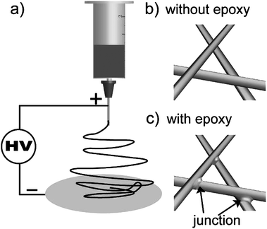 | ||
| Scheme 1 a) Illustration of the electrospinning set-up. b) No junctions exist between fibers that are electrospun without epoxy resin. c) Junctions exist between fibers that are electrospun with epoxy resin as an adhesive. | ||
We propose the following mechanism for the formation of the junctions: Epoxy resin is a thermosetting material, which is composed of two separate components, i.e., prepolymer and curing agent. The prepolymer is a viscous liquid; but after mixing with a curing agent and being heated at elevated temperature, the blend changes from a liquid to a solid. During ES, the blends are electrospun into nanofibers. At this time, the solvents evaporate and the epoxy prepolymer does not cure and is sticky. Therefore, when the nanofibers contact each other, they will stick together due to the viscous epoxy prepolymer, but not covalently bind. After heating the nanofibers, curing agent causes epoxy prepolymer to form cross-links via covalent bonds. Thus, the epoxy resin at the intersection of each pair of nanofibers forms a junctions that links the nanofibers together.
The determining factor for the formation of junctions is the adding amount of epoxy. The polymer used was poly(methyl methacrylate) (PMMA), and the solvent was a mixture of dimethylformamide (DMF) and tetrahydrofuran (THF) (1![[thin space (1/6-em)]](https://www.rsc.org/images/entities/char_2009.gif) :1 by weight). We first determined the optimal ES parameters for pure PMMA as following: PMMA concentration 10 wt%, voltage 25 kV, work distance 15 cm, and ES time 5 min. With these parameters, we prepared smooth and continuous PMMAnanofibers with uniform diameter. In Fig. 1a), we observe that the image of the surface is clear but the image of the underlayer is diffuse, because the SEM electrons focus on the top surface. This observation was attributed to the loose property of PMMA ES mats. The enlarged SEM image [Fig. 1g)] clearly shows that there are no junctions between nanofibers. We added different amounts of epoxy into the PMMA solutions; here we used the weight ratio of epoxy: PMMA (E/P) to denote the amount of epoxy added. The mixed solution of PMMA/epoxy was transparent, which indicated the good miscibility of the epoxy with PMMA. We varied E/P from 1:50, 1:10, 1:5, 1:4, to 1:3, with the amount of epoxy added increasing gradually. The corresponding SEM images are shown in Fig. 1b)–h). When E/P was 1:50 (the amount of epoxy added being very small), the morphology was close to pure PMMA and no junctions formed [Fig. 1b) and g)]. After increasing the amount of epoxy added to E/P 1:10 or 1:5, junctions formed between the nanofibers [Fig. 1c) and d)]. The typical enlarged SEM image in Fig. 1h) clearly shows the structure of the junctions. All these junctions linked the separate nanofibers together to form an integrative 3D network. When the amount of epoxy added was less than E/P 1:5, ES mats were composed of individual fibers; but when the amount of epoxy added was excessively large (such as E/P 1:4 and 1:3), the fiber morphology was ruined [Fig. 1e) and f)]. Thus, we maintained the amount of epoxy added at between E/P 1:10 and 1:5 to obtain ESnanofibers with junctions.
:1 by weight). We first determined the optimal ES parameters for pure PMMA as following: PMMA concentration 10 wt%, voltage 25 kV, work distance 15 cm, and ES time 5 min. With these parameters, we prepared smooth and continuous PMMAnanofibers with uniform diameter. In Fig. 1a), we observe that the image of the surface is clear but the image of the underlayer is diffuse, because the SEM electrons focus on the top surface. This observation was attributed to the loose property of PMMA ES mats. The enlarged SEM image [Fig. 1g)] clearly shows that there are no junctions between nanofibers. We added different amounts of epoxy into the PMMA solutions; here we used the weight ratio of epoxy: PMMA (E/P) to denote the amount of epoxy added. The mixed solution of PMMA/epoxy was transparent, which indicated the good miscibility of the epoxy with PMMA. We varied E/P from 1:50, 1:10, 1:5, 1:4, to 1:3, with the amount of epoxy added increasing gradually. The corresponding SEM images are shown in Fig. 1b)–h). When E/P was 1:50 (the amount of epoxy added being very small), the morphology was close to pure PMMA and no junctions formed [Fig. 1b) and g)]. After increasing the amount of epoxy added to E/P 1:10 or 1:5, junctions formed between the nanofibers [Fig. 1c) and d)]. The typical enlarged SEM image in Fig. 1h) clearly shows the structure of the junctions. All these junctions linked the separate nanofibers together to form an integrative 3D network. When the amount of epoxy added was less than E/P 1:5, ES mats were composed of individual fibers; but when the amount of epoxy added was excessively large (such as E/P 1:4 and 1:3), the fiber morphology was ruined [Fig. 1e) and f)]. Thus, we maintained the amount of epoxy added at between E/P 1:10 and 1:5 to obtain ESnanofibers with junctions.
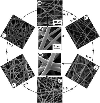 | ||
| Fig. 1
SEM images of PMMA ES mats with different epoxy content. a–f) The ratios of epoxy:PMMA are 0:1, 1:50, 1:10, 1:5, 1:4, 1:3, respectively. g, h) Typical enlarged SEM image of a) and b), and c) and d), respectively. Experimental parameters are: PMMA concentration 10 wt%, voltage 25 kV, work distance 15 cm, ES time 5 min. a–f) and g–h) share the same scale bars, respectively. | ||
The formation of junctions is also applicable to other polymers, such as polystyrene (PS). We carried out ES of PS solutions containing different amounts of epoxy. The concentration of PS was 20 wt%, and the other experimental parameters were the same as for PMMA. It was not surprising that we observed no junctions in the pure PS ES mats [Fig. 2a)]. Similar to PMMA, too small an amount of epoxy (such as E/P 1:10) did not produce junctions [Fig. 2b) and e)]. When the amount of epoxy added was E/P 1:5, junctions formed [Fig. 2c) and f)]. Excessive amounts of epoxy resin (such as E/P 1:2) also made ESPS fibers adhere together and ES mats could not keep the shape of individual fibers [Fig. 2d)].
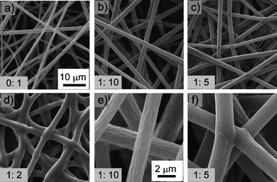 | ||
| Fig. 2
SEM images of PS ES mats with different epoxy content. a–d) The ratios of epoxy:PS are 0:1, 1:10, 1:5, 1:2, respectively. e, f) Typical enlarged SEM image of b) and c), respectively. Experimental parameters are: PS concentration 20 wt%, voltage 25 kV, work distance 15 cm, ES time 5 min. a–d) and e–f) share the same scale bars, respectively. | ||
We further tested the influence of other experimental parameters on the formation of junctions, such as applied voltage, work distance, and concentration of PMMA solutions. In the first experiment, we varied the applied voltages from 15 to 25 kV. The second was to set the work distance at 9, 12 and 15 cm, respectively. In the last experiment, we prepared PMMA/epoxy solutions with different PMMA concentrations, i.e., 6%, 8%, 10% and 12%. These three experiments indicated that voltage, work distance and PMMA concentration had negligible influence on the formation of junctions.
Except for SEM, no effective methods were addressed to evaluate junctions.13,14 We therefore developed two new methods to confirm the formation and qualitatively evaluate the performance of these junctions. First, we applied the water contact experiment. We performed the experiment using conventional contact angle equipment. We first generated a water drop (about 0.5 μL) on the orifice of a needle tip. The surface of the ES mat was then carefully moved upward to approach the water drop at a speed of about 1 mm s−1. After the surface came in contact with the water drop, we withdrew the ES mat away from the water drop at the same speed. The results of water contact experiment on PMMA (without junctions) and PMMA/epoxy (with junctions) ES mats were clearly different. In Fig. 3a), when the distance between the water drop and the surface of the PMMA ES mat was about 10 mm, nanofibers flew from the ES mats to adhere to the water drop due to the electrostatic interaction between the water drop and the nanofibers (Fig. 3a),0 s). More and more nanofibers adhered to the water drop when the PMMA ES mat was moved closer to water drop. The contact angle was estimated to be about 143° due to the hydrophobicity of PMMA ES mats when the water drop fully contacted the surface (i.e., static contact angle). Interestingly, the strong interactions between the water drop and the ES mat drove nanofibers to move with water drop (Fig. 3a),10 s and 20 s) when withdrawing the ES mat from the water drop. As a result, the surface of the ES mat was damaged because of weak/no entanglements between the nanofibers. In contrast, water contact experiment on ES mats of PMMA/epoxy did not damage the mat surface because junctions between the nanofibers formed a stable 3D network [Fig. 3b)]. The visually dynamic process of water contact experiment was showed in movies 1 and 2 of the ESI.†
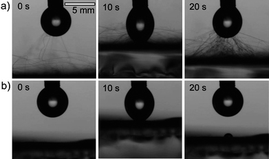 | ||
| Fig. 3 Water contact experiments on a) a PMMA ES mat and b) a PMMA/epoxy ES mat. See also movies 1 and 2 of the ESI.† | ||
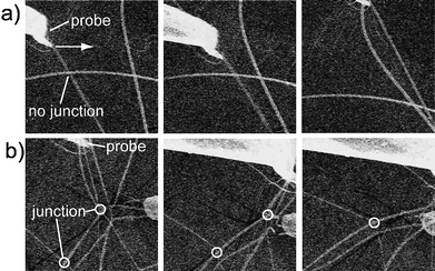 | ||
| Fig. 4 Micro-manipulation experiments on a) a PMMA ES mat and b) a PMMA/epoxy ES mat. See also movies 3 and 4 of the ESI.† | ||
Second, we qualitatively evaluated the performance of the junctions via micro-manipulation. A pair of micro-manipulators with a sharp tip was set inside the SEM. The probe could be moved in 3D space under the controller, and thus nanofibers could be precisely handled. We specially reduced the density of deposited nanofibers on a silicon wafer for this experiment, with all other conditions constant. When probe poked PMMAnanofibers (Fig. 4a), without junctions), one fiber moved with the probe while other fibers did not move with the moving fiber because there were not enough interactions between fibers. However, because junctions existed between nanofibers in the PMMA/epoxy ES mats, all the fibers moved together with the probe [Fig. 4b)]. The visually dynamic process of the micro-manipulation experiment is shown in movies 3 and 4 of the ESI.† Thus, both the water contact and micro-manipulation experiments confirmed the formation of junctions for nanofibers produced from epoxy and PMMA blends, and these junctions led the ES mats to form stable 3D networks.
In conclusion, we have reported a simple yet effective method that uses epoxy as an adhesive material to produce junctions between nanofibers. Other adhesive materials could be applied to comply to the needs of different ES solutions as well as their different applications. Junctions between nanofibers improve the stability of ES mats. This improved stability is critical in many applications, such as to enhance the performance of ES mats being used as integrative membranes in filtration,15 tissue engineering16 and substrates for immunoassay ,3etc. Although the water contact and micro-manipulation experiments are only qualitative, the results of these two new methods are obvious and convincing, so they will be widely applicable methods to evaluate the mechanical performance of materials assembled from building blocks at the micro- or nano-scale.
This project was supported by the National Science Foundation of China (20904037), the 100 Talents Program of CAS (08BM031001), and the Natural Science Foundation of Jiangsu Province (BK2009141). We thank the Public Center for Characterization and Test at SINANO.
References
- H. D. Tran, D. Li and R. B. Kaner, Adv. Mater., 2009, 21, 1487 CrossRef CAS.
- Y. N. Xia, P. D. Yang, Y. G. Sun, Y. Y. Wu, B. Mayers, B. Gates, Y. D. Yin, F. Kim and Y. Q. Yan, Adv. Mater., 2003, 15, 353 CrossRef CAS.
- D. Y. Yang, X. Niu, Y. Y. Liu, Y. Wang, X. Gu, L. S. Song, R. Zhao, L. Y. Ma, Y. M. Shao and X. Y. Jiang, Adv. Mater., 2008, 20, 4770 CrossRef CAS.
- E. Formo, E. Lee, D. Campbell and Y. N. Xia, Nano Lett., 2008, 8, 668 CrossRef CAS.
- J. Doshi and D. H. Reneker, J. Electrost., 1995, 35, 151 CrossRef CAS.
- D. Li and Y. N. Xia, Adv. Mater., 2004, 16, 1151 CrossRef CAS.
- A. Greiner and J. H. Wendorff, Angew. Chem., Int. Ed., 2007, 46, 5670 CrossRef CAS.
- D. Y. Yang, B. Lu, Y. Zhao and X. Y. Jiang, Adv. Mater., 2007, 19, 3702 CrossRef CAS.
- Y. Zhao, X. Y. Cao and L. Jiang, J. Am. Chem. Soc., 2007, 129, 764 CrossRef CAS.
- Z. Y. Li, H. N. Zhang, W. Zheng, W. Wang, H. M. Huang, C. Wang, A. G. MacDiarmid and Y. Wei, J. Am. Chem. Soc., 2008, 130, 5036 CrossRef CAS.
- D. Gupta, J. Venugopal, S. Mitra, V. R. G. Dev and S. Ramakrishna, Biomaterials, 2009, 30, 2085 CrossRef CAS.
- D. H. Reneker and A. L. Yarin, Polymer, 2008, 49, 2387 CrossRef CAS.
- S. Y. Jang, V. Seshadri, M. S. Khil, A. Kumar, M. Marquez, P. T. Mather and G. A. Sotzing, Adv. Mater., 2005, 17, 2177 CrossRef CAS.
- P. Anzenbacher and J. M. A. Palacios, Nat. Chem., 2009, 11, 80 Search PubMed.
- R. Gopal, S. Kaur, C. Y. Feng, C. Chan, S. Ramakrishna, S. Tabe and T. Matsuura, J. Membr. Sci., 2007, 289, 210 CrossRef CAS.
- J. W. Xie, S. M. Willerth, X. R. Li, M. R. Macewan, A. Rader, S. E. Sakiyama-Elbert and Y. N. Xia, Biomaterials, 2009, 30, 354 CrossRef CAS.
Footnote |
| † Electronic supplementary information (ESI) available: Experimental details and supplementary movies 1–4. See DOI: 10.1039/b9nr00212j |
| This journal is © The Royal Society of Chemistry 2010 |