The new future of scanning probe microscopy: Combining atomic force microscopy with other surface-sensitive techniques, optical microscopy and fluorescence techniques
Susana
Moreno Flores
* and
José L.
Toca-Herrera
*
Biosurfaces Unit, CIC biomaGUNE, Paseo Miramon 182, San Sebastian, Spain. E-mail: smoreno@cicbiomagune.es; jltocaherrera@cicbiomagune.es
First published on 3rd September 2009
Abstract
Atomic force microscopy (AFM) is in its thirties and has become an invaluable tool for studying the micro- and nanoworlds. As a stand-alone, high-resolution imaging technique and force transducer, it defies most other surface instrumentation in ease of use, sensitivity and versatility. Still, the technique has limitations to overcome. A promising way is to integrate the atomic force microscope into hybrid devices, a combination of two or three complementary techniques in one instrument. In this way, a comprehensive description of molecular processes is at hand; morphological, (electro)chemical, mechanical and kinetic information are simultaneously obtained in one experiment. Hereby we review the recent efforts towards such development, describing the aim and the applications resulting from the combination of AFM with spectroscopic, optical, mechanical or electrochemical techniques. Interesting possibilities include using AFM to bring optical microscopies beyond the diffraction limit and also bestowing spectroscopic capabilities on the atomic force microscope.
 Susana Moreno Flores Susana Moreno Flores | Susana Moreno Flores graduated in Chemistry from the Complutense University, Madrid. This was followed by her doctorate on polymer dynamics using dielectric relaxation spectroscopy at the same university, which she finished in 2001. Between 2001 and 2003 she did postdoctoral research on the surface properties of polyelectrolyte monolayers at the Ecole Normale Supérieure, Paris. Between 2003 and 2006 she was a postdoctoral fellow at the Max-Planck Institute of Polymer Research, where she gained experienced with scanning probe microscopies in the group of Prof. H.-J. Butt. In 2007 she joined the group of José Luis Toca-Herrera at CIC biomaGUNE. |
 José L. Toca-Herrera José L. Toca-Herrera | José Luis Toca-Herrera graduated in Physics from the University of Valencia, in 1993. In 1994 he did one-year research at Max-Planck Institute of Polymer Research. From 1996 to 1999 he completed his PhD at the Max-Planck Institute of Colloids and Interfaces under the supervision of Helmuth Möhwald. He has held Postdoctoral positions at the Technical University-Berlin, the University of Cambridge, and at the Center for Nanobiotechnology (BOKU-Vienna). In June 2004, he joined the Rovira i Virgili University as Ramón y Cajal Researcher. In 2007 he moved to CIC biomaGUNE as group leader. Since June 2008 he is I3 research professor. |
AFM: blindly probing surfaces may not be enough
Deprived of our eyesight, we humans sense the objects around us with the aid of our hands or sticks. In this way we get an idea about objects' size, their shape, their texture and their hardness. As we step forward, we intuitively probe our immediate environment by systematically moving our hands or swinging a stick to the left and right, and up and down. We register the position of an obstacle and we follow its contours by just sliding or tapping our fingertips over its surface.The atomic force microscope certainly resembles the human analog as a blind microscope that can sense micro-and nano-objects (Fig. 1). Indeed, the instrument provides the probing stick, a microsized cantilever with a tip at its free end; a piezodriven device to move the probe over the sample (or vice versa) in three dimensions with nanometre precision; a means to get the tip position during its movement and a feedback mechanism to control how strongly the tip slides or taps over the sample surface. In this way, atomic force microscopy (AFM) has become an invaluable technique to explore the morphology of the nanoworld. Moreover, since the cantilever is a force transducer, it has been extensively used to study surface and molecular interactions.
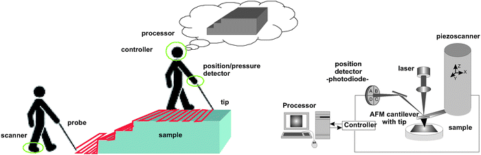 | ||
| Fig. 1 AFM imaging basics as a blind microscope analog. By blindly inspecting an object just underneath we systematically move our body and stick right and left, and up and down. We can either slide or tap our stick over the surface. Our brain controls the movement and the force we exert on the surface through our hand and stick. AFM resembles the analog with a cantilever as an elastic stick, a piezoscanner that moves it along three dimensions, a laser, and a position detector that registers its position. The ways the tip can scan the surface are more numerous than we humans have, however, on most occasions the tip is either made to slide over the surface, impinging a defined force (contact mode imaging) or to tap the sample more or less gently (intermittent contact imaging). The operation is electronically controlled to ensure the scanning is being executed under the desired scan conditions. Finally, a computer processor presents the result as an image. (From ref. 31). | ||
In spite of its many advantages, the atomic force microscope as a stand-alone tool retains some limitations. Spectroscopic identification is beyond its reach, as are determination of contact areas or absolute distances between probe and sample. Combining the atomic force microscope with complementary techniques to build hybrid instrumentation promises more than one way to overcome these limitations. Synergy may result from such combinations. Optical microscopy bestows on AFM the eyes for precise tip positioning in microstructured materials or cells; interferometry confers the capability of measuring absolute distances, and Raman spectroscopy, the label-free chemical identification of species. Reciprocally, AFM coupled with model-based techniques such as ellipsometry, surface plasmon resonance or even quartz crystal microgravimetry is of invaluable assistance in model validation, the calculation of adsorbed mass, the estimation of trapped solvent or assessing the effect of sample heterogeneity. We will briefly summarize the state-of-the-art developments of such combined techniques.
AFM + optical microscopy
Applying light microscopy to the blindatomic force microscope has turned out to be a great breakthrough in the applicability of the latter, especially in the field of biosciences. In particular, the combination of the two techniques has made it possible to investigate cellular processes in an unprecedented way, defying conventional biological practice.27 With the aid of light microscopy, precise positioning of the AFM tip into the region of interest of microsized objects such as particles or cells is possible, especially after the introduction of technologies that allow the accurate overlay of optical images and tip lateral displacements. Using transparent substrates, AFM imaging has been combined with the family of transmitted light optical microscopies such as phase and differential interference contrast (DIC), fluorescence, confocal laser scanning microscopy (CLSM), total internal reflection fluorescence (TIRF) and fluorescence lifetime imaging microscopy (FLIM). Recent implementation of AFM with upright microscopes has enabled the extension of the application of the combined techniques and epifluorescence to non-transparent substrates and hence to a wider range of materials.28 Last but not least, micro- and nanointerferometric techniques based on transmitted light microscopy such as reflection interference contrast microscopy (RICM), are particularly useful when combined with AFM. Indeed, RICM provides complementary information such as absolute tip–substrate distances and contact areas, which the AFM as a stand-alone device cannot produce.Modification of the AFM setup to be coupled to an inverted or an upright microscope requires the creation of a obstacle-free optical path to the AFM cantilever and the substrate to be analyzed (Fig. 2). Thus, the configuration of cylindrical piezoscanners mounted upright on tips or on samples is avoided. In particular, tip-scannable atomic force microscopes are preferable when simultaneous optical and AFM imaging is required. In the case of inverted microscopes, a considerable effort in AFM design is needed so as to accommodate optical condensers of high numerical aperture (0.55) without compromising the quality of optical imaging or instrument stability.
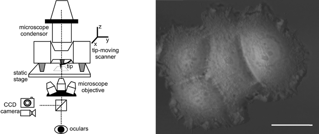 | ||
| Fig. 2 Left: Scheme of the combination of a transmitted light inverted optical microscope with the AFM. To ensure simultaneous optical and AFM imaging, the AFM tip is allowed to move in three dimensions on a static stage. Right: Optical and AFM image overlay of a breast cancer cell cluster (MCF7). Bar = 25 μm. Vertical scale of the AFM image from grey to white: 10 μm (author's contribution). | ||
AFM-CLSM
Combining confocal and atomic force microscopy on fluorescently labelled samples has become a unique tool in imaging molecular complexes on cellular surfaces at high resolution.27 The confocal microscope makes use of coherent laser illumination and an optical pinhole system to extract fluorescence images from different focal planes. As a result, the sensitivity and image quality is very much improved with respect to conventional fluorescence microscopy. Cell organelles can be selectively labelled using standard immunolabelling, and colocalized with the 3D topological images provided by the atomic force microscope (Fig. 3, left). Morphological studies on focal adhesion structures are an example of a successful combination of high-resolution imaging with fluorescence mutilabelling to ascertain the localization of interacting molecules within protein complexes12 (Fig. 3, right).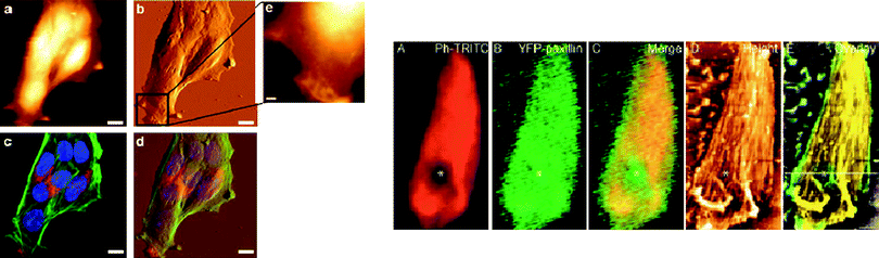 | ||
| Fig. 3 Left: Combined AFM and confocal imaging of mouse embryonic fibroblast. (a) and (b) are AFM topography and deflection images; (c) confocal imaging of cells exhibiting fluorescently labelled organelles (blue, nuclei; green: actin filaments; red: clathrin); (d) overlay of confocal and AFM imaging (reproduced from ref. 27 with kind permission from Springer Science + Business Media). Right: High-resolution imaging of focal adhesion points of de-roofed cells, with actin labelled in red (A) and YFP-paxillin (B, green). The partial disruption of the architecture is shown in the AFM (D) and f-actin-labelled confocal image, but not in the paxillin image, indicating that paxillin localization is more proximal to the focal adhesion while f-actin is localized beyond in the membrane-distal half. (From ref. 12, reproduced with permission of the Journal of Cell Science). | ||
AFM-TIRF
TIRF profits from the evanescent wave generated at a surface by a totally reflected light source. This evanescent wave, which is physically identical to that which excites plasmons on metallic surfaces, extends a few tens of nanometres along the surface normal. The wave is capable of exciting fluorophores, which is of particular advantage, since only those in close proximity to the substrate can be excited. As a consequence, a fluorescence image of the immediate vicinity of the substrate can be obtained.An interesting application of the combined AFM-TIRF technique has been applied to live cells. Cells adhere to affinity substrates by developing so-called focal adhesion points, arrangements of proteins that act as anchors. TIRF microscopy (TIRFM) can map the location of these adhesion points while the AFM cantilever exerts forces on certain cell positions. In this way, force transmission from the apical membrane to the basal membrane of cells has been detected from variations in the number and arrangement of focal adhesion points in TIRFM images.29 At the molecular level, TIRFM and AFM have been successfully correlated to ascertain the morphology of myosin self-assembled filaments in a recent study3 (Fig. 4).
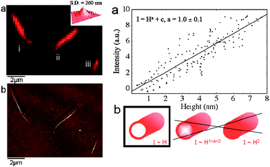 | ||
| Fig. 4 Left: TIRFM (a) and AFM (b) images of three miosin filaments. (AFM image obtained in intermittent contact mode). The inset of (a) shows the optical microscope point spread function (Gaussian fitting, standard deviation = 260 nm). Right: TIRF intensity as a function of the height measured by AFM. The intensity is a linear function of the height, which indicates that the fluorophores, situated at the heads of the myosin molecules are arranged around the filament, instead of being embedded. (Reproduced from ref. 3 with permission from Elsevier). | ||
AFM-FLIM
This promising combination of techniques has been rather poorly exploited, although it was first reported and applied in 2002.17,22 The setup shares common features with that of AFM-CLSM,17 and it has mainly been applied to fluorescent nanospheres, labelled DNA17 and live bacteria.30 Lifetimes of fluorophores attached to molecules or spheres can, however, be altered, which makes the interpretation of data particularly difficult. In particular, the presence of the AFM tip—typically Ag or Au metal-coated—can either induce fluorescence quenching or fluorescence enhancement, which may change lifetimes as well as fluorescence intensity. The net effect of these two opposing factors is not possible to predict to date.AFM-RICM
Combining these two techniques is especially advantageous when studying surface interactions and mechanics.15AFM as a dynamometer detects forces exerted between two interacting surfaces as they are being approached or separated; the force is quantified through the cantilever deflection, which behaves as a linear spring; RICM as an interferometer is capable of detecting the distance between these two surfaces with a precision on the order of 1–3 nm. To do that, light is shone on the region between the AFM probe, usually a glass bead, and the substrate. The light is reflected at both interfaces, i.e. that between the substrate and the surrounding medium and that between the medium and the probe (Fig. 5a, left). Constructive and destructive interference between the two reflected rays occurs as the tip–substrate separation varies. The interference pattern is thus a function of the tip–substrate distance, and also of the bead contour, the wavelength of the incident light and the optical properties of the medium (Fig. 5b, left). Using this combined approach, protein–ligand interactions,16,39 and microcapsule and droplet deformability9,11 have been verified (Fig. 5, right).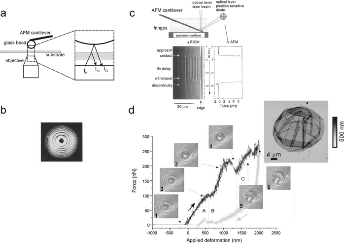 | ||
| Fig. 5 (a) AFM-RICM setup. The tip is typically a microsized (10–20 μm) glass bead attached to the cantilever. The incoming light I0 is reflected at the substrate–medium interface (I12) and at the bead–medium interface (I23). (b) The resulting interference pattern of the glass bead. From the distance and the intensity distribution of this image is it possible to calculate the glass bead profile and the bead–substrate distance (reproduced from ref. 39 with permission from Elsevier). (c) Evolution of the interference pattern while an AFM cantilever is approaching, in contact with, and withdrawing from a substrate (reproduced from ref. 16 with permission from Elsevier). The jumps and discontinuities of the AFM cantilever are visualized in RICM as fringe displacements. (d) Deformation of a polyelectrolyte multilayer capsule. The interference pattern shows the extent of deformation while the AFM exerts an ever-increasing force on the capsule (reproduced from ref. 9 with kind permission of the European Physical Journal). | ||
AFM + Raman spectroscopy: tip-enhanced Raman spectroscopy (TERS)
Introduced at the turn of the 21st century1,38 and in constant development ever since, TERS reveals itself as a powerful technique; it combines the high spatial resolution of the scanning probe microscopies with surface-enhanced Raman spectroscopy to obtain morphological and chemical information simultaneously for surface components at the nanoscale.38TERS is a near-field microscopy that makes use of an apertureless probe to enhance the Raman signal exerted by a sample. The probe is a sharp metallic (e.g., Ag or Au) tip, typically a metal-coated AFM tip or an electrochemically etched metal wire, that is irradiated along its apical axis by a low-power laser at a visible wavelength (500–650 nm). When this tip is placed sufficiently close (approx. 1 nm) to the sample, field-enhancement occurs leading to molecular excitation of the nearby sample area and thus local Raman spectra can be obtained. The mechanism of this enhancement is still an issue under discussion, however it is agreed to be intimately connected to the tip material and tip geometry and it is generally believed to have a double-nature: electromagnetic and chemical.36,38 The electromagnetic enhancement has to do with the excitation of metal plasmons at the tip apex by the laser, with the tip acting as an antenna. The generated field has a reduced spatial range and can only excite molecules that are 1–20 nm apart in the vertical direction and 20–50 nm apart in the lateral direction. The chemical enhancement (also called charge transfer) is based on molecular interactions between the metal tip and the sample surface that alters the spectroscopic properties of the latter. In this regard, TERS presents an additional advantage with respect to the classical bulk or surface-enhanced Raman spectroscopy (SERS) since Raman spectra can even be obtained from poor Raman scatterers, chemical specimens that otherwise exhibit very low or undetectable Raman signals.
The most common TERS setups are shown in Fig. 6. TERS can be operated either in reflection (especially convenient for non-transparent samples, Fig. 6a)33,34 or in confocal mode (Fig. 6b),36,41 which refers to its combination with optical reflection and confocal light scanning microscopes, respectively. In both cases, a p-polarized laser is focussed on the tip so that the polarization plane is kept parallel to the tip axis. Laser focussing is done by means of an optical objective (usually 50× or 60×) which is also used to collect the Raman radiation from the sample. In the reflection version a notch or edge-filter (NF or EF) is usually placed before the spectrometer to collect only the backscattered radiation (Fig. 6a). In the confocal version, an additional beam splitter (BS) and a flipping or folding mirror (FM) are placed before the spectrometer, which redirect both the laser source and the sample emission to a photomultiplier. In this way it is possible to switch rapidly between confocal imaging and Raman spectroscopy.
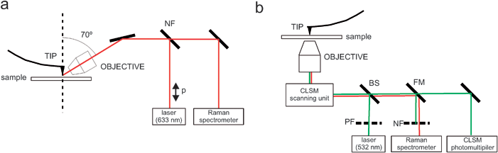 | ||
| Fig. 6 Tip-enhanced Raman spectroscopy (TERS) in reflection mode (a) and confocal mode (b). | ||
TERS has been validated through its application to model systems such as dye molecules and carbon nanotubes, which both exhibit characteristic and well-known Raman signals.33,38 As far as biomaterials are concerned, studies have been accomplished on nucleic acids and biofilms such as alginates or bacterial surfaces.36 Recently TERS has been said to be the only technique suitable for the study at the nanoscale of subsurface features of thin polymer films41 (Fig. 7, right). An important and common issue in all these studies is the achievement of a high tip-enhancement contrast, defined as the ratio of the Raman signal intensity when the tip is approached, to that when the tip is withdrawn from the sample33 (Fig. 7, left).
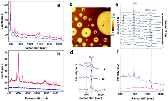 | ||
| Fig. 7 Left: Effect of tip-enhancement on the Raman spectrum of Brilliant Cresyl Blue, using (a) a gold-coated AFM tip or (b) an etched bold wire (reproduced from ref. 33 with kind permission of the European Physical Journal). Blue traces correspond to the withdrawn probe, while red traces to the engaged probe. Right: Chemical identification of film constituents. (c) AFM topography image of a blend copolymer film composed of polystyrene (PS) and polyisoprene (PI) showing circular protrusions. (d) Sequence of Raman spectra collected at the positions depicted in (c). (e) Raman spectra of pure PS and PI. (f) Magnified view of spectrum collected in background positions. Protrusions are shown to be PS-enriched, on a PI-enriched background (reproduced from ref. 41 with kind permission of the European Physical Journal). | ||
A still pending issue of TERS is finding the optimal tip preparation technique that ensures good reproducibility and high enhancement.33,41 On the other hand, the application of TERS to complex biological samples such as biofilms is still cumbersome work that involves proper spectral interpretation and makes it difficult to locate characteristic bands that are sample-specific.36 Tip-induced interference, such as carbon contaminations or far-field effects usually appear as large background signals and they should also be properly addressed.
AFM + surface plasmon resonance
Both techniques were reported to be successfully combined in the middle of the 1990s.5,37SPR is a technique that can monitor changes in the optical density of thin films on metal-coated surfaces through the excitation of surface plasmons with an incident light source. The light source typically consists of a laser of 600–700 nm wavelength that, in the most common configuration, is incident on the noble metal layer through a prism, at a range of angles that are above the critical angle where total internal reflection occurs. At a certain angle, the so-called resonance angle, excitation of the surface plasmons occurs, leading to a minimum in the reflected light. The resonance angle shifts whenever the optical density of the layer in contact with the noble metal undergoes a change, and thus it allows detection of the adsorption or desorption of molecules.The geometric complementarity of both AFM and SPR methods greatly eased the issue: the AFM needs to be mounted on top of the sample surface through a tip 3D-moving configuration, while the Kretschmann configuration of the SPR setup reaches the sample from underneath (Fig. 8, left). Coupling both techniques, it was possible to monitor in situ the kinetics of the hydrolysis of biodegradable polymer films5,37 and more recently the electropolymerization and deposition of the conductive poly(3,4-ethylenedioxythiophene) (PEDOT) on gold electrodes.2 In this work, cyclic voltammetry and potentiostatic electropolymerization were performed together with SPR to trigger the electrochemical reaction and monitor the oxidation current involved in polymer formation and deposition (Fig. 8, right).
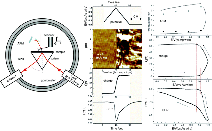 | ||
| Fig. 8 Left: Instrumental configuration for AFM + SPR. AFM and the optical setup reach the sample from above and below, respectively. SPR requires a Kretschmann configuration. Right: Simultaneous AFM, cyclic voltammetry and SPR data during the electropolymerization of PEDOT by a potential cycle from 0 to 1.2 V (reprinted with permission from ref. 2. Copyright 2006, American Institute of Physics). | ||
AFM + ellipsometry
Although not sharing all features of conventional ellipsometry, scanning near-field ellipsometric microscopy (SNEM) was first introduced in 2001 as a combination of an AFM and an ellipsometer-like setup in an attempt to characterize simultaneously the optical and non-optical properties of surfaces.20 The instrumental setup greatly resembles the AFM + SPR configuration though in this case, a polarizer, a compensator, and an analyzer are inserted in the incident and reflected light paths, respectively (Fig. 9, left).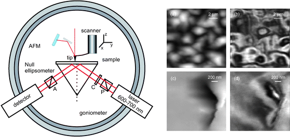 | ||
| Fig. 9 Left: Instrumental configuration for AFM + ellipsometry. Null ellipsometry requires a polarizer (P) and a compensator (C) in the laser arm and an analyser (A) in the detector arm. Right: AFM and SNEM images of a polycrystalline film of a thermotropic liquid crystal (gray scales 0–1.12 µm (a), 0–265 mV (b), 0–1.14 µm (c) and 0–42 mV in d) (reprinted with permission from ref. 20. Copyright 2001, American Institute of Physics). | ||
Ellipsometry detects the changes of polarization of incident light when it is reflected from a surface. The polarization change is expressed in the so-called ellipsometric angles, which are related to the optical properties of a thin film , i.e. thickness and refractive index, through the fundamental equation of ellipsometry.
Using metal-coated tips for the AFM and configuring the optical setup in order to produce total internal reflection on the sample backside surface, topology and SNEM images of thin polymer films were simultaneously obtained (Fig. 9, right). SNEM actually maps reflected light intensities from the sample backside surface rather than ellipsometric angles, and thus the origin of the optical contrast in the SNEM images is, to date, not fully understood.20
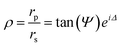
AFM + QCM
The first attempt to implement the combination of these two non-optical techniques was reported in 1998.18Quartz crystal microgravimetry relies on the vibration of a piezoelectric device (usually an AT-cut quartz slide) to detect and quantify mass deposition and changes in viscoelastic properties. The quartz crystal microbalance device can be made to oscillate by the application of an alternating electrical potential (i.e., piezodriving potential), to electrodes on the top and bottom surface of the device, producing a shear displacement on the exposed surfaces of the electrodes. Variations in the vibration frequency of the quartz device will occur as a consequence of either mass deposition or depletion upon the sensing area (usually one of the electrode surfaces), while damping in the oscillation is typically associated with material softness and/or interaction with a viscous medium, such as an aqueous solution. In particular, adsorbates on the device surface will interact with the surrounding viscous medium in a manner that is dependent on the particle size and shape. Connection of the QCM response to changes in the shape of the adsorbate or surface coverage is not straightforward. Modelling of QCM data is required, which in some cases (i.e., discontinuous adsorbate layers) is either complicated or not available.Combining the two techniques in one instrument is thus highly convenient for the interpretation of QCM data. The setup demands the simultaneous use of the QCM sensing electrode as substrate for AFM investigations (Fig. 10a). Care must be taken in the application of oscillation amplitudes, which should be below the required lateral resolution for AFM experiments.13 The coupled techniques have been applied to the study of ferritin adsorption, a quasi-spherical protein that has been shown to undergo a small deformation when adsorbed on gold. This conclusion is sustained through comparison of surface coverages obtained from AFM data, with QCM and finite element simulation data.19
 | ||
| Fig. 10 Scheme of the experimental setup. (a) Two-in-one: combined AFM and QCM; (b) Three-in-one: combined AFM, QCM and electrochemistry (also called electrochemical QCM or EQCM). The setup is compatible with either tip-moving AFM (tip on the scanner) or sample-moving AFM (sample on the scanner). RE refers to reference electrode, CE to counter electrode and WE to working electrode (substrate). Inset in (b): top-view of the substrate, showing the configuration and geometry of the electrodes. | ||
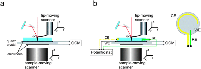
One step beyond in instrumentation involves the three-in-one versions, where the sensing substrates are also employed as working electrodes to perform in situ electrochemistry4,13,18 (Fig. 10b). Again, the simultaneous application of electrochemical (approx. 0.03 Hz) and piezodriving potentials (the latter about 4.7 MHz) is possible since both electrical signals widely differ in frequency. This modality has been proved to be particularly useful in studying the electrodeposition of metals on platinum and gold electrodes by cyclic voltammetry,4,14,18 where the ratio of frequency to damping shifts could be attributed to differences in surface roughness as a consequence of metal deposition (Fig. 11). In particular for copper electrodeposition, the mass of trapped liquid has been estimated.4
 | ||
| Fig. 11 Left column: Silver deposition on gold. Right column: Copper deposition on gold. Top image: AFM topography image showing the effects of metal deposition. Evolution of the electrochemical potential (first plot), 3rd overtone frequency and damping shifts measured with QCM (second and third plots, respectively), and current and time derivative of the frequency shift. For copper, bigger granules are deposited and the higher roughness detected with AFM may help to interpret the higher damping values obtained for this system as compared to those obtained for silver. (Reproduced with permission of ECS – The Electrochemical Society from ref. 13). | ||
AFM + Kelvin method: Kelvin probe force microscopy
Making probes conductive opens up the possibility of combining electrical and scanning probe techniques. In particular, Kelvin probe force microscopy, KPFM, combines the Kelvin method and the atomic force microscope to obtain, together with surface topography, the distribution of the contact potential difference (CPD) at nanoscale resolution.The CPD, VCPD, is the difference of the work functions of two conductive materials, which are brought into contact. The magnitude varies with temperature, but also with the presence of a third material between the contacts, such as an oxide layer, embedded dopants or adsorbed molecules.
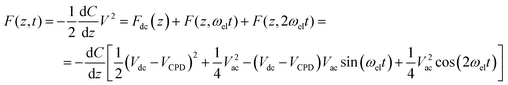
To measure the CPD an oscillatory and a bucking bias voltage are applied between the probe, a gold-,32,35 chromium/platinum-24 or a tungsten-coated tip,40 and the substrate, forming a capacitor. The ac voltage frequency, ωel, typically differs from that of the piezoinduced vibration of the cantilever for a better detection of both signals. As a consequence, the cantilever starts to oscillate. The resulting force has three different contributions, a bias and two oscillatory terms at frequencies of ωel and 2ωel, respectively, as the formula shows
![Left: Scheme of the basic principle of KPFM. A sinusoidal [Vac sin(ωelt)] and a bias voltage are applied across the sample. As a result, the tip oscillates at ωel and at 2ωel. VCPD is obtained by nulling the signal at ωel. Right: AFM image (A) and KPFM image (B) of a gap between 4 nm-thick platinum (Pd) and titanium (Ti) electrodes (substrate, SiO2/Si). (C) is a profile of the discontinuous line across the metal gap depicted in (B), showing the lateral resolution of the KPFM image as the lateral distance between the contact potentials of Pd and Ti (approximately 100 nm, reproduced with permission from ref. 10. Copyright 2007. American Chemical Society).](/image/article/2009/NR/b9nr00156e/b9nr00156e-f12.gif) | ||
Fig. 12 Left: Scheme of the basic principle of KPFM. A sinusoidal [Vac![[hair space]](https://www.rsc.org/images/entities/char_200a.gif) sin(ωelt)] and a bias voltage are applied across the sample. As a result, the tip oscillates at ωel and at 2ωel. VCPD is obtained by nulling the signal at ωel. Right: AFM image (A) and KPFM image (B) of a gap between 4 nm-thick platinum (Pd) and titanium (Ti) electrodes (substrate, SiO2/Si). (C) is a profile of the discontinuous line across the metal gap depicted in (B), showing the lateral resolution of the KPFM image as the lateral distance between the contact potentials of Pd and Ti (approximately 100 nm, reproduced with permission from ref. 10. Copyright 2007. American Chemical Society). sin(ωelt)] and a bias voltage are applied across the sample. As a result, the tip oscillates at ωel and at 2ωel. VCPD is obtained by nulling the signal at ωel. Right: AFM image (A) and KPFM image (B) of a gap between 4 nm-thick platinum (Pd) and titanium (Ti) electrodes (substrate, SiO2/Si). (C) is a profile of the discontinuous line across the metal gap depicted in (B), showing the lateral resolution of the KPFM image as the lateral distance between the contact potentials of Pd and Ti (approximately 100 nm, reproduced with permission from ref. 10. Copyright 2007. American Chemical Society). | ||
Developed as a combined technique in 199132KPFM has rapidly improved in versatility and lateral resolution. The technique was initially applied to the characterisation of metal surfaces32 at low, micrometric resolution. The application to organic films came shortly after, with the first characterizations of films of mixed amphiphilic molecules,8 self-assembled monolayers26 and a biological membrane.21 Recent years have witnessed the use of KPFM in characterising chemically lithographed self-assembled monolayers35 and the substantial increase of its lateral resolution to the submicron range. Examples of that are contact potential maps of films of pulmonary surfactants24 or gap structures in microelectrodes10 (Fig. 12). New applications of KPFM in biotechnology have abounded and developed in parallel. In these cases, KPFM is often presented as a non-destructive, label-free method for the localization and detection of proteins and nucleic acids and thus as an alternative technique to the classical fluorescence and mass spectrometric methods in proteomics.23,40Cell membrane characterization of living cells7 and single-molecule detection25 are among its most recent applications.
Conclusions
The last decade has witnessed the development of combined AFM-based techniques aimed at a more complete description of processes and structures at the nanoscale. The technical effort has been considerable, and, especially in the case of tip-enhanced techniques or the fruitful partnership with optical microscopies, the applications have been numerous and of invaluable relevance, particularly in the field of biosciences. However, the applications based on combinations of AFM with classical surface techniques such as QCM and ellipsometry have been rather scarce. Their potential is still intact though, since data interpretation remains a pending issue. Kelvin probe microscopy, still waiting for further development, open new ways to look at single molecules, membranes and cells.Acknowledgements
The authors thank the Etortek Program of the Basque Government (IE07/201) and the National Plan project (CTQ2007-66541). Uwe Rietzler and Rafael Benitez are acknowledged for providing literature references and Kathryn Melzak for grammar/spelling correction and expert advice on SPR and QCM. JLTH thanks the I3 programme of the Spanish Government.Literature
- M. S. Anderson, Appl. Phys. Lett., 2000, 76, 3130–3132 CrossRef CAS.
- A. Baba, W. Knoll and R. Advincula, Rev. Sci. Instrum., 2006, 77, 064101 CrossRef.
- A. E. X. Brown, A. Hategan, D. Safer, Y. E. Goldman and D. E. Discher, Biophys. J., 2009, 96, 1952–1960 CrossRef CAS.
- A. Bund, O. Schnedier and V. Dehnke, Phys. Chem. Chem. Phys., 2002, 4, 3552–3554 RSC.
- X. Chen, K. M. Shakesheff, M. C. Davies, J. Heller, C. J. Roberts, J. B. Tendler and P. M. Williams, J. Phys. Chem., 1995, 99, 11537–11542 CrossRef CAS.
- L.-E. Cheran, H.-D. Liess and M. Thompson, Analyst, 1999, 124, 961–970 RSC.
- L.-E. Cheran, S. Cheung, X. Wang and M. Thompson, Electrochim. Acta, 2008, 53, 6690–6697 CrossRef CAS.
- L. F. Chi, S. Jacobi and H. Fuchs, Thin Solid Films, 1996, 284–285, 403–407 CrossRef CAS.
- F. Dubreuil, N. Elsner and A. Fery, Eur. Phys. J. E, 2003, 12, 215–221 CrossRef CAS.
- S. Egger, A. Ilie, S. Machida and T. Nakayama, Nano Lett., 2007, 7, 3399–3404 CrossRef CAS.
- J. K. Ferri, P. Carl, N. Gorevski, T. P. Russell, Q. Wang, A. Böker and A. Fery, Soft Matter, 2008, 4, 2259–2266 RSC.
- C. M. Franz and D. J. Müller, J. Cell Sci., 2005, 118, 5315–5323 CrossRef CAS.
- J. M. Friedt, K. H. Choi, F. Frederix and A. Campitelli, J. Electrochem. Soc., 2003, 150, H229–H234 CrossRef CAS.
- J. M. Friedt, L. Francis, K. H. Choi, F. Frederix and A. Capitelli, J. Vac. Sci. Technol., A, 2003, 21, 1500–1505 CrossRef CAS.
- P. E. Hillner, M. Radmacher and P. K. Hansma, Scanning, 1995, 17, 144–147 CAS.
- V. Hlady, M. Pierce and A. Pungor, Langmuir, 1996, 12, 5244–5246 CrossRef CAS.
- D. Hu, M. Micic, N. Klymyshyn, Y. D. Suh and H. P. Lu, Rev. Sci. Instrum., 2003, 74, 3347–3354 CrossRef CAS.
- F. Iwata, K. Saruta and A. Sasaki, Appl. Phys. A: Mater. Sci. Process., 1998, 66, S463–466 CrossRef CAS.
- D. Johannsmann, I. Reviakine, E. Rojas and M. Gallego, Anal. Chem., 2008, 80, 8891–8899 CrossRef CAS.
- P. Karageorgiev, H. Orendi, B. Stiller and L. Brehmer, Appl. Phys. Lett., 2001, 79, 1730–1732 CrossRef CAS.
- H. F. Knapp, P. Mesquida and A. Stemmer, Surf. Interface Anal., 2002, 33, 108–112 CrossRef CAS.
- A. Kramer, W. Trabesinger, B. Hecht and U. P. Wild, Appl. Phys. Lett., 2002, 80, 1652–1654 CrossRef CAS.
- D. Laoudj, C. Guasch, E. Renault, R. Bennes and J. Bonnet, Anal. Bioanal. Chem., 2005, 381, 1476–1479 CrossRef CAS.
- Z. Leonenko, M. Rodenstein, J. Döhner, L. M. Eng and M. Amrein, Langmuir, 2006, 22, 10135–10139 CrossRef CAS.
- C. Leung, H. Kinns, B. W. Hoogenboom, S. Howorka and P. Mesquida, Nano Lett., 2009, 9, 2769–2773 CrossRef CAS.
- J. Lü, E. Delamarche, L. Eng, R. Bennewitz, E. Meyer and H.-J. Güntherodt, Langmuir, 1999, 15, 8184–8188 CrossRef.
- T. Ludwig, R. Kirmse, K. Poole and U. S. Schwarz, Pfluegers Arch., 2008, 456, 29–49 CrossRef CAS.
- S. Mangold, K. Harneit, T. Rohwerder, G. Claus and W. Sand, Appl. Environ. Microbiol., 2008, 74, 410–415 CrossRef CAS.
- A. B. Mathur, G. A. Truskey and W. M. Reichert, Biophys. J., 2000, 78, 1725–1735 CrossRef CAS.
- M. Micic, D. Hu, Y. D. Suh, G. Newton, M. Romine and H. P. Lu, Colloids Surf., B, 2004, 34, 205–212 CrossRef CAS.
- S. Moreno-Flores, in Surface Properties of Polymers, ed. C. Vasile and M. Pascu, 2007, Research Signpost, Kerala, India Search PubMed.
- M. Nonnenmacher, M. P. O'Boyle and H. K. Wickramasinghe, Appl. Phys. Lett., 1991, 58, 2921–2923 CrossRef.
- G. Picardi, Q. Nguyen, J. Schreiber and R. Ossikovski, Eur. Phys. J.: Appl. Phys., 2007, 40, 197–201 CrossRef CAS.
- D. Roy, J. Wang and M. E. Welland, Faraday Discuss., 2006, 132, 215–225 RSC.
- N. Saito, S.-H. Lee, I. Takahiro, J. Hieda, H. Sugimura and O. Takai, J. Phys. Chem. B, 2005, 109, 11602–11605 CrossRef CAS.
- T. Schmid, A. Messmer, B. S. Yeo, W. Zhang and R. Zenobi, Anal. Bioanal. Chem., 2008, 391, 1907–1916 CrossRef CAS.
- K. M. Shakesheff, X. Chen, M. C. Davies, A. Domb, C. J. Roberts, S. J. B. Tendler and P. M. Williams, Langmuir, 1995, 11, 3921–3927 CrossRef CAS.
- R. M. Stöckle, Y. D. Suh, V. Deckert and R. Zenobi, Chem. Phys. Lett., 2000, 318, 131–136 CrossRef CAS.
- J. K. Stuart and V. Hlady, Biophys. J., 1999, 76, 500–508 CrossRef CAS.
- M. Thompson, L.-E. Cheran, M. Zhang, M. Chacko, H. Huo and S. Sadeghi, Biosens. Bioelectron., 2005, 20, 1471–1481 CrossRef CAS.
- B. S. Yeo, E. Amstad, T. Schmid, J. Stadler and R. Zenobi, Small, 2009, 5, 952–960 CrossRef.
| This journal is © The Royal Society of Chemistry 2009 |