Combinatorial approaches for the identification and optimization of oxide semiconductors for efficient solar photoelectrolysis†
Michael
Woodhouse
a and
B. A.
Parkinson
*b
aThe National Renewable Energy Laboratory, 1617 Cole Blvd, Golden, CO 80401, USA
bDepartment of Chemistry and School of Energy Resources, University of Wyoming, Laramie, WY 82071, USA. E-mail: bparkin1@uwyo.edu
First published on 5th November 2008
Abstract
The cost effective generation of hydrogen with sunlight viawater photoelectrolysis is the critical breakthrough needed to transition the world to a renewable energy based hydrogen economy. A semiconductor based photoelectrolysis system may have cost advantages over using either a photovoltaic cell coupled to an electrolyzer or solar thermochemical cycles for water splitting. Unfortunately there is no known semiconducting material or combination of materials with the electronic properties and stability needed to efficiently photoelectrolyze water. Semiconducting oxides can have the required stability but present theoretical methods are insufficient to a priori identify materials with the required properties. Most likely, the discovered material will be a complex oxide containing many elements whereby each contributes to the required material properties such as light absorption across the solar spectrum, stability and electrocatalytic activity. The large number of possible multicomponent metal oxides, even if only ternary or quaternary materials are considered, points to the use of high-throughput combinatorial methods to discover and optimize candidate materials. In this critical review, we will cover some techniques for the combinatorial production and screening of metal oxides for their ability to efficiently split water with sunlight (88 references).
 Michael Woodhouse | Dr Michael Woodhouse received a PhD in Solar Energy Materials Science and Physical Chemistry under the guidance of Professor Bruce Parkinson. For his dissertation he developed the methodology to rapidly produce novel metal oxide semiconductors using inkjet printing and then test and optimize them for their ability to function as visible light driven water splitting materials in a custom-made laser scanning analysis system, as described in this review. He is currently a postdoc under Dr Brian Gregg at the National Renewable Energy Laboratory where the group is focused on the development of new materials and architectures for organic-based solar cells. Prior to graduate school he was a high school Physics and Chemistry teacher. |
 Bruce Parkinson | Bruce Parkinson received his BS in chemistry at Iowa State University in 1972 and his PhD from Caltech in 1977 under the guidance of Professor Fred Anson. After post-doctoral studies at Bell Laboratories with Adam Heller, he was a staff scientist at the Ames Laboratory, and then a senior scientist at the Solar Energy Research Institute (now the National Renewable Energy Laboratory). He joined the Central Research and Development Department of the DuPont Company in 1985. In 1991 he became Professor of Chemistry at Colorado State University until his recent departure to the Department of Chemistry and the School of Energy Resources at the University of Wyoming. His current research covers a wide range of areas including materials chemistry, UHV surface chemistry and photoelectrochemical energy conversion. |
Background
The world must eventually shift from an energy economy primarily based upon fossil fuels to one based on renewable energy sources due to the eventual depletion of fossil energy supplies and concerns about climate change due to the accumulation of carbon dioxide in the atmosphere. Sunlight is the only renewable energy source that has the potential to provide the enormous amounts of energy required by the increasing population and economic development of the world. The production and efficiency of photovoltaic solar cells that produce high value electrical energy directly from sunlight are steadily increasing, however electrical energy is not easily or economically stored. Since 75% of the world’s present energy use is in the form of fuels, methods must be developed to transform solar energy directly into storable fuels. The photoelectrolysis of water directly with sunlight is the most promising method for achieving this result. Hydrogen, the most energy dense fuel known, can be obtained from a readily available source and, when burned or used in a fuel cell, produces only water in the reversible cycle. Therefore the development of a cost-effective method for splitting water directly with sunlight would pave the way to a future hydrogen economy based on a universally accessible energy source where no pollution or greenhouse gases are produced.Current technology is capable of efficiently producing hydrogen from sunlight and water by connecting conventional solar cells to an electrolyzer.1 The major disadvantage of this approach is that both of these devices are expensive. In addition, if the electrolyzer is not located near the solar cells, losses will be incurred during transmission of the electrical power, conversion from direct current to alternating current for transmission, and the voltage step up and step down at the solar array and electrolyzer, respectively. A potentially more efficient approach is to combine these two expensive components into a single device that both absorbs the solar energy and performs the oxidation and reduction of water. In this approach the generated hydrogen can be transported through pipelines (with significantly less loss than the transport of electrical power) or in high-pressure tanks.
Although oxygen evolution was observed as early as 1968 when illuminating a rutile electrode in solution,2 application of this concept to water photoelectrolysis was first pointed out by Fujishima and Honda in a series of experiments that used the n-type semiconductor rutile form of TiO23,4 with a scheme shown in Fig. 1a. Although TiO2 is stable under illumination in aqueous electrolytes, its large bandgap (3.0 eV) limits its utilization to the UV portion of the solar spectrum and thus limits its ultimate efficiency. It should also be pointed out that the conduction band of rutile is not negative enough to reduce water and so in the original publications a “pH bias” was present where the oxygen producing side of the cell was basic with respect to the hydrogen producing electrolyte. Later work using heterojunctions of III–V materials as photoelectrodes considerably increased the visible light conversion efficiency but also increased the cost and decreased the effective lifetime of the device due to corrosion in aqueous electrolytes.5 Stability of a photoelectrolysis electrode is crucial for a viable system since the significant capital investment needed for the support structures, electrolyte handling and gas handling systems requires that the system lasts for many years. Since the photoelectrode will be continually immersed in an electrolyte and illuminated with direct solar radiation, a long lifetime is a daunting challenge that must be adequately addressed even in the basic research stages. It is primarily for their stability that metal oxide semiconductors arguably hold the most promise for constructing a stable photoelectrolysis system.
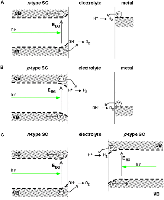 | ||
| Fig. 1 Photoelectrolysis cell configurations for the different types of semiconductors and a tandem system. In part A, a single n-type photoelectrode system capable of independently carrying out the two half-reactions without “sacrificial reagents” is shown. In B, the analogous capability is shown for a p-type photoelectrode mechanism. In C, a general two-electrode tandem concept is shown. In a stacked configuration, the larger bandgap material would be placed in front and photons with energy less than the bandgap would be transmitted to the back electrode. If they had closely matched bandgaps, the two electrodes would be placed side-by-side, allowing for full solar illumination of each (different bandgap materials could also be placed side-by-side but the module cost and size would probably increase). In either tandem configuration the photovoltages are additive but the photocurrents must be matched. Adapted from ref. 6. | ||
In addition to low cost and stability, any efficient photoelectrolysis material must also effectively utilize the solar spectrum and generate sufficient photovoltage to drive the water splitting reaction. Either a single or tandem semiconductor electrode system may be used (see Fig. 1).6 The obtained photovoltage must be greater than the thermodynamic value for the difference between the water oxidation and water reduction potentials (1.23 eV). The material(s) should have some catalytic activity for hydrogen or oxygen production so as to minimize the additional photopotential required to overcome the electrochemical overpotentials needed to drive the water oxidation and reduction reactions. Current densities (rates) on the order of 15–25 mA cm−2 with an illumination intensity around one sun are also needed for a single photoelectrode system and half these values are needed for a tandem system. In addition a single semiconductor photoelectrode must have a valence band edge that is more positive than the water oxidation potential and a conduction band edge that is more negative than the water reduction potential so that the photogenerated holes and electrons have the electrochemical driving force for the water splitting reaction. If a dual photoelectrode system is used, the conduction band of the p-type material must be negative of the water reduction potential and the valence band of the n-type material must be positive of the water oxidation potential.
As stated above either a single semiconductor electrode or a two-semiconductor electrode photoelectrolysis system can be envisioned. The single illuminated electrode system will need a bandgap greater than about 1.6 eV in order to supply the photovoltage needed for water photoelectrolysis given that a photovoltage of about two thirds the band gap is often the maximum obtainable from a good semiconductor material operating at its maximum power point. A single photoelectrode system would need to be attached to a catalytic metal (perhaps Pt) electrode that can accomplish the complementary water splitting half reaction. A two-semiconductor system, with both a p-type and an n-type semiconductor photoelectrode, can be configured in several ways. In one configuration the electrodes could be placed with the larger gap material absorbing the higher energy portion of the solar spectrum in front of the smaller band gap material of the opposite carrier type in which the wavelengths transmitted through the large band gap material would be absorbed in the smaller gap material. The two materials must absorb nearly equal numbers of solar photons since the current through each semiconductor must be matched due to the recombination at the ohmic contacts that provides the summation of the two photovoltages. Therefore in this configuration the quantum yield for water photoelectrolysis will be half that of a single photoelectrode system, however, since there is considerable photon flux in the red and near IR portion of the solar spectrum, the lower quantum yield may be offset by utilizing this portion of the solar spectrum. This configuration has the advantage that one glass substrate, with a transparent conducting layer on both sides, could be used for both materials reducing the total system costs. The ideal band gaps for the two materials have not yet been optimized but they will most likely be different than for a two-bandgap heterojunction solar cell where band gaps of 1.9 eV and 1.2 eV give the best theoretical light to electricity conversion efficiency but yield a photovoltage larger than necessary for water photoelectrolysis. Systems that convert the extra photovoltage to electrical power can also be designed but the electrical power produced would most likely be more expensive than if produced from a conventional photovoltaic device.
Another configuration would be to place the n- and p-type materials side by side rather than putting a larger band gap material in front resulting in full spectrum sunlight illumination for both electrodes. In this case an n-type and p-type electrode of the same material or two different smaller band gap materials can be paired as long as the sum of their photovoltages at maximum power was greater than the ∼1.6 eV needed for water photoelectrolysis and the photocurrents in both electrodes were matched. If two materials were used the band gaps would have to be close to each other since they need to absorb nearly the same flux of solar photons in order for the photocurrents to be matched. Two stable materials would be needed for this configuration to work, a p-type material with a conduction band at least 0.8 eV negative of both the n-type material conduction band and the hydrogen potential and valence band offsets of about 0.8 V. Two substrates would also be required, but they need not be transparent (as in the case of the stacked system discussed above) and so cheaper and more abundant materials may be utilized.
Any photoelectrolysis system will have to be designed with an ion conducting separator or electrolyte path between the two electrodes and with separate gas collection plumbing for hydrogen and perhaps oxygen. Oxidation reactions, other than water oxidation, have been discussed since there is much less demand for pure oxygen than there is for hydrogen. The commercial demand for oxygen would be rapidly saturated once any water splitting photoelectrolysis system with the capacity to produce meaningful amounts of hydrogen is deployed. The only other commercial chemical currently produced on a large scale by aqueous electrolysis is chlorine, but again the demand for chlorine would be quickly met by any system producing enough hydrogen fuel to make an impact on world energy demand. However, photoelectrolysis technology could get an initial boost from the additional revenue obtained from the photoelectrolysis of hydrochloric acid or brine.
Often materials are synthesized and tested for photochemical water splitting activity as either colloidal solutions or as powdered slurries. While this method may be useful for screening for water splitting activity, it is unlikely that homogeneous colloidal solutions or slurries will be useful for a practical water splitting system. Several reasons for this include: (1) The products are not produced in separate compartments, resulting in highly explosive mixtures of hydrogen and oxygen. (2) Energy is required to separate hydrogen and oxygen reducing the overall efficiency of the water splitting process. (3) Since catalysts for hydrogen and oxygen production from water are also good catalysts for the recombination of hydrogen and oxygen, illumination of such systems will eventually result in a photostationary state where forward and back reactions have equal rates and no more water splitting can occur. The exchange current at the photostationary state will be related to the solubility of the gases in the electrolyte and the rate at which they are removed from the reactor.
To avoid undesirable back reactions, and the poor kinetics for hydrogen or oxygen production, sacrificial reagents are often used in the photoreactors to scavenge either holes or electrons as shown in Fig. 2. The most common examples of hole scavenging agents introduced into solution are alcohols (usually methanol), amines (usually triethanolamine or EDTA) or sulfite salts. Electron scavengers such as the easily reduced Ag+ can also be added. Electron or hole scavengers can be useful to study one of the water splitting half reactions without complications associated with the kinetics of the other half reaction (although using a three electrode potentiostat to study a single photoelectrode would achieve the same end) but these additives are not viable for any practical system for sustainable energy production.
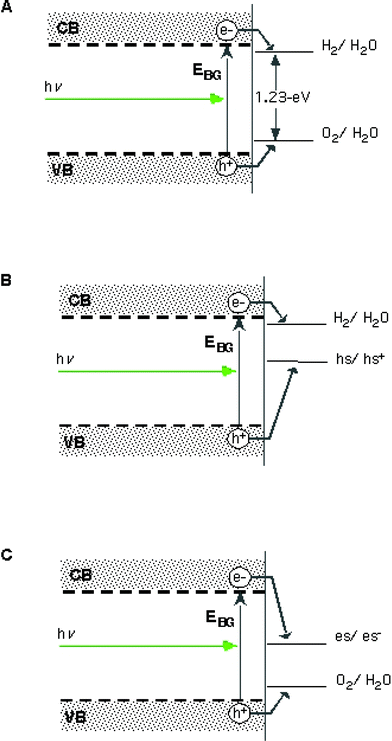 | ||
| Fig. 2 Semiconductor–electrolyte junction energetics for the water splitting half-reactions. In part A, a single photoelectrode system (generic doping type) capable of carrying out the two half-reactions is shown. No material is known to efficiently perform this process using visible light. In B, a photoelectrode system is shown for which a sacrificial “hole scavenger” such as a sulfite electrolyte or alcohol has been introduced into the system in order to study the hydrogen evolution reaction (HER) ability of the (p-type) photoelectrode. In C, a photoelectrode system is shown for which a sacrificial “electron scavenger” such as an electrolyte containing Ag+ ions has been introduced into the system in order to study the oxygen evolution reaction (OER) ability of the n-type photoelectrode. Adapted from ref. 6. | ||
As a comprehensive review of photoelectrochemical hydrogen generation7 and a recent book8 have been published on this subject, this review will concentrate on the combinatorial aspects of the search for appropriate materials for a practical device.
Survey of known materials and their photoactivity
As discussed above the positions of the conduction band and valence bands with respect to water oxidation and reduction potentials are one requirement for a water splitting photoelectrode. The positions of the valence and conduction band edges, relative to the redox potentials of water, for a variety of semiconductors are shown in Fig. 3. The compilation of the semiconductor band positions resulted from the efforts of several groups. Among the first materials to be exhaustively studied were the perovskite structure oxides SrTiO39–13 and BaTiO3.9,14,15Fig. 3 indicates that both of these materials are better suited than TiO2 for water photoelectrolysis because their conduction band edges are more negative than the water reduction potential. Unfortunately, as is also true for TiO2, their band gaps are so large (∼3.2 eV) that they also required UV light to produce photocurrent resulting in very poor solar efficiencies.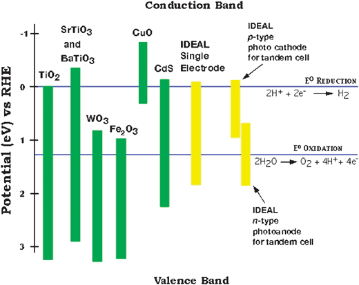 | ||
| Fig. 3 The bandgap characteristics for several known and hypothetical, ideal photoelectrolysis materials. Of the metal oxide systems shown, except for CuO, the valence band is primarily derived from O 2p orbitals—a fact that explains their relatively close valence band edges. Note that although CdS seems to match the characteristics of the ideal single material, it is unstable in aqueous electrolytes. | ||
A practical solar photoelectrolysis material must also be stable under illumination for many years while immersed in an aqueous electrolyte. Photocorrosion is the main problem with non-oxide semiconductors that have near optimum band gaps16 for efficient photocatalytic water splitting such as transition metal chalcogenides,17–19cadmium and zinc chalcogenides, GaAs,20GaP,21 and InP.22,5,23,24 Thermodynamic stability is assured only if the oxidation decomposition potential of the semiconductor is more positive than the valence band edge and the reduction decomposition potential lies more negative than the conduction band edge.25 Because the redox potentials for the decomposition reactions of these materials are generally within the band gap, and additionally because the decomposition reactions are kinetically favored, these experiments generally lead to electrode photocorrosion. If even only a tiny fraction of the photoexcited carriers are involved in photocorrosion reactions the electrode will not survive for many years under solar illumination intensities.
The most stable rocks and minerals that survive many years of weathering are all oxides, suggesting that a semiconducting oxide material will have the best chance to fulfill the stability criteria for a water splitting photocatalyst. Smaller bandgap metal oxide semiconductors, notably WO3,26–29 Fe2O3,30–35NiO,36,37 and Cu2O,38 have also been extensively studied. Although these materials harvest a larger percentage of the solar spectrum, their conduction band edge energies are often not optimally positioned for the production of hydrogen.39 They can also be difficult to electrically dope, resulting in being either poor conductors of electrons and/or holes and some of them (i.e.CuO) are still prone to corrosion.16
Examination of the oxide semiconductor band positions in Fig. 3 reveals that the conduction band positions of the plotted materials are all nearly the same and very positive. Holes at such a positive potential can easily oxidize water but waste considerable energy in doing so. One idea to both extend the spectral response of large gap oxide semiconductors and to raise the valence band energy is to incorporate sulfur, carbon or nitrogen into the lattice. A series of these compounds including Sm2Ti2S2O5,40TaON,41 Y2Ta2O5N2,42 Ta3N5,43 and LaTiO2N44,45 as well as incorporating S, N or C into TiO246–49 have recently been examined by several research groups. These groups often use density functional theory to calculate that the bottom of the conduction bands consists of empty d orbitals and, depending upon the material, the tops of the valence bands consist mainly of N 2p or S 3p orbitals resulting in smaller band gaps for improved solar energy utilization. The smaller band gaps, and fortuitous band positions relative to the redox potentials of water, mean that these materials could function as water photoelectrolysis materials; and indeed H2 and/or O2 is produced at quantum efficiencies up to 30%.41 Unfortunately, however, most of these systems are typically not reported to function without the presence of the “sacrificial reagents” in solution mentioned earlier. It is likely that the sacrificial reagents are necessary to camouflage inherent oxidation or reduction decomposition reactions and that these materials will ultimately have the same stability problems as the earlier materials that incorporated non-oxide anions since nitrogen, sulfur and carbon are easily oxidized in solution.
In principle, if one introduces an additional metal or metals into the structure that have electronegativities greater than that of the parent metal and less than that of oxygen, then it is possible that a valence band created from mixed metal d states will be more negative in energy (closer to the oxidation potential of water) than that of a pure oxygen 2p band, thereby reducing the bandgap to 1.5–2.0 eV.50 As an example, a mixed metal oxide semiconductor could be constructed with a conduction band edge derived mainly from titanium. In principle, it should then be possible to create mixed bands, lowering the band gap of the parent titanium oxide, by mixing the transition metal orbitals with the oxygen 2p orbitals. For example, the ions Mn2+, Ni2+, Cr3+, Rh3+, V4+, Os3+, Sn2+, Sb3+, Pd2+, and Pt2+ all have d orbital energies that are more positive (further down an absolute scale) than the oxidation potential of water but more cathodic than that of oxygen’s 2p orbital.50 And so, in theory at least, by combining these metals with titanium it should be possible to create a material with a band gap that can absorb a large fraction of the solar spectrum and is optimally positioned to photoelectrolyze water. Other compositions such as LuRhO3,51 SrZr0.25Ti0.75O3,50 LaVO3,52 K2La2Ti3O10,53 and RbPb2Nb3O10,54 have also been reported to be viable photoelectrolytic systems and provide useful starting points in a combinatorial search.
Combinatorial production and screening of metal oxide photocatalysts
Multicomponent materials are often required to optimize a special property. High temperature superconductivity is a good example of a special property requiring multicomponent materials. The oxide with the highest known transition temperature contains four or even five metals (HgBa2CaCu2O6+δ, Hg0.8Tl0.2Ba2Ca2Cu3O8.33, Tc≈ 125 K). Since our present theoretical knowledge is insufficient to a priori calculate the behavior of such complex systems, or estimate the identity and atomic ratios of the specific metals needed to perform the efficient photoelectrolysis of water, empirical methods will be necessary to identify the best material. Thousands, or perhaps hundreds of thousands, of mixed metal oxide photocatalyst compositions may need to be produced and tested for efficiency and corrosion resistance until an effective material is discovered. Fortunately the recent development of combinatorial methods has provided tools for the production of large libraries of compounds and the methods for screening these libraries for the presence or optimization of a property of interest. In this section we will review the combinatorial approaches that have been applied to the discovery and optimization of water splitting photocatalysts.We can first do an analysis of the number of possible combinations of mixed metal oxides that could be produced and screened. If we prepare all possible ternary oxides, mixing N materials three at a time there are N!/3!(N− 3)! permutations. Given that there are ∼50 possible candidate metals in the periodic table, this results in >19![[thin space (1/6-em)]](https://www.rsc.org/images/entities/char_2009.gif) 000 combinations to be produced and tested. If a quaternary material is needed then there are N!/4!(N− 4)! different permutations or >220000 possible combinations. It is also possible that a ternary or quaternary material will require small amounts of an additional element that acts as an electrical dopant to optimize its conductivity. These small amounts can often exist as impurities in the metal oxide precursors or may have to be discovered by additional combinatorial screening and that also multiplies the number of experiments that must be done. However, some combinations could be excluded because it would not make sense to, for example, mix only large band gap oxide materials (i.e. Ti-Zr-Si-Y oxides) and expect visible light absorption. It is clear that given the large number of possible mixtures that need to be produced, a “high throughput” approach is needed as well as multidimensional experimental design to explore the parameter space more rapidly. And while it may not be reasonable to produce and test ALL of the possible combinations, it is certainly imperative that the throughput of materials screening be rapid relative to the serial approaches that have historically been used.
000 combinations to be produced and tested. If a quaternary material is needed then there are N!/4!(N− 4)! different permutations or >220000 possible combinations. It is also possible that a ternary or quaternary material will require small amounts of an additional element that acts as an electrical dopant to optimize its conductivity. These small amounts can often exist as impurities in the metal oxide precursors or may have to be discovered by additional combinatorial screening and that also multiplies the number of experiments that must be done. However, some combinations could be excluded because it would not make sense to, for example, mix only large band gap oxide materials (i.e. Ti-Zr-Si-Y oxides) and expect visible light absorption. It is clear that given the large number of possible mixtures that need to be produced, a “high throughput” approach is needed as well as multidimensional experimental design to explore the parameter space more rapidly. And while it may not be reasonable to produce and test ALL of the possible combinations, it is certainly imperative that the throughput of materials screening be rapid relative to the serial approaches that have historically been used.
We can also use some chemical knowledge to reduce the number of combinations that need to be tested. We can very loosely classify metals into one of four categories according to their potential role in a photoelectrode material: structural, since they form very stable high heat of formation oxides (i.e.Ti, W, Zr, Ta, Si, Mo, Nb, Hf, In, Sn, Ga, Y, Sc); light absorbing, where multiple elements may be needed to absorb light across the solar spectrum55,56 (i.e.Fe, Cr, V, Co, Mn, Ni, Cu, and some rare earths such as Ce); catalytic, to lower overpotential losses in the electrochemical reactions (i.e.Ru, Rh, Pd, Ni, Pt, Ir, Os, Re);55,57,58 and ionic charge compensators (i.e. Ca, Sr, Ba, Mg, Zn, Cd, Li, Na, K, Rb, Cs)‡ that are often present in stable structures such as spinels and perovskites to balance the charge in the compound since oxygen is always present as O2−. This chemical guidance greatly reduces the number of possible combinations (but it is still in the tens of thousands). Finally, it may be necessary to deposit catalytic materials such as Pt, Pd, Ir, Ru, or Ni59–61 onto the surface of the electrode if the surface of the semiconductor has little catalytic activity.
With the appropriate substrate, a combinatorial library can be tested for photoactivity by a number of different methods. While the ideal method would be to directly measure hydrogen production with, for example, gas chromatography, the amount of hydrogen expected to be produced from a thin film photoelectrode that doesn’t absorb a large fraction of the incident light (the reason for very thin films is discussed below) is typically too small to generate hydrogen at a rate needed to overcome the solubility of the gas in aqueous solution. In light of this limitation, screening for photocatalytic activity has largely been carried out by measuring spatially resolved photocurrents or by observation of pH changes in the electrolyte near the array.
The use of pH-dependent fluorescent indicators62 or molecular sensitizers63 is based upon the principle that the local concentration of protons increases at sites catalytically active for water oxidation (oxygen production) and decreases at sites active for water reduction (hydrogen production). The reverse processes of hydrogen oxidation or oxygen reduction also cause a change in pH making the method useful for screening fuel cell catalysts as well as photoelectrolysis catalysts. A visual or CCD camera inspection of an irradiated catalyst library can be sufficient to ascertain activity if the amount of redox chemistry and/or the fluorescence of the indicator is sufficient. Otherwise, a spatial analysis of absorbance or emission changes must be carried out. The advantage of this approach is that it is a rapid detection method and avoids some of spurious signals that can result from electrochemical detection methods. On the other hand, it is not high resolution and one must assume that the indicator molecules do not interfere with the overall redox process occurring in solution (such as competitive charge transfer to the indicator in lieu of photocatalysis) and the appropriate indicator must be found for the chosen electrolyte. Alternative screening techniques with higher resolution will be described in the following section.
Methods for the combinatorial production and screening of metal oxide photocatalysts
Ink jet printing and electrochemical scanning light beam analysis
Ink jet printing has been utilized for many combinatorial chemistry applications including the production of luminescent metal oxide libraries.64 The hallmarks of ink jet printing for materials deposition are its speed, ease of use, low cost (depending upon the printing platform chosen) and its versatility. The combinatorial search strategy within our group,58 and later adopted by the Lewis group,66 utilizes ink jet printing of overlapping patterns of soluble metal oxide precursors onto a conductive substrate. Metal nitrate salts have been the most widely printed precursors since they are highly soluble and subsequent pyrolysis at temperatures below 550 °C yields metal oxides. Temperatures must be kept below about 550 °C since above these temperatures the glass begins to soften and the conducting FTO layer becomes unstable.Our work has used a research grade printer manufactured by FujiFilm Dimatix58 and off-the-shelf consumer grade printers made by Hewlett Packard.65 Originally, films were deposited in overlapping triangular gradient patterns as shown in Fig. 4. While ink jet printing such a pattern ideally produces smooth gradients in composition, in reality the extent of uneven mixing of compositions within the triangles can be unknown. Assuming that the actual deposition amounts of the material precursors is linear from the vertices to the edges of the triangle, other factors such as miscibility, phase segregation, annealing effects, etc. might also play a role and make it difficult to know the exact composition in a particular spot. One particular complication that has emerged during our studies is that the metal nitrate salts generally melt before they decompose and coalesce into droplets, resulting in less uniform films of the oxide after pyrolysis. The use of metal oxide nanoparticles, polyoxometalates and various alkoxide compounds as precursors that decompose directly into the oxide will be useful to avoid this complication.
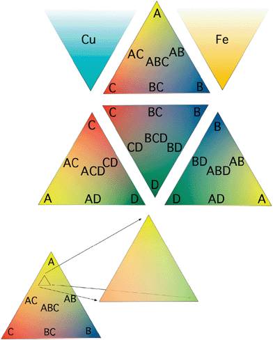 | ||
| Fig. 4 The faces of a tetrahedral 4-component phase diagram where four metals are mixed three at a time in triangles corresponding to ternary phase diagrams. When a promising composition was found, for example the small triangle inset of the ABC ternary mixture on the right, the gradients could be adjusted to expand that region of the ternary phase diagram and the necessary number of iterations could be performed until the best mixture is found. Copper oxide and iron oxide are also printed in a gradient triangle as p- and n-type simple oxide internal standards respectively. Mallouk et al. also used this scheme for the screening of precious metal fuel cell catalysts.62 | ||
To analyze for photoelectrolysis activity several groups use custom-built scanning laser screening systems where a laser is rastered over the printed and pyrolyzed substrates that are immersed in an aqueous electrolyte. A false color image of photoactivity is produced by measuring the photocurrent at each “pixel” as the laser scans over the sample. To detect small signals the laser can be chopped or modulated and a lock-in amplifier can be used to isolate the photocurrent signal even if there is substantial dark current present. A potentiostat can also be used to apply a positive or negative external bias to the sample to aid the oxidation or reduction of water, respectively. The external bias will not be useful for a practical system but is used so that a good semiconducting material that might not be catalytically active may still be identified that can have a surface catalytic layer added later.
Fig. 5 shows a template, a photograph, a false color photocurrent image and a false color photocurrent image of a compositional zoom of a promising compositional region. In the false color photocurrent images in Fig. 5, the yellow to white pixels correspond to higher relative photocurrent where a Fe-Cs-Nd composition is most photoactive. The dark blue regions represent areas where there is virtually no photoactivity either from the FTO substrate or the material. Also printed and screened using this template are n- and p-type “internal standards” of α-Fe2O3 and CuO, respectively, printed because it not only affords a direct comparison to the these well-known semiconducting oxide materials,20 but also between all printed sample plates.
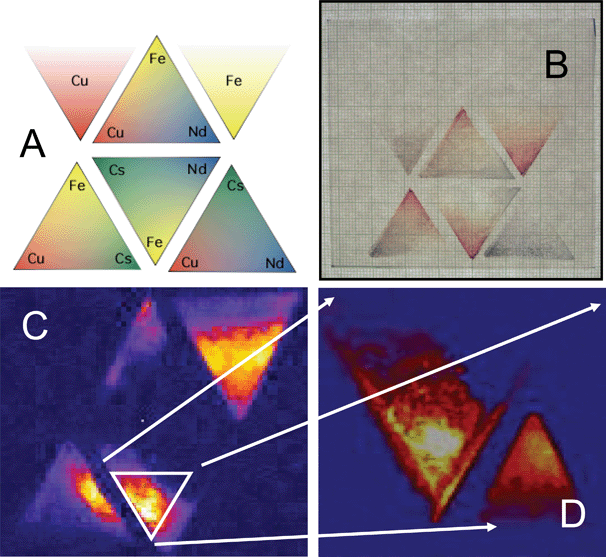 | ||
| Fig. 5 Printing and screening a four-metals-three-at-a-time pattern and a compositional zoom for a Fe-Cs-Nd-Cu system. A. False color template showing the positions and gradients used for printing the four metal precursor solutions. B. Photograph of the printed and fired film. Note the triangular internal standards of α-Fe2O3 and CuO (upper right and left, respectively) with thickness gradients (bottom to top) that are used as internal standards. C. False color photocurrent image of the film shown in B using 514.5 nm illumination under 0.5 V bias in a 0.5 M NaOH solution. The photocurrent produced at a particular “pixel”, relative to the others in the two-dimensional array, is represented by its relative brightness with the most photocurrent in a particular direction (water oxidation in this case) being the brightest. D. Photocurrent scan at 514.5 nm of a triangular composition zoom in on the brightest area of the Fe-Cs-Nd triangle shown in C that has a maximum IPCE value approximately twice that of the α-Fe2O3 internal standard (smaller triangle to the lower right). Expanding the printing gradients within the brightest region of the n-type material created the “zoom in”. Reprinted with permission from Chem. Mater., 2005, 17, 4318. Copyright 2005 American Chemical Society. | ||
Hundreds of materials have been produced and screened using the unfolded tetrahedron template, with most of the material combinations showing no or very little photoresponse but some showing significantly better performance than the internal reference materials. One of the materials discovered in our search, composed of Fe, Co, and Al, has reproducibly shown p-type photoactivity and was not previously known to function as a photoelectrolysis material. The regions of high activity were found in the Co rich regions of the Co-Al-Fe triangles. While this original high throughput method was useful for identifying promising materials, the exact stoichiometry of the metal components in the active mixture was uncertain since the exact amounts of the various “inks” delivered by the printer driver software is unknown.
In order to determine the optimum stoichiometry of the promising mixture, a series of samples with an array of areas with known compositions was prepared using a research grade ink jet printer manufactured by FujiFilm Dimatix. This printer has a camera that focuses on the printhead nozzles and software control of parameters such as the piezoelectric nozzle jetting waveform, drop spacing and volume, and jetting frequency. By controlling these parameters, production of a broad or narrow compositional range with known stoichiometries within each printed area is possible. The thickness of each sample can also be controlled with these factors or, if desired, by depositing multiple layers. An example of a sample plate prepared in this way is shown in Fig. 6. In this pattern, four different densities of Co and Fe were printed as double horizontal and double vertical rows, respectively, while different amounts of Al were deposited in a repeating pattern within groups of four squares containing identical Fe and Co amounts as shown in the dashed inset in the upper left-hand corner. The precise values of the drop spacing and density printed within each square in Fig. 6 for the Fe and Cu internal standards as well as the Fe-Co-Al oxide precursors can be found in ref. 65. As an example, the brightest square in Fig. 6, third square from the right, third row down, is given the label FeBCoDAlA which correlates to Fe1.7Co14.4Al1 (in atomic percentages 10% Fe, 84% Co, and 6% Al) and this composition was used in future photoelectrochemical and structural experiments where bulk samples were prepared as it consistently appeared to be a near optimal composition.
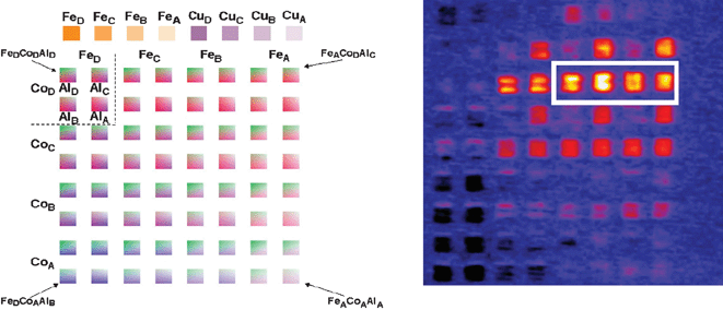 | ||
| Fig. 6 A. Printing template used for quantifying the optimal stoichiometry in the Co-Al-Fe system where known amounts of the components are printed into individual 3 mm × 3 mm squares. The density of precursor drops (and the resulting stoichiometry) corresponding to each stoichiometry for different thickness is described in ref. 58. B. False color photocurrent map with no applied bias with 532 nm laser excitation in a 0.1 M NaOH solution. The cathodic photocurrent measured by laser scanning the brightest square of the film is nearly three times that generated by the best pure CuO internal standard labeled CuD. The compositions within the solid white box were expanded in Fig. 7. Reprinted with permission from Chem. Mater., 2008, 20, 2495. Copyright 2008 American Chemical Society. | ||
In contrast to the “zoom in” shown in Fig. 5, created by adjusting the printed gradients, the most promising stoichiometries within array-based samples can be investigated much more quantitatively. To further refine the optimal composition of the photocatalyst described above, another template was created that encompasses stoichiometries outlined by the white box as well as some similar stoichiometries. The template, and the result of the photocurrent screening, is shown in Fig. 7. In this pattern the amount of cobalt was kept constant (labeled β in the figure with a drop spacing equal to that of all mixtures within the white box of Fig. 6) while the Fe and Al contents (labeled w, x, y, and z) were varied and calculated using the rationale described previously. The internal standards were printed with the same drop densities as in Fig. 6 and the overall amount of printed internal standard material relative to the working mixtures is approximately the same between Fig. 6 and 7 in order to not overestimate the contribution of sample thickness to performance. The resulting photocurrent for all working Co-Al-Fe oxides is within ±20% for all squares indicating flexibility in the stoichiometries of the photoactive compositions. Indeed, the Fe and Al content can vary by as much as a factor of two (between Co17.8Fe1Al2.1 and Co17.8Fe2.1Al1) and still produce a material with comparable photoactivity.
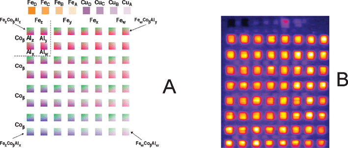 | ||
| Fig. 7 Compositional library produced by expansion of the compositional region outlined by the white box in Fig. 6. The template shown in A was created by including all of the mixtures created within the inset of Fig. 6 as well as some intermediate stoichiometries. The actual densities are shown in ref. 58, while the pure Fe and Cu internal standards were printed as in Fig. 6. B. Photocurrent map of the array of 3 mm × 3 mm squares measured in 0.1 M NaOH with a 532 nm laser showing that a rather large range of composition space appears to work better than the CuO internal standards. Reprinted with permission from Chem. Mater., 2008, 20, 2495. Copyright 2008 American Chemical Society. | ||
Currently inkjet printing allows one to rapidly produce and screen many materials and quantify the best stoichiometry. Lewis, Katz and Gingrich66 have devised a variation of the technique described above that allows for the measurement of the open-circuit photovoltage as well as the photocurrent response of each composition. The photovoltage provides a valuable estimate of the position of the quasi-Fermi level of the majority carriers under illumination, which indicates whether the photogenerated carriers are thermodynamically capable of a particular photoelectrolysis reaction. Since the photovoltage measurement is a property of the entire electrically connected substrate, to measure it for a specific composition requires electronic isolation of each metal oxide mixture, as well as passivation of the exposed conductive substrate. To achieve this up to 260 regions on the FTO substrate are laser etched to remove the FTO from the regions between the areas to be printed and electrically isolate them. Up to eight precursors are then printed in the isolated regions and pyrolyzed. An insulating epoxy is then screen printed over any exposed FTO. A multiple contact connecter is then clamped to the substrate and connected to a custom-designed printed circuit board where each contact on the circuit board is associated with a particular spot in the materials library and connected through ribbon cables to a multiplexer for the electrical measurements.
The Sayama group also currently utilizes a scanning light beam analysis system for high throughput screening of photoelectrolysis materials.67 In their system the photocurrent of each sample in an array is measured at a constant potential in a three electrode cell by scanning the photoelectrode with a focused beam from a xenon lamp guided by an optical fiber with a UV cutoff filter. The samples are produced by an automated robotic pipetting and firing protocol. Their high throughput production and screening system has been used to optimize the stoichiometry of some porous iron oxide binary compositions.
Due to the simplicity and low cost of the ink jet printing based printing and screening protocols for discovering metal oxides capable of the photoelectrolysis of water, we are embarking on a project to enlist multiple universities in the search. We have produced the first beta printing and screening kits based on inexpensive components such as Lego Midstorms® kits that were distributed in the summer of 2008 to several universities with undergraduate summer research programs. This project, funded by the Camille and Henry Dreyfus Foundation, will lay the groundwork for a new generation of young scientists dedicated to helping solve the world energy problem.
Electrochemical synthesis and screening
To our knowledge, McFarland et al. were the first to publish work on the combinatorial production of materials for water splitting. They demonstrated the electrochemical deposition of metal oxide compositions using robotics to electroplate and screen for water photooxidation activity individually created oxide materials using multiplexed photoelectrochemical cells.70 Their work focused on variations in the electrochemical synthesis conditions, surface redox catalysts, control over structure68 (by diverse surfactant and templating agents) and/or variable doping.69–71 As illustrated in Fig. 8, the electrochemical deposition system utilizes a three-electrode electrochemical cell with coiled Pt and Ag wires serving as the counter and reference electrodes, respectively, that can be moved with a computer-controlled x–y–z stage. Metal ligand systems (citrates, peroxo complexes, etc.) or electrolyte conditions (pH and relative concentrations) are carefully designed to produce similar deposition potentials for the species in solution as the precursors are electrodeposited onto the conductive substrate (FTO or Ti) surface and then connected as the working electrode for evaluation in the sample well. The desired voltage, with a necessary overpotential to ensure deposition of both species, is applied at each well until a specified amount of charge has passed before moving the scanning electrodes to the next well.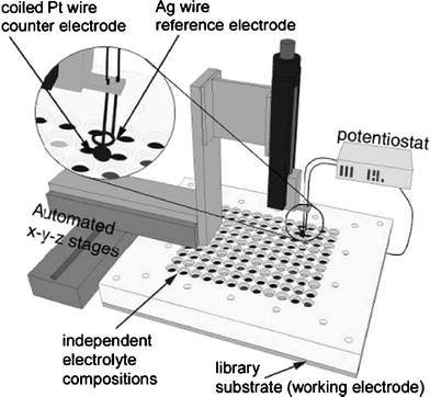 | ||
| Fig. 8 An automated electrochemical deposition system for the serial production of metal oxides. The custom made well plate shown has been designed for a 120 sample array, each sealed by “O-rings” underneath a patterned Teflon block, and each containing a unique electrolyte composition. Reprinted with permission from J. Comb. Chem., 2005, 7, 264. Copyright 2005 American Chemical Society. | ||
In this high throughput configuration each cell is manually filled using a robotic pipetter before electrodeposition. Subsequent calcination produces mixtures of known stoichiometries that were verified by XPS measurements coupled to Ar+ ion etching to examine the bulk and surface composition. Structural information was obtained with XRD. The screening system utilized for the electrochemically deposited samples incorporates measurements of flat-band potential, bias dependent photocurrent, and action spectra with a scanning photoelectrochemical probe.71 Briefly, the probe steps from sample-to-sample across the library and an automated pump fills the probe with solution from a reservoir of stock electrolyte. An illuminated optical fiber targets each individual sample well and a three-electrode configuration is used to obtain photoelectrochemical data. A monochromator is placed between a chopped Xe lamp and the optical waveguide for the IPCE measurements. Using the multiplexed photoelectrochemical screening system, the measured photoactivity of large bandgap materials for oxygen production, including ZnO69 and WO3,70 and hydrogen production, including Al2O3,72 has shown improvement after doping with certain elements around particular stoichiometries and complete photoelectrochemical information is obtained for each sample.
Sol gel routes
The recent work of Maier et al.73,74 has also added to the arsenal of combinatorial production and screening strategies to the search for novel hydrogen-producing photocatalysts, particularly for producing doped mixtures of compounds with sol gel precursors such as titanium. The reported technique incorporates computer controlled pipetting robots to quantitatively dispense stock solutions of precursors into an array of small vials. When the pipetting process is finished, the samples are placed in an orbital shaker for mixing and a consistent aging, drying, and calcination protocol is followed for each sample to produce catalyst powders. The powders are then manually ground and suspended in an aqueous methanol solution in small gas chromatography (GC) vials. After flushing the headspace within the vials with an inert carrier gas, the GC sample holder is illuminated with a visible light source and the direct production of hydrogen gas can be monitored.Using this method, after several generations of optimization a newly discovered material, Al40Bi40Pb20Ox, was identified for future studies. There are several problems associated with this technique, including the use of powders which produce hydrogen–oxygen mixtures that are difficult to separate, the use of sacrificial agents such as methanol or added water pollutants and the limitation that it does not produce uniform catalyst grain sizes. Nevertheless, it would be interesting to deploy the materials discovered by this technique as thin film photoelectrodes to test their photoelectrolysis activity.
Other thin film deposition techniques
Although it hasn’t yet been applied to the production and screening of photoelectrolysis materials, we will briefly mention some other approaches to produce metal oxide libraries using well-established thin film deposition techniques (meant here to include physical vapor deposition, sputtering, pulsed laser deposition and molecular beam epitaxy). These techniques have been used for the production of combinatorial metal oxide libraries in the search for more effective luminescent materials,75 transparent conducting oxides,76,77 and dielectrics.78,79 It would presumably be straightforward to apply the same techniques to the production of material libraries to be screened for photoelectrolysis activity.Takeuchi, Xiang, Schultz, et al. demonstrated a very elegant design for the production of a large quaternary library of metal oxide phosphors on a single substrate80 by sputtering patterns of metal oxides as shown in Fig. 9. Critical to the library design is both the alignment and power of the sputtering gun towards the target and substrate and/or the sequence of precursor depositions at different sites on a substrate using precisely machined and positioned masks. High-resolution photolithographic patterning (each site is 650 μm by 650 μm spaced 100 μm apart) is used to create the masks. After deposition of the thin films, the remaining photoresist and overlying film are washed away with acetone, leaving the sputtered materials in the unmasked regions. Each mask is used for up to four sequential depositions, with the mask rotated by 90° each time. A photograph of the luminescence of such a library produced by this method is shown in Fig. 10. The stunning array of colors was obtained by irradiating the materials with a short wavelength multiband emission UV lamp (centered around 254 nm). Clear differences in both color and intensity of the luminescence can be seen as the compositions are varied. It should be possible to extend this preparation method to produce highly controlled and precise combinatorial metal oxide libraries to be screened for photoelectrolysis activity.
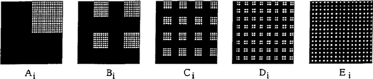 | ||
| Fig. 9 Masking scheme used to create a quaternary library of 1024 unique compositions on a single substrate. Ai, Bi, Ci, Di, and Ei represent deposition steps described in the full reference. Reprinted with permission from Science, 1998, 279, 1712. Copyright 1998 AAAS. | ||
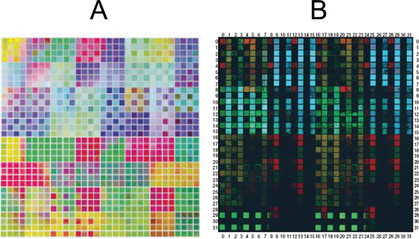 | ||
| Fig. 10 (A) Photograph of a quaternary metal oxide library produced using the masking scheme shown in Fig. 9. The total size is 2.5 cm square. (B) Photograph of the luminescence of the library under irradiation from a UV lamp. Reprinted with permission from Science, 1998, 279, 1712. Copyright 1998 AAAS. | ||
Compositional libraries of binary78 and ternary81 metal oxides have also been produced with techniques that can control layer-by-layer growth at the atomic level. These state-of-the-art thin film deposition techniques can be used to grow well-mixed compositions where the composition and thickness can be controlled at the atomic scale providing the ability to create structures such as superlattices. One such technique, dubbed combinatorial laser molecular beam epitaxy (CLMBE), has been used by Takeuchi et al.82 to produce, among other things, mixed libraries of SrTiO3. SrTiO3 is a large bandgap metal oxide that was studied early on for photoelectrolysis reactions although the group’s libraries have never been screened for photocatalytic activity.83 This tool, shown in Fig. 11, has three useful features: moving masks for quantitative control of film growth, a scanning reflection high-energy electron diffraction (RHEED) system for in situ analysis of film quality during each stage of growth, and a directed Nd:YAG laser for substrate heating, allowing for variable growth temperature as a parameter in the combinatorial library design. By monitoring the growth with RHEED, the operator can coordinate the switching of targets with mask movements to produce the desired number of the appropriate atomic-layers. Although the growth of a mixed perovskite film is shown, similar techniques can be extended to create ternary composition libraries.
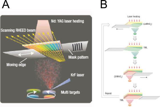 | ||
| Fig. 11 (A) Combinatorial laser molecular beam epitaxy system with in situ analysis and a substrate heating system. (B) Production scheme for continuous composition variation. The shutter between the source and substrate is moved back and forth at a controlled rate during alternate depositions of different precursor materials. With the ability to control the thickness down to a monolayer (ML), atomically controlled layer-by-layer growth can proceed by repeating for the desired number of repetitions. The illustration given is for a composition variation of the formula A1−xBxCO3 where x changes continuously across the library. Reprinted with permission from Nat. Mater., 2004, 3, 429. Copyright 2004 Nature Publishing Group. | ||
Transitioning from materials search to bulk photoelectrodes
Identification of stable semiconducting oxide materials with appropriate band gaps and band positions is only the first step towards a viable photoelectrolysis system. In general, two factors conspire to limit the photoconversion efficiency of oxide semiconductors. First the optical transitions in these materials are usually forbidden d–d transitions and so they have much lower absorption coefficients when compared to direct band gap semiconductors. The result is that light penetrates deeply into the material before being absorbed to create an electron hole pair. Other indirect photovoltaic materials such as Si have a similar absorption problem but it is overcome by having very long carrier lifetimes, resulting in long carrier diffusion lengths, so that photogenerated electrons and holes are eventually separated. Carriers in metal oxide semiconductor d-bands usually have very low mobilities due to the limited overlap between the metal d orbitals, resulting in shorter charge carrier diffusion lengths and increased bulk recombination of photogenerated carriers. Therefore, even if we could use costly single crystals of a metal oxide semiconductor, the carrier collection would be restricted to the narrow space charge layer where only a small fraction of the solar photons will be absorbed. Luckily these same two problems have been solved by the architecture of the nanocrystalline dye sensitized solar cell, that has reached laboratory efficiencies of over 10% compared to sensitized single crystals of the same oxide semiconductor that show a quantum yield of at most 1–2% due to the low light absorption of the monolayer of dye. Simply making the dye layer thicker does not solve the problem as excitons produced away from the dye/semiconductor interface recombine before they are separated due to the short exciton diffusion lengths in the organic dye layer. The high surface area morphology works to increase the effective optical absorption for these systems as the multitude of dye monolayers absorb all the light and inject their electrons into the TiO2 conduction band and the holes (or oxidized dye molecules) are quickly scavenged by a regenerator (reducing agent) in solution. A similar nanostructured morphology is probably necessary for photoelectrolysis with metal oxides in order to compensate for the low absorption and carrier mobilities characteristic of metal oxide semiconductors with forbidden d–d optical transitions.A GaP photoelectrode, with an indirect optical bandgap of 2.2 eV, provides a nice illustration of the interplay between absorption and carrier diffusion at a semiconductor/electrolyte interface. The photocurrent spectrum of a smooth single crystal of GaP has a gradual onset of photocurrent with increasing photon energy since at photon energies just above the band gap the light is penetrating deeper than both the space charge layer thickness and the carrier diffusion length. If the same GaP photoelectrode is photoelectrochemically etched, to produce a porous high surface area structure, the photocurrent spectra then shows a high carrier collection efficiency even at energies just above the indirect transition where the light penetrates many microns into the material.84,85 The high carrier collection is due to the morphology with deep pores and a high surface area such that carriers created deep in the material are still within a space charge region or within the carrier diffusion length of the semiconductor/electrolyte interface.
Another illustration of the importance of morphology in a metal oxide semiconductor uses α-Fe2O3 (hematite) as a photoelectrolysis material. Although iron(III) oxide is primarily used as a photoanode, it has been extensively studied to optimize its performance because it is inexpensive, easy to fabricate, has a bandgap (2.2 eV) that can absorb a good portion of the solar spectrum and it is stable in aqueous solutions under illumination. High surface area nanostructured morphologies86–88 of this material have been shown to more effectively harvest visible light relative to smooth films. For water cleavage, the best reported efficiencies (a solar-to-chemical conversion efficiency of 2.1%, based on the heat of hydrogen combustion, when used in a tandem configuration with a dye-sensitized solar cell) are achieved. The thickness of perpendicularly aligned α-Fe2O3 sheets is between 15 and 25 nm allowing for carrier diffusion to the surface. This morphology appears to be a critical parameter, since samples produced by different methods with similar thicknesses, crystal structure, and identical optical characteristics do not perform nearly as well. The authors argue that this particular grain size, orientation and morphology (leaf-shaped sheets) are required due to the short hole diffusion length of only a few nanometres for α-Fe2O3. This particular morphology affords facile transfer of holes to the electrolyte, before recombination occurs, while still shuttling electrons to the back contact. This morphology was produced using ultrasonic spray pyrolysis of their iron precursor solutions86 to prepare their thin films. Addition of silicon produced further improvements in photoresponse again attributed to morphology changes rather than to electronic effects.84
A nanostructured morphology also reduces the microscopic current density for water oxidation and reduction reactions resulting in lower overpotential losses than at a planer electrode. This will lower the electrocatalytic activity requirements for the semiconductor. In addition many of the cell designs discussed herein or envisioned allow for thin nanostructured films deposited on a glass substrate with a transparent conducting layer. Such a configuration allows for back illumination, much like in the nanocrystalline solar cell. Back illumination of a photoelectrolysis electrode will reduce or eliminate the efficiency losses due to light scattering by the gas bubbles being evolved from the electrode surface.
Conclusions
We have surveyed the state of water photoelectrolysis using semiconductor electrodes and can conclude that there are currently no known suitable materials to efficiently and economically carry out this process. Due to the stability requirements we surmise that semiconducting oxide photoelectrodes are required. There are many potential oxide semiconductors that need to be prepared and tested for photoelectrolysis activity and therefore high throughput combinatorial techniques are needed to discover promising materials. The first steps have been taken in the development of the combinatorial methods to solve this problem and these methods have been briefly reviewed. Optimization of the morphology of the semiconducting oxide thin film, probably with some kind of nanostructure, is required to overcome the limitations of light absorption and carrier transport in most oxide semiconductors. Mobilization of both experts and non-expert researchers to discover and optimize new semiconductor materials is needed to produce the hydrogen needed to help move towards a clean energy economy based on renewable resources.References
- M. Fisher, Int. J. Hydrogen Energy, 1986, 7, 2827.
- P. J. Boddy, J. Electrochem. Soc., 1968, 115, 199 CrossRef CAS.
- A. Fujishima and K. Honda, Bull. Chem. Soc. Jpn., 1971, 44, 1148 CAS.
- A. Fujishima and K. Honda, Nature, 1972, 238, 37 CAS.
- O. Khaselev and J. A. Turner, Science, 1998, 280, 425 CrossRef CAS.
- K. Rajeshwar, J. Appl. Electrochem., 2007, 37, 765 CrossRef CAS.
- T. Bak, J. Nowotny, M. Rekas and C. C. Sorrell, Int. J. Hydrogen Energy, 2002, 27, 991 CrossRef CAS.
- C. A. Grimes, O. K. Varghese and S. Ranjan, Light, Water, Hydrogen, Springer, 2008 Search PubMed.
- H. Kung, H. Jarrett, A. Sleight and A. Ferretti, J. Appl. Phys., 1977, 48, 2463 CrossRef CAS.
- M. S. Wrighton, A. B. Ellis, P. T. Wolczanski, D. L. Morse, H. B. Abrahamson and D. S. Ginley, J. Am. Chem. Soc., 1976, 98, 2774 CrossRef CAS.
- J. G. Mavroides, Semiconductor Liquid-Junction Solar Cells, ed. A. Heller, The Electrochemical Society, 1977 Search PubMed.
- I. Watanabe, Y. Matsumoto and E. Sato, J. Electroanal. Chem., 1982, 133, 359 CrossRef CAS.
- J. G. Mavroides, J. A. Kafalas and D. F. Kolesar, Appl. Phys. Lett., 1978, 28, 241.
- R. D. Nasby and R. K. Quinn, Mater. Res. Bull., 1976, 11, 985 CrossRef CAS.
- J. H. Kennedy and K. W. Frese, Jr, J. Electrochem. Soc., 1976, 123, 1683 CrossRef CAS.
- L. A. Harris and R. H. Wilson, Annu. Rev. Mater. Sci., 1978, 8, 99 CrossRef CAS.
- G. Hodes, S. T. Fonash, A. Heller and B. Miller, Advances in Electrochemistry and Electrochemical Engineering, ed. H. Gerischer, Wiley-Interscience, 1985 Search PubMed.
- K. Rajeshwar, P. Singh and J. Dubow, Electrochim. Acta, 1978, 23, 1117 CrossRef CAS.
- F. R. F. Fan, H. S. White, B. L. Wheeler and A. J. Bard, J. Electrochem. Soc., 1980, 127, 518 CrossRef CAS.
- A. Heller, Acc. Chem. Res., 1981, 14, 154 CrossRef CAS.
- W. H. Strehlow and E. L. Cook, J. Phys. Chem. Ref. Data, 1973, 2, 163 CAS.
- C. Levy-Clement, A. Heller, W. A. Bonner and B. A. Parkinson, J. Electrochem. Soc., 1982, 129, 1701 CrossRef CAS.
- G. C. De, A. M. Roy and S. S. Bhattacharya, Int. J. Hydrogen Energy, 1996, 21, 19 CrossRef.
- R. D. Rauh, J. M. Buzby, T. F. Reise and S. A. Alkaitis, J. Phys. Chem., 1979, 83, 2221 CrossRef CAS.
- H. Gerischer, Faraday Discuss. Chem. Soc., 1980, 70, 1A Search PubMed.
- M. Butler, R. Nasby and R. Quinn, Solid State Commun., 1976, 19, 1011 CrossRef CAS.
- M. A. Butler, J. Appl. Phys., 1977, 48, 1914 CrossRef.
- J. M. Berak and M. J. Sienko, J. Solid State Chem., 1970, 2, 109 CAS.
- H. Wang, T. Lindgren, J. He, A. Hagfeldt and S.-E. Lindquist, J. Phys. Chem. B, 2000, 104, 5686 CrossRef CAS.
- K. Hardee and A. Bard, J. Electrochem. Soc., 1976, 123, 1024 CAS.
- R. Nasby and R. Quinn, Mater. Res. Bull., 1976, 11, 985 CrossRef CAS.
- J. H. Kennedy and K. W. Frese, Jr, J. Electrochem. Soc., 1978, 125, 709 CAS.
- K. G. McGregor, M. Calvin and J. W. Otvos, J. Appl. Phys., 1979, 50, 369 CrossRef CAS.
- R. A. Frelein and A. J. Bard, J. Electrochem. Soc., 1979, 126, 1892 CrossRef.
- S. M. Wilhelm, K. S. Yun, L. W. Ballenger and N. Hackerman, J. Electrochem. Soc., 1979, 126, 419 CAS.
- M. P. Dare-Edwards, J. B. Goodenough, A. Hamnett and N. D. Nicholson, J. Chem. Soc., Faraday Trans. 2, 1981, 77, 643 RSC.
- F. P. Koffyberg and F. A. Benko, J. Electrochem. Soc., 1981, 128, 2476 CrossRef CAS.
- S. Nikitine, J. P. Zielinger, A. Coret and M. Zouaghi, Phys. Lett., 1965, 18, 105 CrossRef CAS.
- J. B. Goodenough, A. Hamnett, M. P. Dare-Edwards, G. Campet and R. D. Wright, Surf. Sci., 1980, 101, 531 CrossRef CAS.
- A. Ishikawa, T. Takata, J. Kondo, M. Hara, H. Kobayashi and K. Domen, J. Am. Chem. Soc., 2002, 124, 13547 CrossRef CAS.
- G. Hitoki, T. Takata, J. N. Kondo, M. Hara, H. Kobayashi and K. Domen, Chem. Commun., 2002, 1698 RSC.
- M. Liu, W. You, Z. Lei, G. Zhou, J. Yang, G. Wu, G. Ma, G. Luan, T. Takata, M. Hara, K. Domen and C. Li, Chem. Commun., 2004, 2192 RSC.
- G. Hitoki, A. Ishikawa, T. Takata, J. Kondo, M. Hara and K. Domen, Chem. Lett., 2002, 31, 736 CrossRef.
- A. Kasahara, K. Nukumizu, G. Hitoki, T. Takata, J. Kondo, M. Hara, H. Kobayashi and K. Domen, J. Phys. Chem. A, 2002, 106, 6750 CrossRef CAS.
- A. Kasahara, K. Nukumizu, T. Takata, J. Kondo, M. Hara, H. Kobayashi and K. Domen, J. Phys. Chem. B, 2003, 107, 791 CrossRef CAS.
- J. C. Yu, L. Zhang, Z. Zheng and J. Zhao, Chem. Mater., 2003, 15, 2280 CrossRef CAS.
- R. Asahi, T. Morikawa, T. Ohwaki, K. Aoki and Y. Taga, Science, 2001, 293, 269 CrossRef CAS.
- N. Serpone, J. Phys. Chem. B, 2006, 110, 24287 CrossRef CAS.
- S. Livraghi, M. C. Paganini, E. Giamello, A. Selloni, C. D. Valentin and G. Pacchioni, J. Am. Chem. Soc., 2006, 128, 15666 CrossRef CAS.
- G. Bin-Daar, M. P. Dare-Edwards, J. B. Goodenough and A. Hamnett, J. Chem. Soc., Faraday Trans. 1, 1983, 79, 1199 RSC.
- H. S. Jarrett, A. W. Sleight, H. H. Kung and J. L. Gillson, J. Appl. Phys., 1980, 51.
- V. Guruswamy, P. Keillor, G. L. Campbell and J. O. M. Bockris, Sol. Energy Mater. Sol. Cells, 1980, 4, 11 CrossRef CAS.
- T. Takata, K. Shinohara, A. Tanaka, M. Hara, J. Kondo and K. Domen, J. Photochem. Photobiol., A, 1997, 106, 45 CrossRef CAS.
- J. Yoshimura, Y. Ebina, J. Kondo and K. Domen, J. Phys. Chem., 1993, 97, 1970 CrossRef CAS.
- A. K. Ghosh and P. Maruska, J. Electrochem. Soc., 1977, 124, 1516 CrossRef CAS.
- H. Kato and A. Kudo, J. Phys. Chem. B, 2002, 106, 5029 CrossRef CAS.
- T. Ishii, H. Kato and A. Kudo, J. Photochem. Photobiol., A, 2004, 163, 181 CrossRef CAS.
- M. Woodhouse and B. A. Parkinson, Chem. Mater., 2008, 20, 2495 CrossRef CAS.
- I. Tsuji, H. Kato, H. Kobayashi and A. Kudo, J. Am. Chem. Soc., 2004, 126, 13406 CrossRef CAS.
- Z. Zou, J. Ye, K. Sayama and H. Arakawa, Nature, 2001, 414, 625 CrossRef CAS.
- A. Kudo and H. Kato, Chem. Phys. Lett., 2000, 331, 373 CrossRef CAS.
- E. Reddington, A. Sapienza, B. Gurau, R. Viswanathan, S. Sarangapeni, E. S. Smotkin and T. E. Mallouk, Science, 1998, 280, 1735 CrossRef CAS.
- N. D. Morris and T. E. Mallouk, J. Am. Chem. Soc., 2002, 124, 11114 CrossRef CAS.
- L. Chen, J. Bao and C. Gao, J. Comb. Chem., 2004, 6, 699 CrossRef CAS.
- M. Woodhouse, G. Herman and B. A. Parkinson, Chem. Mater., 2005, 17, 4318 CrossRef CAS.
- J. Katz, Metal Oxide Based Photoelectrochemical Cells for Solar Energy Conversion, PhD Thesis, California Institute of Technology, Pasadena CA, 2007 Search PubMed.
- T. Arai, Y. Konishi, Y. Iwasaki, H. Sugihara and K. Sayama, J. Comb. Chem., 2007, 9, 574 CrossRef CAS.
- T. F. Jaramillo, S.-H. Baeck, A. Kleiman-Shwarsctein and E. W. McFarland, Macromol. Rapid Commun., 2004, 25, 297 CrossRef CAS.
- T. F. Jaramillo, S.-H. Baeck, A. Kleiman-Shwarsctein, K.-S. Choi, G. D. Stucky and E. W. McFarland, J. Comb. Chem., 2005, 7, 264 CrossRef CAS.
- S. H. Baeck, T. F. Jaramillo, C. Brandli and E. W. McFarland, J. Comb. Chem., 2002, 4, 563 CrossRef CAS.
- T. F. Jarmillo, S.-H. Baeck, A. Kleiman-Shwarsctein, K.-S. Choi, G. D. Stucky and E. W. McFarland, J. Comb. Chem., 2005, 7, 264 CrossRef CAS.
- T. J. Jaramillo, A. Ivanovskaya and E. W. McFarland, J. Comb. Chem., 2002, 4, 17 CrossRef CAS.
- M. Seyler, K. Stoewe and W. F. Maier, Appl. Catal., B, 2007, 76, 146 CrossRef CAS.
- C. Lettmann, H. Hinrichs and W. F. Maier, Angew. Chem., Int. Ed., 2001, 40, 3160 CrossRef CAS.
- I. Takeuchi, J. Lauterbach and M. J. Fasolka, Mater. Today, 2005, 8, 18 CrossRef CAS.
- M. F. A. M. v. Hest, M. S. Dabney, J. D. Perkins, D. S. Ginley and M. P. Taylor, Appl. Phys. Lett., 2005, 87, 032111 CrossRef.
- M. F. A. M. v. Hest, M. S. Dabney, J. D. Perkins and D. S. Ginley, Thin Solid Films, 2006, 496, 70 CrossRef.
- R. B. v. Dover, L. F. Schneemeyer and R. M. Fleming, Nature, 1998, 392, 162 CrossRef CAS.
- R. B. v. Dover and L. F. Schneemeyer, Macromol. Rapid Commun., 2004, 25, 150 CrossRef.
- J. Wang, Y. Yoo, C. Gao, I. Takeuchi, X. Sun, H. Chang, X.-D. Xiang and P. G. Schultz, Science, 1998, 279, 1712 CrossRef CAS.
- R. Takahashi, H. Kubota, M. Murakami, Y. Yamamoto, Y. Matsumoto and H. Koinuma, J. Comb. Chem., 2004, 6, 50 CrossRef CAS.
- H. Koinuma and I. Takeuchi, Nat. Mater., 2004, 3, 429 CrossRef CAS.
- I. Takeuchi, private communication, 2008.
- B. H. Erné, D. Vanmaekelbergh and J. J. Kelly, J. Electrochem. Soc., 1996, 143, 305 CrossRef CAS.
- B. H. Erné, D. Vanmaekelbergh and J. J. Kelly, Adv. Mater., 1995, 7, 739 CrossRef CAS.
- I. Cesar, A. Kay, J. A. G. Martinez and M. Gratzel, J. Am. Chem. Soc., 2006, 128, 4582 CrossRef CAS.
- C. J. Sartoretti, B. D. Alexander, R. Solarska, I. A. Rutkowska, J. Augustynski and R. Cerny, J. Phys. Chem. B, 2005, 109, 13685 CrossRef CAS.
- A. Duret and M. Gratzel, J. Phys. Chem. B, 2005, 109, 17184 CrossRef CAS.
Footnotes |
| † Part of the renewable energy theme issue. |
| ‡ We purposely do not include toxic metals such as Pb, Tl, Cd and Hg since we envision eventual large-scale implementation of any discovered photocatalysts and we want to avoid the environmental consequences of these elements. |
| This journal is © The Royal Society of Chemistry 2009 |