Metal nanoparticles and their assemblies
C. N. Ramachandra Rao*a, Giridhar U. Kulkarnia, P. John Thomasa and Peter P. Edwardsb
aChemistry and Physics of Materials Unit and CSIR Centre of
Excellence in Chemistry, Jawaharlal Nehru Center for Advanced Scientific Research, Jakkur PO, Bangalore 560 064, India.. E-mail: cnrrao@jncasr.ac.in
bSchool of Chemistry, University of Birmingham, Edgbaston, Birmingham, UK B15 2TT
First published on UnassignedUnassigned11th January 2000
Abstract
Metal nanoparticles of varying sizes can be prepared by physical as well as chemical methods. They exhibit many fascinating properties, the size-dependent metal to nonmetal transition being an important one. Metal nanoparticles capped by thiols can be organized into ordered one-, two- and three-dimensional structures and these structures have potential applications in nanodevices. In this context, organization of arrays of metal nanoparticles with a fixed number of atoms assumes significance.
 C. N. Ramachandra Rao C. N. Ramachandra Rao | C. N. R. Rao is Albert-Einstein Research Professor at the Jawaharlal Nehru Centre for Advanced Scientific Research, Bangalore, India. He was a Visiting Professor at Cambridge, Cardiff and Oxford, during different periods. He is a Fellow of the Royal Society, Foreign Associate of the US National Academy of Sciences, Member of the Pontifical Academy of Sciences and Foreign Member of several academies including those of Russia and Japan. He is Honorary Fellow of the Royal Society of Chemistry and has received the Marlow Medal of the Faraday Society, the Royal Society of Chemistry Medal for Solid State Chemistry and the Einstein Gold Medal from UNESCO. He is the Centenary Lecturer of the Royal Society of Chemistry in 2000. He was President of IUPAC some years ago and is the author of over 700 papers and several books in Solid State and Materials Chemistry. |
 Giridhar U. Kulkarni Giridhar U. Kulkarni | G. U. Kulkarni received his PhD degree from the Indian Institute of Science, Bangalore and carried out post-doctoral research at Cardiff. He is a Faculty Fellow at the Jawaharlal Nehru Centre for Advanced Scientific Research, Bangalore, India. He has received the Materials Research Society of India medal. |
 P. John Thomas P. John Thomas | P. John Thomas secured his BSc degree from St. Joseph college, Trichy and is working for his PhD degree at the Jawaharlal Nehru Centre for Advanced Scientific Research, Bangalore, India. |
 Peter P. Edwards Peter P. Edwards | P. P. Edwards is Professor of Inorganic Chemistry at the University of Birmingham. He was earlier Lecturer in Chemistry and Director of the Interdisciplinary Research Centre in Superconductivity at the University of Cambridge, and Visiting Professor at Cornell University. He is a Fellow of the Royal Society and has received the Corday-Morgan, Tilden and Liversidge Medals of the Royal Society of Chemistry. He is Vice-President of the Dalton Division of Royal Society of Chemistry. He is the author of a large number of papers in Solid State Chemistry and has edited two books. |
1 Introduction
Metal nanoparticles, in the form of colloids or sols, have been used by man since the middle ages, for ornamental decoration. In the mid 17th century, Andreus Cassius discovered Purple of Cassius—a coated gold colloid, used as a pigment in glass enamel and chinaware. A few years later, Johann Kunchel perfected the technique of making ruby-coloured stained glass. In all such preparations, the brilliant colour was due to the presence of colloidal gold particles, although this fact was not recognized until the work of Michael Faraday1 in 1857. Faraday elucidated the mechanism of formation of colloidal metals and prepared stable sols and called them divided metals.† Since those early days, we have learnt much about metal nanoparticles and colloids.2 Thus, the magic numbers associated with electron angular momentum as well as nuclearity (number of atomic shells) are well established, the numbers 13, 55, 147, 309 and 561 corresponding to nuclearity of 1, 2, 3, 4 and 5 shells, respectively. Colloidal metal particles with varying sizes in the nm–μm range have been prepared in recent years by solution methods, and their morphology and geometric structures examined by microscopic techniques. It is gratifying that chemical methods of preparing metal colloids with relatively narrow size distributions have indeed met with considerable success.There has been good progress in understanding the nature of small metal aggregates.3 They cannot be simply treated as minute elements of a block of a metal, as implied by the term divided metals. This is because the conduction band present in a bulk metal will be absent and instead there would be discrete states at the band edge, as illustrated in Fig. 1. Electrons may therefore undergo quantum-confinement in very small metal particles, showing the properties of so-called quantum dots. Furthermore, a high proportion of the atoms in small metal nanoparticles will be present at the surface. The surface to bulk ratio increases markedly with the decrease in size. A nanoparticle of 10 nm diameter would have ≡10% of atoms on the surface, compared to 100% when the diameter is 1 nm.
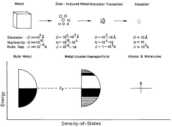 | ||
| Fig. 1 Schematic diagram showing successive fragmentation of a block of metal. The approximate diameter, nuclearity and Kubo gap of the fragments are indicated. The schematic energy level diagram alongside shows the breakdown of electronic continuum of the metal as the cluster size decreases. | ||
Metal cluster compounds have been the subject of investigation for some time.4 Of particular interest are assemblies of colloidal particles, wherein metal nanoparticles, suitably covered by organic molecules such as thiols, become self-organized in crystalline arrays of one, two or three dimensions. Such structures are of relevance to nanoelectronics of the future.5 In this article, we present the highlights of metal nanoparticles and their assemblies. In doing so, we have focussed more on those aspects which are of personal interest to us and have referred to some of the important results from the literature, quoting representative references.
2 Synthesis and geometric structure
Bare metal nanoparticles of varying sizes are prepared by employing physical methods such as evaporation of a metal in a vacuum by resistive heating, or laser ablation.6 The nanoparticles are usually deposited on a solid substrate in a vacuum. Although the size of the nanoparticles cannot be exactly controlled during evaporation, it is possible to narrow the size distribution by controlling the rate of evaporation, varying the distance between the substrate and the evaporator as well as by using nucleating inert gases. Complete control over size requires mass selection using a cluster beam apparatus. Accordingly, in the soft-landing method, nanoparticles generated in a stream of argon are made to land gently on a cold substrate covered with a bed of argon. The morphology of soft-landed nanoparticles is quite different from that obtained from direct deposition, the former being more spherical and uniform.Chemical reduction of metal salts dissolved in appropriate solvents yields small metal particles of varying size distributions.6 Since colloidal particles prepared in the solution phase have a tendency to agglomerate, it becomes necessary to protect them using surfactants or polymeric ligands such as polyvinylpyrrolidone (PVP). A variety of reducing agents have been employed for reduction. These include electrides, alcohols, glycols and certain specialized reagents such as tetrakis(hydroxymethyl) phosphonium chloride. The last reagent has enabled the preparation of gold hydrosols (down to ≡2 nm) with narrow size distributions. The polyol method has been quite popular in producing particles from nanometric to micron dimensions of a variety of metals. We show in Fig. 2 a typical SEM image of monosized gold particles prepared by the polyol method. Reverse micellar methods of preparation allow some control of the shape and size of particles.7 Other chemical methods include the sonochemical technique8 and preparations in the channels of zeolites.5 The main problem encountered in the chemical preparations pertains to the precise control over the size distribution of the colloidal particles. However, based on experience, it is possible to prepare metal colloids with reasonably narrow size distributions by varying the concentration of the metal salt, the time of reaction and related factors. Protecting agents also help to control the growth of particles. The evolution of colloidal gold particles in the nanometric regime is an activated process with a small barrier and is stochastic.9
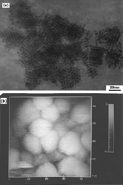
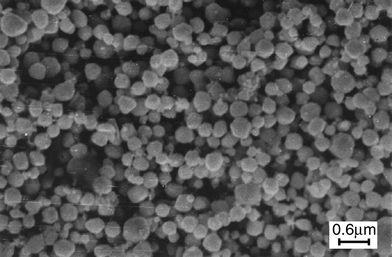 | ||
| Fig. 2 Colloidal gold particles prepared by the polyol method (from this laboratory). | ||
Real control of the size of the metal nanoparticles becomes possible when we prepare cluster compounds. Metal cluster compounds with varying metal nuclearity have been prepared,4 typical examples being [Pt38(CO)44H2]2−, Au55(PPh3)12Cl6, Cu147Se73(PEt3)22. The growth sequence of Pd clusters from a nuclearity of 4 to 561 has been examined using X-ray diffraction and other techniques.10 Other synthetic routes using PVP as the protecting agent have been explored.11 The metal nuclearities in many such compounds appear to correspond to the atomic-shell magic numbers, but there is some controversy about their exact identity. Thus, some workers have found the actual nuclearity of Au55(PPh3)12Cl6 to be different, although counter evidence has also been provided.12 Cluster compounds can be used as starting materials to generate metal nanoparticles.
High-resolution transmission electron microscopy (HREM) affords direct observation of the structures of metal nanoparticles and colloids. In Fig. 3, we show the HREM image of a gold nanoparticle along with the model and the simulated image.13 The image corresponds to that of a simple cuboctahedron. It is interesting that particles as small as 1 to 2 nm adopt the bulk structure. Some particles exhibit multiple twinning making structure elucidation more difficult. Kirkland et al.14 carried out HREM studies of a variety of metal colloids to unravel the microstructure and growth sequence. By employing HREM and other techniques, one can follow the time-dependent growth of metal nanoparticles in the solution phase.
![The single crystal cuboctahedron. (a) Hard-sphere model of the
cuboctahedron with regular hexagonal (1,1,1) facets, viewed down the
[1,1,0] axis; (b) simulated image of a cuboctahedron in the [1,1,0]
orientation with 586 atoms in the cluster and (c) TEM image of a gold
cluster with the cuboctahedron structure, viewed in a [1,1,0] orientation
(from Buffat et al.13). Reproduced
by permission of The Royal Society of Chemistry.](/image/article/2000/CS/a904518j/a904518j-f3.gif) | ||
| Fig. 3 The single crystal cuboctahedron. (a) Hard-sphere model of the cuboctahedron with regular hexagonal (1,1,1) facets, viewed down the [1,1,0] axis; (b) simulated image of a cuboctahedron in the [1,1,0] orientation with 586 atoms in the cluster and (c) TEM image of a gold cluster with the cuboctahedron structure, viewed in a [1,1,0] orientation (from Buffat et al.13). Reproduced by permission of The Royal Society of Chemistry. | ||
Besides HREM, scanning tunneling microscopy (STM) is being increasingly applied to investigate structural aspects of metal nanoparticles. STM suffers from certain disadvantages in that it cannot probe the internal structure of these aggregates; structural features are not easily discernible when the surface is covered with a surfactant. Nonetheless it is helpful in cases where the particles are unstable under intense electron beams. What would be ideal for structure determination is to carry out X-ray diffraction measurements on cluster compounds. Unfortunately, high nuclearity clusters do not crystallize. Teo et al.15 have reported the X-ray crystal structure of an Au39 cluster compound. Extended X-ray absorption fine structure (EXAFS) spectroscopy has also been used for this purpose.16 The geometry of metal clusters has been a subject of several theoretical calculations. For example, based on total energy calculations, the structural transition between icosahedral and bulk-like structures for Al clusters containing 13, 19 and 55 atoms has been examined.17 The calculations show that the cuboctahedral (bulk-like) structure becomes energetically competitive at relatively small cluster sizes. Icosahedral structures are commonly found in very small clusters.
3 Electronic structure of bare nanoparticles
The electronic structure of a metal particle critically depends on its size. For small particles, the electronic states are not continuous, but discrete, due to confinement of the electron wavefunction (see Fig. l). The average spacing of successive quantum levels, δ, known as the Kubo gap is given by δ = 4Ef/3n, where Ef is the Fermi energy of the bulk metal and n is the number of valence electrons in the nanoparticle (usually taken as its nuclearity). Thus, for an Ag nanoparticle of 3 nm diameter containing ≡103 atoms, the value of δ would be 5–10 meV. Since at room temperature kT ≅ 25 meV, the 3 nm particle would be metallic (kT > δ). At low temperatures, the level spacings, especially in small particles, may become comparable to kT, rendering them nonmetallic.2 Because of the presence of the Kubo gap, properties such as electrical conductivity and magnetic susceptibility exhibit quantum size effects.18 Discreteness of energy levels also brings about changes in the spectral features, especially those related to the valence band.High-energy spectroscopies provide direct access to the electronic structure of metal nanoparticles. In X-ray photoelectron spectroscopy (XPS), the kinetic energy of the photoelectron ejected from an atomic core-level is measured to determine the binding energy of that level. Ultraviolet photoelectron spectroscopy (UPS) and bremmstrahlung isochromat spectroscopy (BIS), on the other hand, provide information on the occupied and unoccupied levels, respectively, near Ef. In the last few years, several experiments have been carried out on nanoparticles in the desired size range obtained by the deposition of metals on amorphised graphite and other substrates, using electron spectroscopic techniques.19,20 The variation in the core-level binding energy of the metal nanoparticle with respect to the bulk metal value has been measured as a function of the coverage or particle size for metals such as Au, Ag, Pd, Ni and Cu. An important result from these experiments is that as the particle size decreases, the binding energy increases sharply by as much as 1.2 eV as in the case of Pd (Fig. 4). The variation is negligible at large coverages or particle size since the binding energies would be close to those of the bulk metals. The increase in the core-level binding energy in small particles occurs due to the poor screening of the core-hole and is a manifestation of the size-induced metal–insulator transition in nanoparticles.
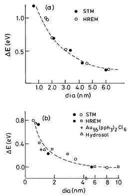 | ||
| Fig. 4 Variation of the shifts in the core-level binding energies (relative to the bulk metal value) of Pd (a) and Au (b) clusters, with the average diameter of the cluster. The diameters were obtained from HREM and STM images. In the case of Au clusters, data for a colloidal particle and a Au55 compound are also shown (from Aiyer et al.19). | ||
The electronic band structure of metal nanoparticles near the Fermi level as revealed by UPS and BIS techniques is of considerable interest.19–21 In Fig. 5 we show typical spectra of Pd nanoparticles. For large particles (≡5 nm diameter), the UP spectrum is similar to that of the bulk metal, where a considerable intensity is present at Ef due to the Pd(4d) states arising from the metallic nature of the nanoparticles. For small particles (< 2 nm diameter) however, the intensity of the 4d states at Ef decreases rapidly accompanied by a shift in the intensity maximum to higher binding energies and a narrowing of the 4d-related spectral features. The BI spectra of small nanoparticles show that the empty 4d states have negligible intensity at Ef. With the increasing particle size, new states emerge closer to Ef resembling the spectrum of the bulk metal. Thus, both UP and BI spectra establish the emergence of new states at Ef with the increase in particle size, consistent with the occurrence of an insulator-to-metal transition. Similarly, the BI spectra of Ag nanoparticles show a distinct feature which moves towards the Ef with an increase in size, accompanied by an increase in the intensity of the 5s band. All these electron spectroscopic measurements indicate that a gap manifests itself around a nanoparticle diameter of 1–2 nm possessing 300 ± 100 atoms. Recent photoelectron spectroscopic measurements21 on mass-selected Hgn nanoparticles (n = 3 to 250) reveal that the HOMO–LUMO (s–p) gap decreases gradually from ≡3.5 eV for n = 3 to ≡0.2 eV for n = 250 as shown in Fig. 6a. The band gap closure is predicted at n ≡ 400.
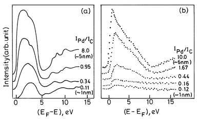 | ||
| Fig. 5 Electronic structure of small Pd clusters near the Fermi level. (a) He II UP spectra show a decrease in the intensity of the occupied 4d band with the decreasing cluster size. This is accompanied by a shift in the intensity maximum to higher binding energies and a narrowing of the spectral features. (b) BI spectra show similar effects in the empty 4d states above the Fermi level. IPd/IC values (ratios of XPS core-level intensities of Pd and the graphite substrates) are used as a measure of the coverage or the cluster size. The approximate cluster diameter is indicated in extreme cases (from Aiyer et al.19). | ||
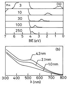 | ||
| Fig. 6 (a) Photoelectron spectra of Hg clusters of varying nuclearity. The 6p feature moves gradually towards the Fermi level, emphasizing that the band gap shrinks with increase in cluster size (from Busani et al.21). Reproduced by permission of the American Physical Society. (b) UV-visible spectra of colloidal Au particles of different mean diameter. The intensity of the plasmon band at ≡520 nm decreases with decreasing cluster size (from Sarathy et al.24). Reprinted with permission from J. Phys. Chem. B, 1997, 101, 9876. Copyright (1997) American Chemical Society. | ||
The metal–insulator transition in gaseous Hg nanoparticles has been examined by Rademann and coworkers22 by measuring the ionization energies (IE). For n < l3, the dependence of IE on n suggested a different type of bonding. A small Hg particle with atoms in the 6s26p0 configuration held together by relatively weak van der Waals forces, is essentially nonmetallic. As the nanoparticle grows in size, the atomic 6s and 6p levels broaden into bands and an insulator–metal transition seems to occur. Optical absorption spectra of mono-sized Hg nanoparticles23 of varying nuclearity in the range of 3 to 30 show an abrupt change in the spectrum from an atom-like to a plasmon-like absorption with an increase in nuclearity. Surprisingly, this occurs at n ≡8, beyond which the plasmon frequency is independent of the particle size, although the intensity shows a strong dependence. It would seem that the appearance of the plasmon band is not simply related to band gap closure, the closure generally occurring at much higher nuclearities (>100) as revealed by high energy spectroscopies. In metal colloids, surface plasmon excitations impart characteristic colors to the metal sols, the wine-red color of the gold sols being well-known. As an illustration, we show in Fig. 6b the UV-visible absorption spectra of gold sols of varying mean particle sizes.24 Colloidal particles of 4.2 and 2.1 nm diameters exhibit a distinct band around ≡525 nm, the intensity of which increases with size. The intensity of this feature becomes rather small in the case of the 1 nm diameter particles (⩽200 atoms).
Direct information on the nonmetallic gap states in nanoparticles is obtained by scanning tunneling spectroscopy (STS). This technique provides the desired sensitivity and spatial resolution making it possible to carry out tunneling spectroscopic measurements on individual particles. A systematic STS study of Pd, Ag, Cd and Au nanoparticles of varying sizes deposited on a highly oriented pyrolytic graphite (HOPG) substrate has been carried out recently under ultrahigh vacuum conditions, after having characterized the nanoparticles by XPS and STM.25 The overall slope of the current–voltage (I–V) curve near zero-bias, which is related to the density of states (DOS) near Ef, increases linearly up to a particle volume of ≡4 nm3 (≡2 nm diameter) and becomes constant for bigger particles as shown in Fig. 7a. Accordingly, the DOS in particles with a diameter >2 nm (with ≡300 atoms or more) resembles that of the bulk. Derivative spectra of bigger particles were featureless while those of the small particles (<l nm) showed well-defined peaks on either side of zero-bias due to the presence of a gap. Ignoring gap values below 25 meV (≡kT), it is seen that small particles of ⩽1 nm diameter are nonmetallic (Fig. 7b). This observation is consistent with the absence of the plasmon band in nanoparticles of 1 nm diameter (Fig. 6b). From the various studies discussed hitherto, it appears that the size-induced metal–insulator transition in metal nanoparticles (Fig. l) occurs in the range of 1–2 nm diameter or 300 ± 100 atoms.
![Scanning tunneling spectroscopy of individual metal clusters: (a)
conductance [obtained from the normalized slope of the
current–voltage (I–V) curves] as a function of cluster volume.
Above a critical volume, ≡4 nm3, the slope becomes
size-independent. (b) The conduction gap observed in small clusters of Au,
Pd, Cd and Ag as a function of cluster volume. The volume was calculated
from the cluster diameter obtained from STM (from Vinod et
al.25).](/image/article/2000/CS/a904518j/a904518j-f7.gif) | ||
| Fig. 7 Scanning tunneling spectroscopy of individual metal clusters: (a) conductance [obtained from the normalized slope of the current–voltage (I–V) curves] as a function of cluster volume. Above a critical volume, ≡4 nm3, the slope becomes size-independent. (b) The conduction gap observed in small clusters of Au, Pd, Cd and Ag as a function of cluster volume. The volume was calculated from the cluster diameter obtained from STM (from Vinod et al.25). | ||
Theoretical investigations of the electronic structure of metal nanoparticles also throw light on the size-induced changes in the electronic structure. Rosenblit and Jortner26 calculated the electronic structure of a model metal cluster and predicted electron localization to occur in a cluster of diameter ≡0.6 nm. Clusters with magic nuclearity have been extensively studied assuming cuboctahedral, octahedral and icosahedral structures. A molecular orbital calculation on an Au13 cluster27 shows that the icosahedral structure undergoes Jahn–Teller distortion while cuboctahedral does not distort. The onset of the metallic state is barely discernible in the Au13 cluster. Relativistic density functional calculations of gold clusters,28 with n = 6 to 147 show that the average interatomic distance increases with the nuclearity of the cluster. The HOMO–LUMO gap decreases with particle size from 1.8 eV for Au6 (≡0.5 nm diameter) to 0.3 eV for Au147 (≡2 nm diameter). Ab initio molecular-dynamics simulations of aluminium clusters,29 with n = 2–6, 12, 13, 55 and 147 show the minimum energy structures of Al13 and Al55 to be disorted icosahedra whereas Al147 is a near cuboctahedron. The HOMO–LUMO gap increases from ≡0.5 eV for Al2 to ≡2 eV for Al13; the gap is around 0.25 eV for Au55 and decreases to ≡0.1 eV for Aul47. The convergence of the cluster properties towards those of the bulk with an increase in size is noteworthy.
Bimetallic nanoparticles
Bimetallic or alloy colloids have been made by the chemical reduction of the appropriate salt mixtures in the solution phase. Thus, Ag–Pd and Cu–Pd colloids of varying compositions have been prepared by alcohol reduction of AgNO3 + PdOx and CuOx + PdOx mixtures.30 Ag–Pt colloids have been prepared by NaBH4 reduction of oxalate precursors and Cu–Pd colloids by thermal decomposition of acetate mixtures in high-boiling solvents. Several bare bimetallic nanoparticles have been deposited on solid substrates by thermal evaporation in a vacuum.31 Examples of such alloy nanoparticles are Ni–Cu, Ag–Au, Ni–Pd and Cu–Pd. Measurements of the core-level binding energies of the component metals in the alloy particles show that the shifts in binding energy (relative to those of bulk metals), ΔE, comprise additive contributions from alloying and the particle size. That is, the observed ΔE is given by, ΔE = ΔEalloy + ΔEsize. At large particle size, only the alloying effect, ΔEalloy, is found as in bulk alloys. Small alloy particles exhibit the size effect, in that the ΔEsize shows a marked increase with a decrease in particle size. The effect due to particle size is shown in Fig. 8 for the case of Ni–Cu alloy nanoparticles.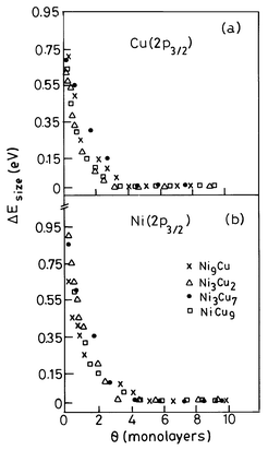 | ||
| Fig. 8 Coverage or cluster size dependence of the shift in the 2p3/2 binding energy of (a) Cu and (b) Ni in Cu–Ni bimetallic clusters (from Harikumar et al.31). | ||
4 Nanoparticle assemblies
The quest for nanoscale architecture has demanded newer synthetic methodologies for forming and organizing metal particles. In this context, the use of self-assembling surfactants is of significance. Thus, metal nanoparticles capped with thiols, silanes, phospholipids and phosphines can be prepared in solid form. We shall examine the recent results obtained with one-, two- and three-dimensional assemblies of metal nanoparticles.One-dimensional arrangements
Hornayak and co-workers32 used the ordered channels of porous alumina as templates to obtain linear arrangements of Au nanoparticles. By varying the pore size, the diameter of the nanowire could be controlled. A linear arrangement has also been obtained by coordinating Au particles (≡1.4 nm) stabilized with phosphine ligands to single stranded DNA oligonucleotide of the desired length and specific sequence.33 Organization of particles in a 1D lattice has met with limited success. There has been greater success, however, in making two-dimensional arrays.Two-dimensional arrays
Schiffrin and co-workers34 first prepared gold organosols using alkane thiols as surfactants, by phase transferring gold ions and carrying out reduction in the presence of the thiols. A novel method of thiol-derivatising hydrosols of various metals has been developed recently.35 The procedure involves mixing a hydrosol containing metal particles of the desired size distribution with a toluene solution of an alkane thiol (butanethiol or higher members). The immiscible liquid layers thus obtained are stirred vigorously with HCl or NaBH4 when the metal particles in the bottom aqueous layer gush to the upper hydrocarbon layer containing the thiol and are thiol-derivatised in this process. The completion of the derivatisation is marked by a vivid interchange of the colours from the aqueous layer to the hydrocarbon layer as demonstrated in Fig. 9. The advantage of this method is that well-characterized metal particles can be easily thiol-derivatised in a nonaqueous medium. Gold, silver and platinum particles of different sizes have been thiolised by this procedure.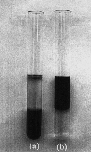 | ||
| Fig. 9 Thiol-derivatisation of a hydrosol: immiscible layers of (a) a gold hydrosol (at the bottom) and a toluene solution containing dodecanethiol (on top). (b) Thiol-derivatised Au sol in the toluene layer (on top) and the clean aqueous solution at the bottom (from Sarathy et al.35). | ||
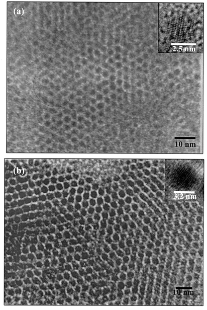
Thiolised metal nanoparticles from a nonaqueous medium are readily assembled into 2D arrays on a suitable solid substrate such as HOPG. As an example, the TEM image of a nanocrystalline array of gold particles with a mean diameter of 4.2 nm is shown in Fig. 10. The metal particles form close-packed structures extending over tens of nms with a regular spacing of ≡1 nm between them.24 The X-ray diffraction pattern of this array exhibits a low-angle peak corresponding to d spacings of 5.0 nm (Fig. 10). The distance between the particles deduced from the d spacings is somewhat smaller than that expected from the dimensions of the metal particles and the thiol, suggesting some overlap of the alkane chains of the thiols on the neighbouring particles. Ordered 2D lattices containing thiolised Au particles of two different sizes have been reported recently by Kiely et al.36 A careful study in this laboratory of 2D lattices formed by Pd nanoparticles of different sizes by employing alkane thiols of different lengths (butanethiol to hexadecanethiol) has revealed some interesting aspects of particle assemblies. Ordered 2D lattices are formed with Pd particles in the diameter range of 2 to 6 nm with octanethiol and dodecanethiol. Satisfactory 2D lattices are generally observed when the ratio of the particle diameter (d) and the thiol chain length (l) is between 1 and 4, the most ordered lattices being favoured when the d/l ratio is between 2 and 3.
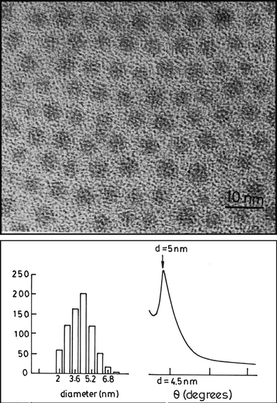 | ||
| Fig. 10 Two-dimensional array of thiol-derivatised Au particles of 4.2 nm mean diameter. Histograms indicating particle size distribution are given. XRD pattern from this array is also shown (from Sarathy et al.24). | ||
A TEM image of an array of thiol-derivatised hexagonal Pt particles (≡8 nm diameter) is shown in Fig. 11a. These particles were first prepared using an inverse micellar method, and thiol-derivatised without altering the shape or size.24 The hexagonal nanoparticles form close-packed structures resembling a honeycomb pattern. The wiggly pattern in the TEM image is due to the second layer of the honeycomb structure sitting directly over the first layer in an AB-type packing. The STM image in Fig. 11b shows three layers of the assembly. Whetten et al.37 have centrifuged and separated out fractions containing particles of different mean sizes, to prepare 2D arrays of size-selected gold particles. In another interesting experiment, Harfenist et al.38 steered a mass-selected Ag cluster beam through a toluene solution of thiol and derivatized the vacuum prepared particles. The Ag nanoparticles so prepared were stable in air and formed extended 2D arrays. It is of considerable value if one can prepare 2D lattices of metal quantum dots containing a fixed number of atoms. Langmuir–Blodgett films containing Au55 nanoparticles have been obtained.39 More interestingly, starting with cluster compounds of fixed nuclearity, it is possible to prepare the 2D lattices of thiolised Au55, Pd561 and Pd1415. In Fig. 12 we show TEM images of the 2D arrays of Pd561 and Pd1415 (ca.) obtained from cluster compounds.
 | ||
| Fig. 11 Two-dimensional array of Pt particles: (a) TEM image of thiol-derivatised Pt particles. Hexagonal particles form honeycomb-like arrays. (b) STM image showing the hexagonal stacking of the top three layers of the particles (from Sarathy et al.24). | ||
 | ||
| Fig. 12 Two-dimensional arrays of thiol-derivatised Pd clusters of definite nuclearity. TEM image of: (a) Pd561, (b) Pd1415 (ca.) obtained from the cluster compounds. Insets show lattice fringes of individual clusters (unpublished results from this laboratory). | ||
Thiol-capped metal nanoparticles provide an excellent means of studying monoelecton conduction in metal quantum dots, giving rise to the Coulomb staircase phenomenon.40,41 In Fig. 13, we show staircases obtained using gold particles of 2 and 4 nm diameter. The Coulomb gap increases with the decrease in particle size as expected. It is known that small clusters such as Au55 have a gap while Pt309 is close to the metal–insulator boundary.4l What is especially interesting is the electronic structure of 2D lattices of metal quantum dots. A 2D lattice consisting of metal nanoparticles separated a certain distance by an organic spacer serves as a model system to study the Mott–Hubbard metal–insulator transition wherein a decrease in the distance between the quantum dots (or increase in pressure) closes the Coulomb gap. By varying the interparticle distance continually in a 2D lattice of Ag particles (3 nm diameter) in a Langmuir trough, Collier et al.42 have indeed found the Coulomb gap to vanish at a critical distance. We are examining metal particles linked by conjugated thiols and dithiols of varying lengths, in comparison with those of saturated thiols.
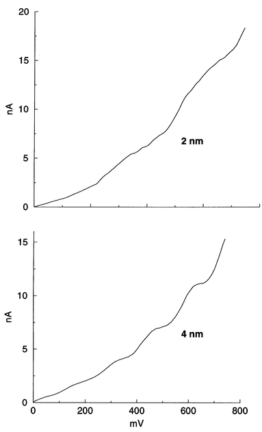 | ||
| Fig. 13 Coulomb staircase in current–voltage curves obtained employing tunneling spectroscopy on PVP covered gold nanoparticles of two different sizes (unpublished results from this laboratory). | ||
Three-dimensional superlattices
Multilayer assemblies using monothiols are generally fragile. Multilayer deposition of particle arrays is best achieved by the sequential adsorption of dithiol molecules and metal nanoparticles of the desired size, by dipping the substrate into the respective solutions with intermediate steps involving washing with toluene and drying. Using this procedure, several monometal, bimetal and metal–semiconductor superlattices have been prepared.43 The procedure is shown schematically in Fig. 14. As many as five depositions of nanocrystalline arrays could be accomplished by this method. After each deposition, the structure was characterized by STM, X-ray diffraction as well as by XPS. STM images showed the presence of regular arrays of nanoparticles extending over 300 nm, corresponding to the size of a typical flat terrace on the substrate. The images also revealed a nearly regular spacing of 2 nm between the nanoparticles. XRD patterns recorded after successive depositions of layers exhibited low-angle reflections with the d spacings reflecting the particle diameter and the inter-particle distance.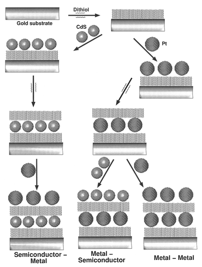 | ||
| Fig. 14 Schematic drawing depicting the layer-by-layer deposition of Pt particles onto a Au substrate, the layers being separated by dithiol molecules. Also shown is the formation of a heterostructure consisting of alternate layers of semiconductor and metal particles (from Sarathy et al.43). Reprinted with permission from J. Phys. Chem. B, 1999, 103, 399. Copyright (1990) American Chemical Society. | ||
Core-level XP spectra of superlattices of up to five layers of platinum particles (≡5 nm diameter) deposited on an Au substrate are shown in Fig. 15. We see that the intensity of the Pt(4f) feature increases with the number of depositions, accompanied by a decrease in the Au(4f) intensity as the substrate gets increasingly shadowed due to the limited escape depth of the photoelectrons. The intensities of the C(ls) and S(2p) levels of the dithiol (at 285.0 and 163.6 eV, respectively) also increase with the increasing number of depositions. A plot of the metal coverage versus the number of depositions gave a slope close to unity until the third deposition and increased thereafter suggesting that layer-by-layer deposition of nanoparticles had been accomplished.43 Brust et al.44 have reported the formation of multilayers of Au nanoparticles using dithiols. These workers have confirmed the layer-by-layer deposition of particle arrays by employing UV-vis spectroscopy and ellipsometry.
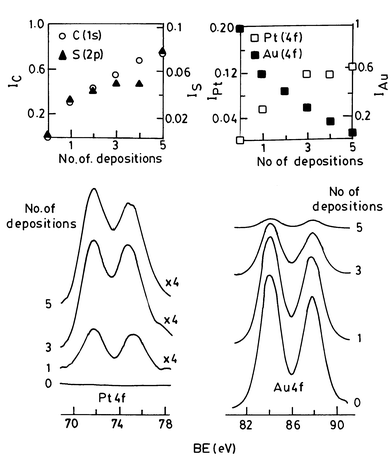 | ||
| Fig. 15 Multilayer assembly of Pt particles: XP spectra in the Pt(4f) and Au(4f) regions for the 5 nm Pt particles organised on a Au substrate. Inset shows how the Pt(4f) intensity as well as the C(ls) and S(2p) intensities (due to the thiol molecules) increase with the number of depositions while the Au(4f) from the substrate decreases (from Sarathy et al.43). Reprinted with permission from J. Phys. Chem. B, 1999, 103, 399. Copyright (1999) American Chemical Society. | ||
6 References
Acknowledgements
The authors thank the Department of Science and Technology, Government of India, for support of this research.References
- M. Faraday, Philos. Trans. R. Soc. London, 1857, 147, 145 Search PubMed.
- (a) P. P. Edwards, R. L. Johnston and C. N. R. Rao, in Metal clusters in Chemistry, Eds. P. Braunstein, G. Oro and P. R. Raithby, Wiley-VCH, 1998; Search PubMed; (b) A. I. Kirkland, P. P. Edwards, D. A. Jefferson and D. G. Duff, Annu. Rep. Prog. Chem., Sect. C, Phys. Chem., 1988, 84, 247. Search PubMed.
- W. A. de Heer, Rev. Mod. Phys., 1993, 65, 611 CrossRef CAS.
- (a) G. Schmid, Clusters and Colloids, From Theory to Applications, VCH, Weinheim, 1994; Search PubMed; (b) L. J. de Jongh, Physics and Chemistry of Metal Cluster Compounds, Kluwer, Dordrecht, 1994. Search PubMed.
- Nanoparticles and Nanostructured Films, Ed. J. H. Fendler, Wiley-VCH, Weinheim, 1998. Search PubMed.
- (a) Clusters of atoms and molecules 1, Ed., H. Haberland, Springer-Verlag, Berlin, 1994; Search PubMed; (b) C. N. R. Rao, Chemical Approaches to the Synthesis of Inorganic Materials, John Wiley, New York, 1994. Search PubMed.
- T. S. Ahmadi, L. Wang, A. Henglein and M. A. El-Sayed, Chem. Mater., 1996, 8, 428 CrossRef CAS.
- Y. Mizukoshi, K. Okitsu, Y. Maeda, T. A. Yamamoto, R. Oshima and Y. Nagata, J. Phys. Chem. B, 1997, 101, 7033 CrossRef CAS.
- R. Seshadri, G. N. Subbanna, V. Vijayakrishnan, G. U. Kulkarni, G. Ananthakrishna and C. N. R. Rao, J. Phys. Chem., 1995, 99, 5643.
- M. N. Vargaftik, I. I. Moiseev, D. I. Kochubey and K. Zamaraev, Faraday Discuss. Chem. Soc., 1991, 92, 13 Search PubMed.
- T. Teranishi, H. Hori and M. Miyake, J. Phys. Chem. B, 1997, 101, 5774 CrossRef CAS.
- (a) G. Schmidt and L. F. Chi, Adv. Mater., 1998, 10, 515 CrossRef CAS; (b) D. H. Rapoport, W. Vogel, H. Cölfen and R. Schlögl, J. Phys. Chem. B, 1997, 101, 4175 CAS.
- P.-A. Buffat, M. Flüeli, R. Spycher, P. Stadelmann and J.-P. Borel, Faraday Discuss. Chem. Soc., 1991, 92, 173 Search PubMed.
- A. I. Kirkland, D. A. Jefferson, D. G. Duff, P. P. Edwards, I. Gameson, B. F. G. Johnson and D. J. Smith, Proc. R. Soc. London A, 1993, 440, 589 Search PubMed.
- B. K. Teo, X. Shi and H. Zhang, J. Am. Chem. Soc., 1992, 114, 2743 CrossRef CAS.
- K. Asakura, Y. Yuan and Y. Iwasawa, J. Phys. IV, 1997, 7, 863 Search PubMed.
- J. Y. Yi, D. J. Oh and J. Bernhole, Chem. Phys. Lett., 1990, 174, 461 CrossRef CAS.
- (a) D. C. Johnson, R. E. Benfield, P. P. Edwards, . J. H. Nelson and M. D. Vargas, Nature, 1985, 314, 231 CrossRef CAS; (b) Y. Volokitin, J. Sinzig, L. J. de Jongh, G. Schmid, M. N. Vargaftik and I. I. Moiseev, Nature, 1996, 384, 621 CrossRef CAS.
- H. N. Aiyer, V. Vijayakrishnan, G. N. Subbanna and C. N. R. Rao, Surf. Sci., 1994, 313, 392 CrossRef CAS.
- V. Vijayakrishnan, A. Chainani, D. D. Sarma and C. N. R. Rao, J. Phys. Chem., 1992, 96, 8679 CrossRef CAS.
- R. Busani, M. Folker and O. Cheshnovsky, Phys. Rev. Lett., 1998, 81, 3836 CrossRef CAS.
- K. Rademann, O. D. Rademann, M. Schlauf, V. Even and F. Hensel, Phys. Rev. Lett., 1992, 69, 3208 CrossRef CAS.
- H. Haberland, B. von Issendorf, Y. Yufeng, J. Kolar and G. Z. Thanner, Phys. D: At. Mol. Clusters, 1993, 26, 8 Search PubMed.
- K. V. Sarathy, G. Raina, R. T. Yadav, G. U. Kulkarni and C. N. R. Rao, J. Phys. Chem. B, 1997, 101, 9876 CrossRef CAS.
- C. P. Vinod, G. U. Kulkarni and C. N. R. Rao, Chem. Phys. Lett., 1998, 289, 329 CrossRef CAS.
- M. Rosenblit and J. Jortner, J. Phys. Chem., 1994, 98, 9365 CrossRef CAS.
- R. A. Perez, A. F. Ramos and G. L. Malli, Phys. Rev. B, 1989, 39, 3005 CrossRef.
- O. D. Haberlen, S. C. Chung, M. Stener and N. Rosch, J. Chem Phys., 1997, 106, 5189 CrossRef.
- S. H. Yang, D. A. Drabold, J. B. Adams and A. Sachdev, Phys. Rev. B, 1993, 47, 1567 CrossRef CAS.
- H. N. Vasan and C. N. R. Rao, J. Mater. Chem., 1995, 5, 1755 and references therein. Search PubMed.
- K. R. Harikumar, S. Ghosh and C. N. R. Rao, J. Phys. Chem., 1997, 101, 536 CrossRef CAS.
- G. L. Hornayak, M. Kröll, R. Pugin, T. Sanitowski, G. Schmid, J.-O. Bovin, G. Karrson, H. Hofmeister and S. Hopfe, Chem. Eur. J., 1997, 3, 1951 CrossRef CAS.
- A. P. Alivisatos, K. P. Johnsson, X. Peng, T. E. Wilson, C. J. Loweth, M. P. Burchez, Jr. and P. G. Schultz, Nature, 1996, 382, 609 CrossRef CAS.
- M. Brust, M. Walker, D. Bethell, J. D. Schiffrin and R. Whyman, J. Chem. Soc., Chem. Commun., 1994, 801 RSC.
- K. V. Sarathy, G. U. Kulkarni and C. N. R. Rao, Chem. Commun., 1997, 537 RSC.
- C. J. Kiely, J. Fink, M. Brust, D. Bethell and D. J. Schiffrin, Nature, 1998, 396, 444 CrossRef CAS.
- R. L. Whetten, J. T. Khoury, M. M. Alvarez, S. Murthy, I. Vezmar, Z. Wang, P. W. Stephens, Ch. L. Clevend, W. D. Luedtke and U. Landman, Adv. Mater., 1996, 8, 428 CAS.
- S. A. Harfenist, Z. L. Wang, R. L. Whetten, I. Vezmar and M. M. Alvarez, Adv. Mater., 1997, 9, 817 CrossRef CAS.
- L. F. Chi, S. Rakers, T. Drechsler, M. Hartig, H. Fuchs and G. Schmid, Thin Solid Films, 1998, 329, 520 CrossRef.
- M. Dorogi, J. Gomez, R. G. Osifchin, R. P. Andres and R. Reifenberger, Phys. Rev. B, 1995, 52, 9071 CrossRef CAS.
- (a) J. G. A. Dubois, J. W. Gerrittsen, S. E. Shafranjuk, E. F. G. Boon, G. Schmid and H. Van Kempen, Europhys. Lett., 1996, 33, 279 Search PubMed; (b) G. Schön and U. Simon, Colloid. Polym. Sci., 1995, 273, 101 CrossRef.
- C. P. Collier, R. J. Saykally, J. J. Shiang, S. E. Henrichs and J. R. Heath, Science, 1997, 277, 1978 CrossRef CAS.
- K. V. Sarathy, P. J. Thomas, G. U. Kulkarni and C. N. R. Rao, J. Phys. Chem. B, 1999, 103, 399 CrossRef CAS.
- M. Brust, D. Bethell, C. J. Kiely and D. J. Schiffrin, Langmuir, 1998, 14, 5425 CrossRef CAS.
Footnote |
| † The terms colloid, nanoparticle and cluster, are all commonly used to describe the divided metallic state. Molecular compounds containing metal nuclei are referred to as metal cluster compounds. In this article, we have used the term nanoparticle, to represent all forms of divided metals, independent of the method of preparation. |
| This journal is © The Royal Society of Chemistry 2000 |