Issue 31, 2017

Perovskite light-emitting devices with a metal–insulator–semiconductor structure and carrier tunnelling

Abstract

Organic–inorganic hybrid perovskites have been widely recognized as highly luminescent materials for efficient light-emitting devices. Herein, we report a simple perovskite-based metal–insulator–semiconductor (MIS) device structure with green light emission. Electron tunnelling and subsequent recombination in the semiconductor–insulator interface region is confirmed as the working mechanism of the perovskite light-emitting devices.
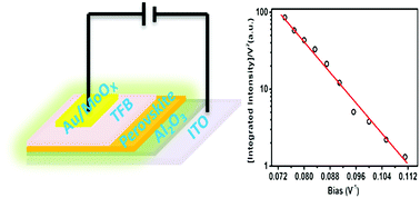
Graphical abstract: Perovskite light-emitting devices with a metal–insulator–semiconductor structure and carrier tunnelling

Supplementary files

Article information

Article type
Communication
Submitted
26 Apr 2017
Accepted
06 Jul 2017
First published
10 Jul 2017

J. Mater. Chem. C, 2017,5, 7715-7719

Perovskite light-emitting devices with a metal–insulator–semiconductor structure and carrier tunnelling

J. Li, Q. Yu, L. Gan, D. Chen, B. Lu, Z. Ye and H. He, J. Mater. Chem. C, 2017, 5, 7715 DOI: 10.1039/C7TC01809F

To request permission to reproduce material from this article, please go to the Copyright Clearance Center request page.

If you are an author contributing to an RSC publication, you do not need to request permission provided correct acknowledgement is given.

If you are the author of this article, you do not need to request permission to reproduce figures and diagrams provided correct acknowledgement is given. If you want to reproduce the whole article in a third-party publication (excluding your thesis/dissertation for which permission is not required) please go to the Copyright Clearance Center request page.

Read more about how to correctly acknowledge RSC content.

Social activity

Spotlight

Advertisements