
Light-directed growth of metal and semiconductor nanostructures
 *bc
*bc
Abstract
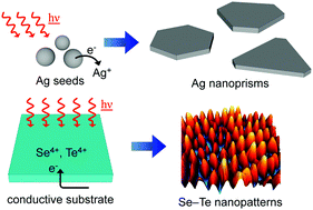
External parameters such as temperature, pressure, and concentration are typically used to control chemical transformations in molecules and materials. Many classes of inorganic materials are also responsive to external stimuli, such as electric, magnetic, and electromagnetic fields. This Review article will explore examples of how light can guide the growth of metal and semiconductor nanostructures. Plasmon excitation in metals and electronic excitation in semiconductors mediate interfacial charge-transfer reactions to alter the growth rates of these materials at the nanoscale. Light-driven growth of inorganic materials provides a route to achieve morphological control over colloidal particles and nanostructured films for potential applications in solar energy conversion, photonic computing, and holography.
- This article is part of the themed collections: Recent Review Articles and Journal of Materials Chemistry C Emerging Investigators
 Please wait while we load your content...

