
Towards an electronic grade nanoparticle-assembled silicon thin film by ballistic deposition at room temperature: the deposition method, and structural and electronic properties†

Abstract
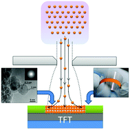
Nano-crystalline silicon attracts scientific and technological interest due to its unique tunable optical and electronic properties, which could open up the way to novel applications in fields like photovoltaics, electronics and optoelectronics. Nevertheless, the high processing temperatures and low throughputs of standard synthesis routes hinder many possible technological advances. This work presents a high-throughput technique for room-temperature synthesis of highly crystalline nanoparticle-assembled silicon thin films. Its distinctive feature is the segmentation of the deposition process in two steps: (i) nanoparticle (NP) synthesis in non-thermal plasma, and (ii) ballistic growth of NP-assembled films through a supersonic jet. Nanoparticle-assembled silicon films showing up to 50% of the bulk silicon density are synthesized with crystalline fractions and crystallite sizes in the 0–72% and 2–5.5 nm ranges, respectively. A time-of-flight technique is employed to gain insights into the transport mechanisms of charge carrier films. Photocurrent transients show dispersive behavior with mobility values up to 1.2 × 10⁻⁵ cm2 V−1 s−1, the highest thus far reported for nanoparticle-assembled silicon films directly deposited at low-temperature. A proof-of-concept field-effect transistor is fabricated by impacting NPs onto a pre-patterned substrate, demonstrating hole-current modulation. This technique holds great promises for the integration of Si-based semiconductor technology with roll-to-roll manufactured flexible electronics.
 Please wait while we load your content...

