Vacuum-process-based dry transfer of active layer with solvent additive for efficient organic photovoltaic devices†
 ‡a
O. Ok
Park
*a
and
‡a
O. Ok
Park
*a
and
Abstract
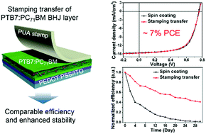
Stamping transfer process for fabricating organic electronics has recently been demonstrated to improve device performance because it allows the control of morphology, patterning, and transfer of various materials. However, it still has issues related to reproducibility because complex solvent conditions, that is, several active layers consisting of solvent additives or mixtures used for improving morphology, unfavorably affect the film transfer. To transfer uniform thin films, poly({4,8-bis[(2-ethylhexyl)oxy]benzo[1,2-b:4,5-b′]dithiophene-2,6-diyl}{3-fluoro-2-[(2-ethylhexyl)carbonyl]thieno[3,4-b]thiophenediyl}):[6,6]-phenyl-C71-butyric acid methyl ester (PTB7:PC71BM)-based organic photovoltaic cells were fabricated in this study by utilizing the optimized surface energy of the hydrophilic 2-hydroxyethyl methacrylate–polyurethane acrylate stamp. Upon application of vacuum treatment based on dry transfer, a bulk-heterojunction (BHJ) layer with the solvent additive, 1,8-diiodooctane, was completely transferred onto a poly-(3,4-ethylenedioxythiophene):poly(styrenesulfonate) (PEDOT:PSS) layer without any change in its domain distribution and composition. Consequently, BHJ devices fabricated by stamping transfer showed power conversion efficiency comparable to those of devices fabricated by spin-coating. We also observed significant improvement in long-term stability of the PTB7:PC71BM-based photovoltaic cells fabricated by stamping transfer under dry conditions.
 Please wait while we load your content...

