
Large scale ZrS2 atomically thin layers†
Abstract
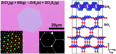
We present the scalable synthesis of large scale (up to 30 μm in lateral size), single-crystalline, atomically thin hexagonal ZrS2 nanoflakes via an optimized chemical vapor deposition (CVD) method on traditional substrates (silica, sapphire). The Vienna ab initio simulation package (VASP) was employed to calculate the adhesion energy and provided an exact theoretical account for the substrate and temperature dependent growth process of ZrS2 nanoflakes. Photodetectors based on ZrS2 nanoflakes were fabricated and displayed a remarkable photoconductivity under visible light. Field-effect transistors based on ZrS2 monolayers exhibited obvious n-type transport characteristics with relatively high mobility.
- This article is part of the themed collection: 2016 Journal of Materials Chemistry C Hot Papers
 Please wait while we load your content...

